-
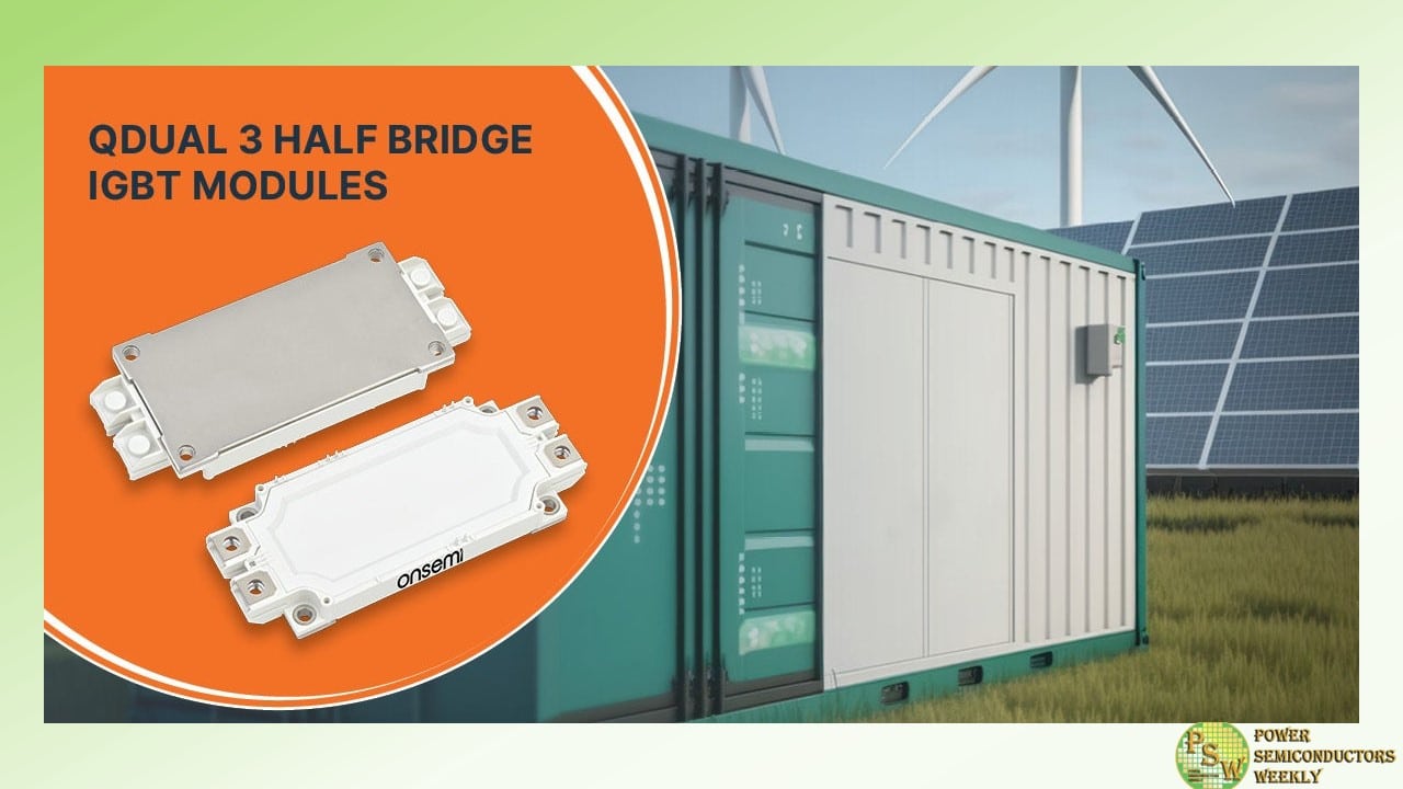
The latest onsemi 7th generation 1200V QDual3 Insulated Gate Bipolar Transistor (IGBT) power modules offer increased power density and deliver up to 10% more output power than other available competing products. Based on the latest Field Stop 7 (FS7) IGBT technology, the 800-amp (A) QDual3 module delivers industry-leading efficiency to reduce system costs and simplify designs.
In a 150KW inverter, the QDual3 module will dissipate 200 watts (W) less in losses compared to the closest competition, significantly reducing heatsink size. QDual3 is engineered to work under harsh conditions and is ideal for high-power electronics converters such as central inverters in solar farms, energy storage systems (ESS), commercial agricultural vehicles (CAVs) and industrial motor drives.
Currently, two products are available depending on the applications – NXH800H120L7QDSG and SNXH800H120L7QDSG.
Increasing renewable energy adoption amplifies the need for solutions that can manage peak demand and ensure continuous power supply. Peak shaving, the practice of reducing electricity use during peak hours, is essential for maintaining electric grid stability and reducing costs. Using the QDual3 modules, manufacturers can construct a solar inverter and ESS that output more power in the same system size, enabling more efficient energy management and storage capabilities, and allowing for a smoother integration of solar power into the grid.
The modules also mitigate the intermittency of solar energy by storing excess power in an ESS, ensuring a reliable and consistent energy flow. For large systems, the modules can be paralleled to increase the output power up to a couple of MWs and compared to traditional 600 A module solutions, the 800 A QDual3 significantly reduces the module quantity, greatly simplifying design complexity and cutting system costs.
The QDual3 IGBTs module features an 800 A half-bridge configuration that integrates the latest Gen7 trench Field Stop IGBT and diode technology using onsemi’s advanced packaging techniques to reduce switching and conduction losses.
With FS7 technology, the die size is reduced by 30%, allowing more die per module, increasing the power density to enable the maximum current capacity up to 800 A or higher. With an IGBT Vce(sat) as low as 1.75V (175°C) and low Eoff, the 800 A QDual3 module dissipates 10% lower energy losses than the next-best alternative. The modules also meet the stringent standards required of an automotive application.
“Increased electrification of commercial fleets such as trucks and busses and the need of renewable energy sources demand solutions that can generate, store and distribute power more efficiently. Transferring energy from renewable sources to the grid, storage systems and to downstream loads with the lowest power losses possible is increasingly critical,” said Sravan Vanaparthy, vice president, Industrial Power Division, Power Solutions Group, onsemi. “With its industry-standard pin-out and market-leading efficiencies, QDual3 enables power electronics designers to plug and play these modules for an immediate performance boost in their systems.”
Original – onsemi
-
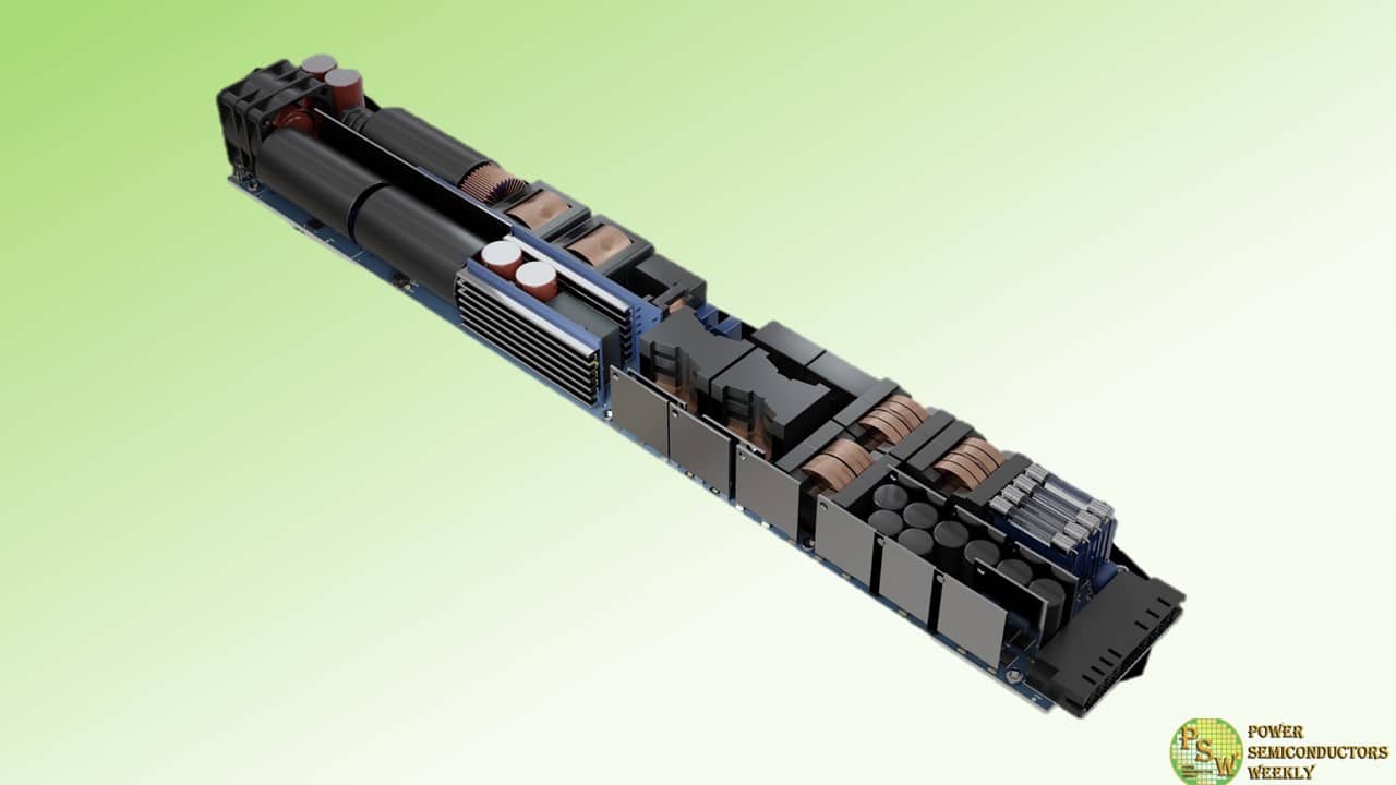
The influence of artificial intelligence (AI) is driving up the energy demand of data centers across the globe. This growing demand underscores the need for efficient and reliable energy supply for servers. Infineon Technologies AG opens a new chapter in the energy supply domain for AI systems and unveils a roadmap of energy efficient power supply units (PSU) specifically designed to address the current and future energy need of AI data centers.
By introducing unprecedented PSU performance classes, Infineon enables cloud data center and AI server operators to reduce their energy consumption for system cooling. The innovative PSUs reduce power consumption and CO 2 emissions, resulting in lower lifetime operating costs. The powerful PSUs are not only used in future data centers but can also replace existing power supply units in servers and increase efficiency.
In addition to the current PSUs with an output of 3 kW and 3.3 kW available today, the new 8 kW and 12 kW PSUs will contribute to further increasing energy efficiency in future AI data centers. With the 12 kW reference board, Infineon will offer the world’s first power supply unit that achieves this level of performance and supplies future data centers with power.
“At Infineon, we power AI. We are addressing a critical question of our era – how to efficiently meet the escalating energy demands of data centers,” says Adam White, Division President Power & Sensor Systems at Infineon. “It’s a development that was only possible by Infineon’s expertise in integrating the three semiconductor materials silicon (Si), silicon carbide (SiC), and gallium nitride (GaN) into a single module. Our PSU portfolio is therefore not only an example of Infineon’s innovative strength, which leads to first-class results in terms of performance, efficiency and reliability for data centers and the AI ecosystem. It also reinforces Infineon’s market leadership in power semiconductors.”
Infineon is responding to the requirements of data center operators for higher system efficiency and lower downtimes. The growth of server and data center applications has led to an increase in power requirements, necessitating the development of power supplies with higher power ratings from 800 W up to 5.5 kW and beyond. This increase is driven by the growing power requirements of Graphic Process Units (GPU) on which AI applications are computed.
High-level GPUs now require up to 1 kW per chip reaching 2 kW and beyond by the end of the decade. This will lead to higher overall energy demand for data centers. Depending on the scenario, data centers will account for up to seven percent of global electricity consumption by 2030; this is an order of magnitude comparable to India’s current electricity consumption.
Infineon’s new PSUs contribute to the efforts to limit the CO 2 footprint of AI data centers despite the rapidly growing energy requirements. This is made possible by a particularly high level of efficiency that minimizes power losses. Infineon’s new generation PSUs achieve an efficiency of 97.5 percent and meet the most stringent performance requirements. The new 8 kW PSU is capable of supporting AI racks with an output of up to 300 kW and more. Efficiency and power density is increased to 100 watts per in³ compared to 32 W/in³ in the available 3 kW PSU, providing further benefits for the system size and cost savings for operators.
From a technical perspective, this is made possible by the unique combination of the three semiconductor materials Si, SiC and GaN. These technologies contribute to the sustainability and reliability of AI server and data center systems. Innovative semiconductors based on wide-bandgap materials such as SiC and GaN are the key to a conscious and efficient use of energy to drive decarbonization.
The 8 kW Power Supply Unit will be available in Q1 2025. For more information about the PSU roadmap, please click here.
Infineon at the PCIM Europe 2024
PCIM Europe will take place in Nuremberg, Germany, from 11 to 13 June 2024. Infineon will present its products and solutions for decarbonization and digitalization in hall 7, booths #470 and #169. Company representatives will also be giving several presentations at the accompanying PCIM Conference and Forums, followed by discussions with the speakers. Information about Infineon’s PCIM 2024 show highlights is available at www.infineon.com/pcim.
Original – Infineon Technologies
-

Toshiba Electronic Devices & Storage Corporation held a ceremony to mark the completion of a new 300-millimeter wafer fabrication facility for power semiconductors and an office building at Kaga Toshiba Electronics Corporation in Ishikawa Prefecture, Japan, one of Toshiba’s key group companies. The completion of construction is a major milestone for Phase 1 of Toshiba’s multi-year investment program.
Toshiba will now proceed with equipment installation, toward starting mass production in the second half of fiscal year 2024. Once Phase 1 reaches full-scale operation, Toshiba’s production capacity for power semiconductors, mainly MOSFETs and IGBTs, will be 2.5 times that of fiscal 2021, when the investment plan was made. Decisions on the construction and start of operation of Phase 2 will reflect market trends.
The new manufacturing building follows and will make a major contribution to Toshiba’s Business Continuity Plan (BCP): it has a seismic isolation structure that absorbs earthquake shock and redundant power sources. Energy from renewable source and solar panels on the roof of the building (onsite PPA model) will allow the facility to meet 100% of its power requirement with renewable energy.
Product quality and production efficiency will be boosted by the use of artificial intelligence (AI). Toshiba expects to receive a grant from the Ministry of Economy, Trade and Industry of Japan to subsidize its investment in part of the manufacturing equipment.Power semiconductors play a crucial role in electricity supply and control, and are essential devices for energy efficiency in all electrical equipment. With the continuing electrification of automobiles and the automation of industrial machinery, they are expected to see continued robust demand growth. Toshiba started power semiconductor production on a new 300-millimeter wafer line in the second half of fiscal 2022 at Kaga Toshiba Electronics’ existing facility. Going forward, the company will expand production with the new fab and further contribute to carbon neutrality.
Overview of Kaga Toshiba Electronics Corporation
Location: 1-1, Iwauchi-machi, Nomi-shi, Ishikawa Prefecture, Japan
Established: December, 1984
President and Representative Director: Satoshi Aida
Employees: 1,150 (as of March 31, 2024)
Main Products: Discrete semiconductors (power semiconductors, small-signal devices and optoelectronic devices)
Web: Kaga Toshiba Electronics CorporationOriginal – Toshiba
-
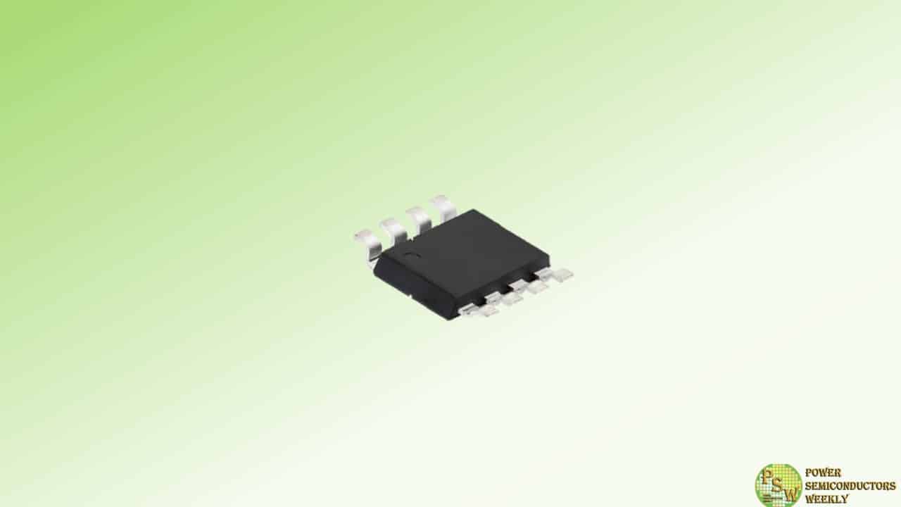
To provide higher efficiency and power density for telecom, industrial, and computing applications, Vishay Intertechnology, Inc. introduced its first fourth-generation 600 V E Series power MOSFET in the new PowerPAK® 8 x 8LR package.
Compared to previous-generation devices, the Vishay Siliconix n-channel SiHR080N60E slashes on-resistance by 27 % and resistance times gate charge, a key figure of merit (FOM) for 600 V MOSFETs used in power conversion applications, by 60 % while providing higher current in a smaller footprint than devices in the D²PAK package.
Vishay offers a broad line of MOSFET technologies that support all stages of the power conversion process, from high voltage inputs to the low voltage outputs required to power the latest high tech equipment. With the SiHR080N60E and other devices in the fourth-generation 600 V E Series family, the company is addressing the need for efficiency and power density improvements in two of the first stages of the power system architecture — power factor correction (PFC) and subsequent DC/DC converter blocks.
Typical applications will include servers, edge computing, super computers, and data storage; UPS; high intensity discharge (HID) lamps and fluorescent ballast lighting; telecom SMPS; solar inverters; welding equipment; induction heating; motor drives; and battery chargers.
Measuring 10.42 mm by 8 mm by 1.65 mm, the SiHR080N60E’s compact PowerPAK 8 x 8LR package features a 50.8 % smaller footprint than the D²PAK while offering a 66 % lower height. Due to its top-side cooling, the package delivers excellent thermal capability, with an extremely low junction to case (drain) thermal resistance of 0.25 °C/W.
This allows for 46 % higher current than the D²PAK at the same on-resistance level, enabling dramatically higher power density. In addition, the package’s gullwing leads provide excellent temperature cycle capability.
Built on Vishay’s latest energy-efficient E Series superjunction technology, the SiHR080N60E features low typical on-resistance of 0.074 Ω at 10 V and ultra low gate charge down to 42 nC. The resulting FOM is an industry-low 3.1 Ω*nC, which translates into reduced conduction and switching losses to save energy and increase efficiency in power systems > 2 kW.
For improved switching performance in hard-switched topologies such as PFC, half-bridge, and two-switch forward designs, the MOSFET released today provides low typical effective output capacitances Co(er) and Co(tr) of 79 pF and 499 pF, respectively. The package also provides a Kelvin connection for improved switching efficiency.
The device is RoHS-compliant and halogen-free, and it is designed to withstand overvoltage transients in avalanche mode with guaranteed limits through 100 % UIS testing.
Original – Vishay Intertechnology
-

Infineon Technologies AG supplies its power semiconductor devices to FOXESS, a fast-growing leader in the green energy industry and a manufacturer of inverters and energy storage systems. The two sides aim at promoting the development of green energy.
Infineon will provide FOXESS with its CoolSiC™ MOSFETs 1200 V, which will be used with EiceDRIVER™ gate drivers for industrial energy storage applications. At the same time, FOXESS’ string PV inverters will use Infineon’s IGBT7 H7 1200 V power semiconductor devices.
The global market for photovoltaic energy storage systems (PV-ES) has grown at a high speed in the last years. As competition in the PV-ES market accelerates, improving power density has become key to success, and how to improve efficiency and power density for energy storage applications has attracted much attention. Infineon’s CoolSiC MOSFET 1200 V and IGBT7 H7 1200 V series power semiconductor devices adopt the latest semiconductor technologies and design concepts that are tailored to industrial applications.
Mr. Yu Daihui, Senior Vice President and Head of Industrial & Infrastructure of Infineon Technologies Greater China said, “As an industry leader in power semiconductors, we are proud to work closely with FOXESS. We will continue to drive decarbonization by enabling higher power density and more reliable systems for PV-ES applications.”
Mr. Zhu Jingcheng, Chairman of FOXESS, said, “Thanks to the support of Infineon’s advanced components, FOXESS’ products have been significantly improved in terms of reliability and efficiency. This has been an important driving force for FOXESS’ growth. Infineon’s technical support and product quality have not only strengthened our competitiveness, but also expanded our presence in the market. We are confident about the future and look forward to further cooperation with Infineon to jointly promote the development of the industry and create greater value for our customers.”
With a high power density, Infineon’s CoolSiC MOSFETs 1200 V can reduce losses by 50 percent and provide ~2 percent additional energy without increasing the battery size, which is especially beneficial for high-performance, lightweight, and compact energy storage solutions. FOXESS’ H3PRO 15 kW-30 kW energy storage series uses Infineon’s CoolSiC MOSFETs 1200 V for all models. Thanks to Infineon’s excellent performance, the H3PRO series has achieved an efficiency of up to 98.1 percent and excellent EMC performance; with superior performance and reliability, the H3PRO series has seen rapid sales growth in the global market.
Infineon’s TRENCHSTOP IGBT7 H7 650 V / 1200 V series has lower losses and helps improve the overall efficiency and power density of inverters. In high-power inverter projects, high-current mold packaged discrete devices with current handling capability above 100 A can reduce the number of IGBTs in parallel and replace the IGBT module solution, further improving system reliability and reducing costs; in addition, the H7 series has become an industry benchmark for its high-quality performance and greater resistance to humidity.
At present, FOXESS’ main industrial and commercial model, the R Series 75-110 kW, redefines the overall design of the 100 kW model by using IGBT7 H7 series discretes, and the efficiency of the whole machine can reach up to 98.6 percent. Thanks to the low power loss and high power density of the IGBT7 H7 series in discrete packages, technical problems such as current sharing in the paralleling process can be simplified and optimized.
Every power device needs a driver, and the right driver can make the design a lot easier. Infineon offers more than 500 EiceDRIVER gate drivers with typical output currents of 0.1 A~18 A and comprehensive protection functions including fast short-circuit protection (DESAT), active Miller clamp, shoot-through protection, fault reporting, shutdown, and overcurrent protection, suitable for all power devices including CoolSiC and IGBTs.
Original – Infineon Technologies
-
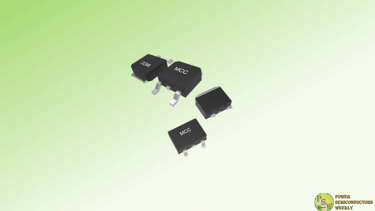
MCC Semi introduced new high-performance 40V N-channel MOSFETs. These components leverage split-gate trench (SGT) technology and full AEC-Q101 qualification in compact packages.
Both MCU2D8N04YHQ and MCB2D8N04YHQ also boast low on-resistance of only 2.8mΩ, ensuring efficient power management in a diverse range of automotive systems.
These versatile MOSFETs in high-demand DPAK and D2PAK packages ensure a seamless upgrade path with minimal changes for integration within existing designs. Adding to their unquestionable performance in harsh conditions, these components have a high operating junction temperature of up to 175°C.
Whether it’s a battery management system or electric water pump, these new MOSFETs are up for delivering the ultimate in reliability for challenging automotive applications.
Features & Benefits:
- Fully AEC-Q101 qualified
- Split-gate trench (SGT) technology
- Low RDS(on)
- High power density package
- High junction temperature up to 175℃
- Available in compact DPAK and D2PAK packages
Original – Micro Commercial Components
-
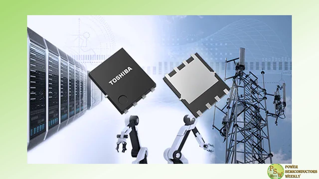
Toshiba Electronic Devices & Storage Corporation has launched two 150 V N-channel power MOSFET products that use the new generation process “U-MOSX-H series” and are suitable for switching power supplies for industrial equipment—used for such as data centers and communication base stations—and has expanded the lineup. The new products use the surface mount type SOP Advance(N) package and their drain-source On-resistance (max) is 11.1 mΩ for “TPH1100CQ5” and 14.1 mΩ for “TPH1400CQ5.”
The new products TPH1100CQ5 and TPH1400CQ5 have improved the reverse recovery characteristics that are critical in synchronous rectification applications. In the case of TPH1400CQ5, the reverse recovery charge is reduced by approximately 73 % and the reverse recovery time is approximately 45 % faster compared with Toshiba’s existing TPH1400CQH.
Used in synchronous rectification applications, TPH1400CQ5 reduces the power loss of switching power supplies and helps improve efficiency. The new products reduce the drain source spike voltage generated between the drain and source when MOSFET is switched, helping to lower EMI in switching power supplies.
Toshiba will expand its lineup of products and help to reduce power consumption for equipment.
Applications
- Switching power supplies (high efficiency AC-DC converters, high efficiency DC-DC converters, etc.)
- Motor control equipment (motor drives, etc.)
Features
- Low reverse recovery charge:
TPH1100CQ5 Qrr=32 nC (typ.) (-dIDR/dt=100 A/μs)
TPH1400CQ5 Qrr=27 nC (typ.) (-dIDR/dt=100 A/μs) - Fast reverse recovery time:
TPH1100CQ5 trr=38 ns (typ.) (-dIDR/dt=100 A/μs)
TPH1400CQ5 trr=36 ns (typ.) (-dIDR/dt=100 A/μs) - High channel temperature rating: Tch (max)=175 °C
Original – Toshiba
-

The aviation industry’s requirements for the latest, most efficient and lowest-emission aircraft is propelled by an overarching goal towards sustainability and decarbonization. To satisfy these goals, aviation power systems developers are transitioning to electric actuation systems as the trend towards More Electric Aircraft (MEA) continues to grow.
To provide the aviation industry with a comprehensive electric actuation solution, Microchip Technology announced a new integrated actuation power solution that combines companion gate driver boards with the expansive Hybrid Power Drive (HPD) modules in silicon carbide or silicon technology with a power range of 5 kVA to 20 kVA.
The new integrated actuation power solution maintains the same footprint regardless of the power output. The companion gate driver boards are designed to be integrated with Microchip’s HPD modules to provide an all-in-one motor drive solution for the electrification of systems such as flight controls, braking and landing gear. Microchip’s power solutions are designed to scale based on the requirements of the end application, from smaller actuation systems for drones to high-power actuation systems for Electric Vertical Take-Off and Landing (eVTOL) aircraft, MEA and all-electric aircraft.
“We developed the companion gate driver boards to be used with our existing HPD modules to bring to market a plug-and-play power solution for MEA,” said Leon Gross, vice president of Microchip’s discrete product group. “With this solution, customers no longer need to design and develop their own drive circuitry, which can reduce design time, resources and cost.”
These high-reliability devices are tested to conditions outlined in DO-160, “Environmental Conditions and Test Procedures for Airborne Equipment.” There are multiple protection features including shoot-through detection, short circuit protection, desaturation protection, Under Voltage Lock Out (UVLO) and active miller clamping.
The gate driver boards are designed to be driven with external PWM signals based on Low Voltage Differential Signaling (LVDS) compliant with TIA/EIA-644 for low Electromagnetic Interference (EMI) and good noise immunity. The gate driver board provides differential outputs for telemetry signals like DC bus current, phase current and solenoid current by taking feedback from shunts present in the HPD module and DC bus voltage. It also provides direct output of two PT1000 temperature sensors available in the HPD power module.
The companion gate driver boards are low-weight, low-profile and compact solutions to optimize size and power efficiency of actuation systems. The gate drivers are designed to operate throughout the temperature range of −55°C to +110°C, which is critical for aviation applications that are often exposed to harsh environments.
The isolated companion gate driver boards only require a single 15V DC input for the control and drive circuit; additional voltages needed can be generated on the card. This significantly reduces the number of system components and simplifies system cabling.
Microchip provides comprehensive solutions for MEA by integrating power products with FPGAs, microcontrollers, security, memory and timing. Microchip’s solutions are designed to help customers speed up their development, reduce costs and get to market faster.
Original – Microchip Technology
-
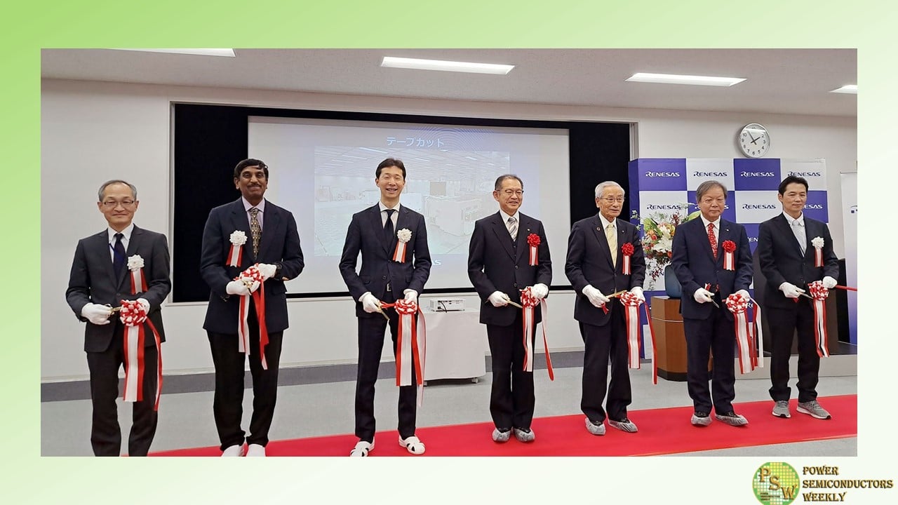
Renesas Electronics Corporation announced that it has started operations at its Kofu Factory, located in Kai City, Yamanashi Prefecture, Japan. Renesas aims to boost its production capacity of power semiconductors in anticipation of the growing demand in electric vehicles (EVs). To celebrate this milestone, Renesas held an opening ceremony on April 11 with local government officials and partner companies in attendance.
The Kofu Factory previously operated both 150mm and 200mm wafer fabrication lines under Renesas Semiconductor Manufacturing Co., Ltd, a wholly owned subsidiary of Renesas, but ceased operations in October 2014. Renesas made the decision to re-open the factory in May 2022 as a 300-mm wafer fab to support the growing demand for power semiconductors, which is propelled by the industry-wide goal to realize a decarbonized society.
Renesas conducted a 90-billion-yen worth investment in 2022 and has now started operations. The factory will start mass production of IGBTs and other products in 2025, doubling Renesas’ current production capacity for power semiconductors.
“We are proud to announce a remarkable achievement of the Kofu Factory. After its closure in 2014, the Kofu Factory has gone through a transformation and emerged as a dedicated 300-mm wafer fab for power semiconductors, exactly a decade later,” said Hidetoshi Shibata, President and CEO of Renesas.
“We extend our heartfelt thanks to the local governments of Yamanashi Prefecture, Kai City and Showa Town as well as the plant construction companies, equipment vendors, outsourcing and other partner companies. The power semiconductors produced at the Kofu Factory will help maximize the effective use of electricity, which will be in significant demand as EVs and AI continue to proliferate and advance.”
Outline of the Kofu Factory:
- Official Name: Kofu Factory, Renesas Semiconductor Manufacturing Co., Ltd.
- Address: 4617 Nishiyahata, Kai City, Yamanashi Prefecture, Japan
- Date Opened: April 1, 2024
- Size of Clean Room: up to 18,000 square meters
- Products to be Manufactured: IGBTs, Power MOSFETs and other power products
Original – Renesas Electronics
-
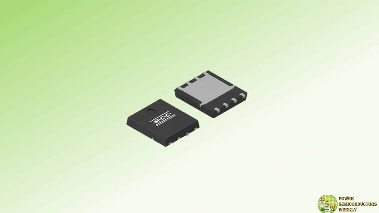
Micro Commercial Components introduced the latest auto-grade N-channel power MOSFETs with up to 2.5mΩ on-resistance: MCACL220N06YHE3, MCACL2D5N06YL, MCACL280N04YHE3, and MCACL330N04YHE3.
Optimized for high current output, these powerful components boast RDS(on) as low as 0.8mΩ in a sleek, engineer-friendly DFN5060 package. You can enhance power management and ramp up efficiency with minimal losses and the confidence that come along with AEC-Q101 qualification and the MCC name.
With high power density, MCC’s new 40V and 60V MOSFETs are designed to handle harsh conditions and operating junction temps up to 175℃ with ease, making them ideal for diverse automotive and industrial applications — from battery management systems and electric power steering to lighting controls, water pumps, and solar power systems.
Features & Benefits:
- AEC-Q101 qualified for reliability
- Advanced split-gate trench (SGT) technology
- Excellent thermal performance & efficiency
- Low RDS(on) minimizes power losses
- High power density packagey
- High junction temperature up to 175℃
- Compact DFN5060 package saves space and material costs
Original – Micro Commercial Components


