Abstract
This paper presents a high-speed level shifter with about 500 V/ns power supply slew immunity. In this designed structure, a narrow pulse-controlled current source is adapted to accelerate the voltage conversion and reduce the power consumption. A Fast-Slewing Circuit speeds up the operation of the level shifter based on the current comparison principle.
Edge detection technology is used to filter the generated voltage noise and achieve high dV/dt immunity. The proposed level shifter simulated with the 0.18 μm BCD (bipolar-CMOS-DMOS) process shows fast responses with a typical delay of 1.49 ns and 500 V/ns dV/dt immunity in the 200 V high-voltage application, which only occupies a 0.022 mm2 active area with the 0.18 μm BCD process.
1. Introduction
In recent years, the continuous growing markets in 5G communications, wireless transmission, fast charging industries, etc., create a huge demand for advancing today’s high-voltage (HV) power converters for cost and energy savings. Silicon-based power semiconductor devices have reached their physical limits due to their restrictions on device size and their physical characteristics. Although the switching losses in power devices can be reduced by applying technologies like soft switching, the large gate parasitic capacitance of silicon-based devices limits the optimization of energy loss, which affects the performance of power converters under high-input-voltage and high-frequency conditions [1].
Wide-bandgap (WBG) semiconductor materials, such as silicon carbide (SiC) and gallium nitride (GaN), have been demonstrated to offer excellent features compared to silicon. For instance, wide-bandgap (WBG) semiconductor materials allow smaller, faster, more reliable power electronic components than their silicon-based counterparts [2]. The wide-bandgap power devices exhibit greater thermal conductivity and electric field strengths, and as a result, SiC and GaN power devices have lower on-resistance to reduce conduction losses [3].
Therefore, the wide-bandgap GaN and SiC devices have gradually replaced the original silicon-based power semiconductor devices for their excellent performance advantages, producing a technological revolution in the fields of information communication, electric vehicles, and consumer electronics [4,5,6,7].
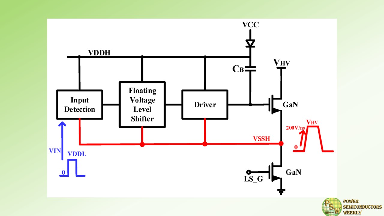
Usually, SiC and GaN power devices are used in half-bridge drivers as power switches. Level shifters are commonly employed as a transmission bridge between different voltage domains to shift the potential of the control logic from the low-voltage domain to the high-voltage domain or from the high-voltage domain to the low-voltage domain [8]. The high-voltage domain mainly includes level shift, high-side drive, and bootstrap circuits.
Unlike the supply voltage of the low-voltage domain (usually a fixed voltage below 5 V), the high-voltage domain is powered by floating power rails (VDDH and VSSH). When the high-side power transistor is turned on, the low-voltage VSSH of the floating power rail is approximately equal to the input voltage VHV of the half-bridge driver, and the high-voltage VDDH of the floating power rail is equal to VSSH + VCC.
To turn on and off the high-side power transistor, the high-side driver needs to run on a floating power rail. The logic control signal is from the low-voltage domain and must be transformed to a high-voltage domain logic signal. As shown in Figure 1, the low-voltage control signal is sent to the level shifter after going via the Input Detection module, which activates or deactivates the high-side power transistor.
Therefore, as a bridge connecting the high-voltage domain and the low-voltage domain, the level shifter is one of the most critical circuits in the half-bridge driver. However, the GaN and SiC MOSFET can generate larger dV/dt and di/dt noise in the fast switching. For GaN MOSFET, the dV/dt could be up to above 200 V/ns [9]. This fast slewing is particularly problematic on the high side of the half-bridge driver, as shown in Figure 1.
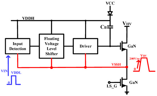
Figure 1. The block diagram of the GaN high-voltage half-bridge driver.
Figure 2 shows the reliability issues with traditional GaN drivers. When the high-side power transistor is activated, the voltage of VSSH will be quickly raised to VHV, and the rising speed is >200 V/ns. This dVSSH/dt change is coupled to the level shifter through a bootstrap capacitor. Since the level shifter can perform voltage conversion between the low-voltage domain and the high-voltage domain, MH1 and MH2 are high-voltage transistors, whose parasitic capacitance is large.
The parasitic capacitance will generate a charging or discharging current when dV/dt happens, which will interfere with the level shifter’s normal operation and cause errors in the driver’s logic voltage of the high-voltage domain [10,11,12]. In Figure 2, it can be seen that under the action of the bootstrap capacitor CBOOT, VDDH changes with VSSH, and dVDDH/dt is approximately equal to dVSSH/dt. However, since the input MOS device MH1 of the level shifter is a high-voltage transistor, there is a large parasitic capacitance Cpar at node A.
The rapid change of the VDDH acts on Cpar to generate a large current, which pulls down the voltage of node A. When the noise amplitude (=R × Cpar × dVSSH/dt) generated at node A is larger than (VBOOT − VT), the recovery circuit of the subsequent stage may transmit the noise signal by mistake, where VBOOT is equal to VDDH − VSSH. Therefore, the dV/dt immunity capability of the driver is limited by the parasitic capacitance of the HV transistor of the level shifter.
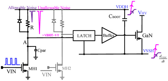
Figure 2. Reliability problem of the traditional level shifter.
Existing high-voltage level shifters have employed a number of design techniques to improve dV/dt immunity [13,14,15]. In [13], the author proposed a level shifter based on high-bandwidth current and latch structure; the delay is 370 ps, but the dV/dt slew immunity is only 30 V/ns. Yang et al. adopted a new technique to enhance the slew rate of level shifters, achieving a novel level shifter with 120 V/ns immunity and 20 ns propagation delay [14].
The level shifter (LS) proposed in [15] is designed with a current mirror/latch structure, and a common-mode noise canceller is also applied to enhance the dV/dt immunity. This level shifter achieves 200 V/ns noise immunity and sub-nanosecond delay in the SOI process, but this good performance is limited by the process. As the supply voltage increases, level shifters made with traditional processes suffer more from dV/dt noise. Then the ensuing problem is that the level shifter needs to consume more energy to enhance the dV/dt immunity of the circuit. As a result, several conventional structures designed to enhance the dV/dt noise immunity of the level shifters become inappropriate as the power supply voltage rises.
This paper presents a high-speed and high dV/dt immunity floating-voltage level shifter in the 0.18 μm BCD process. The proposed design can achieve a small propagation delay and an ultra-high dV/dt noise shielding function.
The rest of this paper is organized as follows: In Section 2, two conventional level shifter designs are reviewed. In Section 3, a novel enhanced level shifter is proposed, and its propagation delay and dV/dt immunity are analyzed in detail. Section 4 and Section 5, respectively, display the simulation results and conclusion.
2. Previous Level Shifter
A conventional level shifter is shown in Figure 3 [16]. The MOS transistors M1–M4 are high-voltage transistors. LDNMOS (laterally diffused N type metal oxide semiconductor) transistors M1 and M2 connect their gates to VDDL to protect and clamp the low-voltage (LV) transistors ML1 and ML2. In addition, the circuit connects the gates of the LDPMOS (laterally diffused P type metal oxide semiconductor) transistors M3 and M4 to VSSH to protect the low-voltage transistors ML5 and ML6 from being damaged by breakdown.
This circuit can convert the low-voltage power rail signal from GND-VDDL to the high-voltage floating power rail signal VSSH-VDDH. However, LDNMOS and LDPMOS transistors increase the parasitic capacitance and cause large propagation delays. More seriously, this structure suffers from mismatch delay and low dV/dt noise immunity. This level shifter has inconsistent low-to-high and high-to-low conduction delays due to the current asymmetry between the rising and falling edges of the output node.
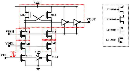
Figure 3. Traditional level shifter based on high-voltage PMOS clamping.
Figure 4 shows another type of conventional level shifter [17]. This topology clamps the voltage at nodes N1 and N2 to VDDH − VGS by using the diode-connected low-voltage PMOS transistors M1 and M4, where VGS is the gate-source voltage of the PMOS transistors. When the input signal VIN switches from low to high, the high-voltage tube LDNMOS1 is turned on; then the potential of the N1 point is pulled down, and the potential of the N2 point rises.
However, the potential at point N1 decreases more slowly than the potential at point N2 rises due to the current asymmetry. In the same way, when the VIN switches from high to low, the high-voltage tube LDNMOS2 is turned on; then the potential of the N2 point is pulled down, and the potential of the N1 point rises. The falling speed of the potential at point N2 is slower than the rising speed at point N1. For the structure in Figure 4, only a pair of high-voltage transistors, LDNMOS1 and LDNMOS2, are used, which has a lower parasitic capacitance than the structure in Figure 3. However, this level shifter faces the same difficulties as the structure shown in Figure 3, namely, that there is a severe mismatch delay and low dV/dt noise immunity.
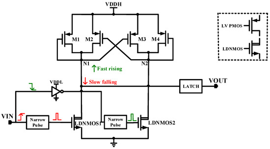
Figure 4. Traditional level shifter based on diode-connected PMOS clamping.
3. Proposed Enhanced Level Shifter
As shown Figure 5, this paper presents a high-speed and high dV/dt immunity level shifter which consists of three parts: the Power Supply Rail Conversion Circuit, the Fast-Slewing Circuit (FSC), and the dV/dt Noise Shielding Circuit. The Power Supply Rail Conversion Circuit converts the signal from the low-voltage domain to the high-voltage domain. The Fast-Slewing Circuit speeds up the level shifter’s signal conversion. And then the dV/dt Noise Shielding Circuit can shield the dV/dt noise to make the output of the level shifter remain constant.
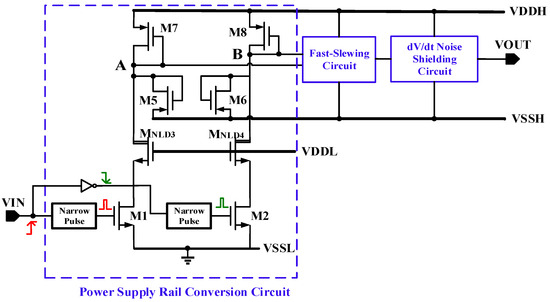
Figure 5. Top structure and strategy of the proposed level shifter.
In Figure 5, the input transistors M1 and M2 are low-voltage MOS devices. The diode-connected transistors M7 and M8 are used to clamp the voltages of node A and node B. The gate of the high-voltage transistors MNLD3 and MNLD4 are connected to the low-voltage rail power supply VDDL to bear high voltage, preventing the breakdown of the low-voltage transistors M1 and M2. The M5 and M6 transistors are used in the form of diodes, with their sources connected to the floating power supply ground VSSH to ensure that the voltages of node A and node B can be higher than VSSH − VTH (VTH is the threshold voltage of the MOSFET).
This prevents the drain-source voltage of the M7 and M8 devices from exceeding the safe voltage range. A narrow pulse generation circuit is adopted to generate the instantaneous driving signal and speed up the operation of the level shifter [18]. Additionally, the Fast-Slewing Circuit that was added to the circuit can speed up the voltage conversion rate of the level shifter even more, eliminating the issue of various mismatch delays.
The problem of dV/dt immunity is the most important concern of the level shifter, which can be analyzed from the two situations of positive swing and negative swing of the power supply. As shown in Figure 6, when the VIN is high, the normal states of VA − VSSH and VB − VSSH are low voltage and high voltage, respectively. When VSSH and VDDH quickly transition from high voltage to low voltage, both VA − VSSH and VB − VSSH rise to high voltage.
When VSSH and VDDH transition from low voltage to high voltage, both VA − VSSH and VB − VSSH can drop to low voltage. Therefore, the dV/dt Noise Shielding Circuit is meant to maintain the level shifter’s output in order to avoid the succeeding stage circuit from receiving the erroneous signal output of the level shifter.
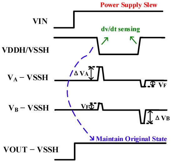
Figure 6. Noise shielding feature for dV/dt when the VIN is high.
3.1. Strategy for the Enhanced Level Shifter
The level shifter proposed in this article is shown in Figure 7. The signal conversion of the level shifter can be sped up by using the Fast-Slewing Circuit and the double-pulse generation circuit. The double-pulse generation circuit can generate a voltage pulse on the rising and falling edges of an input signal, consisting of a NAND gate, a capacitor, and several inverters. In the proposed level shifter, the input of this double-pulse generation circuit is the signal of the VIN, and the output of the circuit is used to control the on and off of M1 and M2.
Therefore, whenever there is a conversion of high voltage to low voltage or low voltage to high voltage, a large current will appear in the voltage conversion branch, improving the voltage conversion speed. At the same time, the transistors M1 and M2 are turned off during the voltage holding stage, so that the level shifter has very low static power consumption.
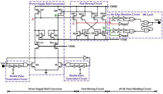
Figure 7. Schematic of the proposed level shifter circuit.
The Fast-Slewing Circuit is a current mirror that makes use of the principle of current comparison to achieve rapid voltage conversion speed [19]. As can be seen in Figure 7, when the VIN signal transitions from low voltage to high voltage, the voltage of node A can drop rapidly with the help of the huge pull-down capability of the transistor M1, while the asymmetric current of the circuit causes the voltage of node B to rise slowly.
Therefore, the proposed level shifter adopts the Fast-Slewing Circuit to improve the response speed. The voltages at nodes A and B are mirrored to nodes D and C through a current mirror, respectively, after passing through the Fast-Slewing Circuit, preventing the circuit from various mismatch delays. Then, the rising edge of node C or D can be captured by the edge detection circuit and locked by the SR latch, which finally changes the output of the level shifter and keeps it constant until the VIN changes.
3.2. The Propagation Delay of the Proposed Level Shifter
The proposed level shifter’s operation for switching from low to high is shown in Figure 8a. Before the VIN becomes high, VA is equal to VDDH, and VB is equal to VSSH. The signal transmission process of the level shifter is as follows:
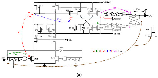
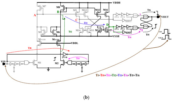
Figure 8. The suggested level shifter’s switching operation: (a) low-to-high switching operation; (b) high-to-low switching operation.(1)
When the VIN changes from low voltage to high voltage, the generation circuit, which consists of a NAND gate, a capacitor, and several inverters, generates a voltage pulse on the rising edges of the VIN signal. The delay in this process is called Tr0, which is determined by the delay of the NAND gate.(2)
When the voltage pulse generates, the input transistor M1 is turned on, and the voltage VA at node A begins to drop rapidly. The delay in this process is called Tr1. The strong pull-down capability of M1 will briefly provide a large current to the branch where node A is located to increase the response speed of node A.(3)
The current M7 is mirrored by the M9. Due to the small current of M10, the current of M9 is much greater than that of M10, so the potential at node C is rapidly raised to VDDH. The Tr2 is the transmission delay from node A to node C, which is determined by the delay of the current comparator.(4)
The edge detection circuit can identify the rising edge signal of node C. When VC becomes high, a short pulse signal is generated at node S under the action of the delay chain composed of INV1-INV3 and NAND1. Tr3 is the delay of the edge detection circuit.(5)
The generation of a short pulse signal VS triggers the flipping voltage of NAND4. At this point, the VOUT transitions from low to high and remains at VDDH until a short pulse occurs at node R. The delay between VS and VOUT is described by Tr4, which is the delay of NAND4.
The current of M7 can also be mirrored to M15 through M13 and M14. Due to the small current of M16, the voltage at node D is quickly pulled down. Although the descent speed of VD is slower than the ascent speed of VA, the drop of VD is not detected by the edge detection circuit and is just prepared for the next reset. Therefore, when the input signal VIN changes from low to high, the speed at which the voltage at node D changes has no effect on the circuit.
As shown in Figure 8b, when the input voltage of the level shifter transitions from high to low, the propagation delay Td_f of the signal consists ofTf0, Tf1, Tf2, Tf3, Tf4, Tf5, and Tf6. Due to the good symmetry of the proposed level shifter, Tr0 is equal to Tf1, Tr1 is equal to Tf2, Tr2 is equal to Tf3, Tr3 is equal to Tf4, and Tr4 is equal to Tf5. Therefore, it can be seen that Td_f has two more delay items, Tf0 and Tf6, than Td_r, which are the delays of the two NAND gates. Therefore, Td_r is smaller than Td_f.
3.3. The dV/dt Immunity of the Proposed Level Shifter
The edge generation circuit of the proposed level shifter has two functions. One is that the edge generation circuit can output a pulse signal at the rising edge and falling edge of the input signal; on the other hand, the edge generation circuit generates a large current during the narrow pulse signal to help the signal transfer quickly, and reduces the overall power consumption of the circuit by turning off the input transistors M1 and M2 during the VIN signal hold.
The transient operation of the proposed level shifter is demonstrated with low-to-high and high-to-low operations. When the VIN shifts from low to high, M1 is activated and M2 is turned off. The voltage at node A starts declining, the dropping edge of node A is sampled, and the rise of node C is accelerated by the current comparison circuit. The rising edge of node C is delayed by the delay circuit composed of the inverters INV1–INV3, and then the delayed signal is input to NAND1 together with the signal of node C. Next, a low-voltage pulse signal S is generated, and then the voltage of the VOUT changes from low to high.
When the input signal VIN changes from high to low, M2 is turned on, and M1 is turned off. The voltage at node B begins to drop, and then the falling edge of node B is sampled, which speeds up the rising speed of node D. The rising edge of node D can be delayed by the inverters INV4–INV6 and this delayed waveform is input into NAND2 with node D. At this time, a low-level pulse is generated in R to make the VOUT change from high to low. Figure 9 shows the waveform of the level shifter during the VIN transient changes.
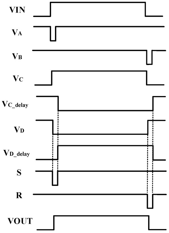
Figure 9. The waveform of the level shifter during VIN transient changes.
The proposed level shifter can shield dV/dt noise by using the dV/dt Noise Shielding Circuit, which consists of INV1–INV6 and NAND1, NAND2. The voltages at nodes C and D will rise or fall synchronously when dV/dt noise is generated due to rapid changes in the VSSH and VDDH. If the dV/dt noise is high, voltage changes at nodes C and D may trigger the logic gates of the edge detection circuit. Positive dV/dt noise will cause undershoot voltage at nodes C and D, and negative dV/dt noise will cause overshoot at nodes C and D.
However, these generated voltage noises will be filtered after passing through the edge detection circuit, so that no error signals will be generated at the S and R terminals, and the state of the RS latch will not be changed. Therefore, the proposed level shifter can shield the dV/dt noise from disturbing the output VOUT, so that the VOUT can remain constant.
4. Simulation Results
The proposed level shifter is simulated at the 0.18 μm BCD process using the Cadence Virtuoso tool. Figure 10 shows the simulated propagation performance of the proposed level shifter with 205 V VDDH and 200 V VSSH under the typical process corner. All power rails are supplied with fixed voltage sources during simulation (VDDH − VSSH = 5 V, VDDL = 5 V). The VIN is operated under 5 V supply voltage, and the low voltage of the VOUT is 200 V and the high voltage is 205 V.
It can be seen from Figure 10 that when the rising edge of the VIN is generated, the voltage at node A drops and triggers the low-voltage pulse signal of the S terminal of the RS flip-flop, and then the VOUT starts to flip from low to high. The voltage at node B decreases when the falling edge of the VIN arrives; then the R terminal of the RS flip-flop generates a low-voltage pulse signal, and the VOUT starts to change from high to low. The simulation results show that the propagation delay of the rising edge is about 1.23 ns, and the propagation delay of the falling edge is about 1.75 ns.
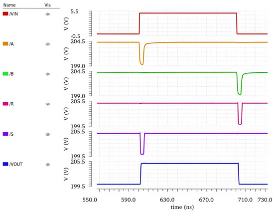
Figure 10. Propagation delay of the proposed level shifter.
Figure 11a,b show the rising and falling delays of the proposed level shifter under three process corners, ss (Worst Case), tt (Typical Case), and ff (Best Case), at temperatures −55 °C and 150 °C. The simulation results show that the minimum rising delay is 479 ps and the maximum is 2.64 ns; the minimum falling delay is 842.1 ps and the maximum is 3.4 ns.
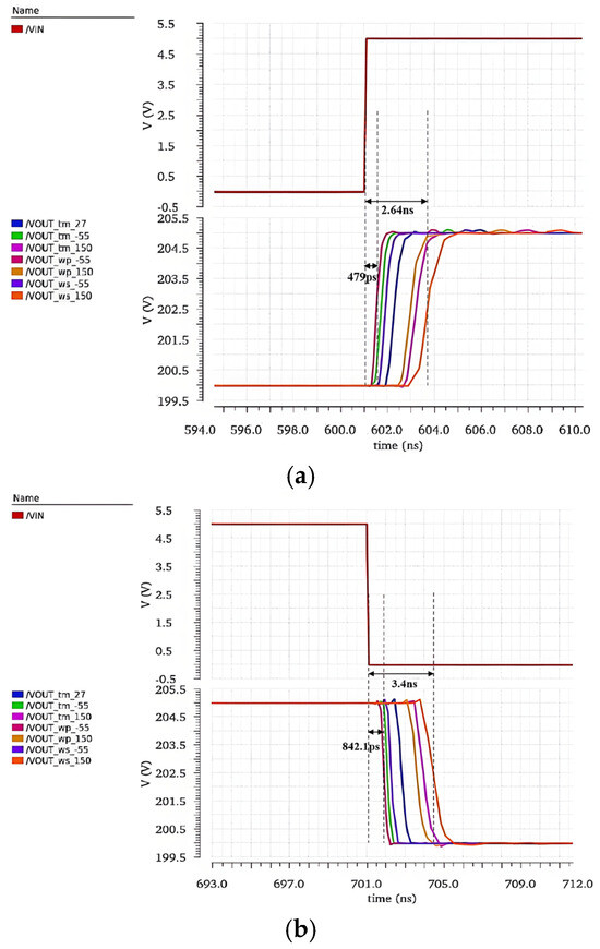
Figure 11. Simulation results of the proposed level shifter’s delay: (a) rising delay; (b) falling delay.
Figure 12 simulates the dV/dt noise shielding function of the proposed level shifter at ±500 V/ns dV/dt noise. The simulation results show that when dV/dt noise is generated, the voltages VS and VR have no erroneous logic signals during the period when the input signal VIN is high, the output signal VOUT is not disturbed by dV/dt noise, and the state remains unchanged.
Therefore, this can demonstrate that the level shifter proposed in this paper can achieve ±500 V/ns dV/dt immunity, which is also suitable for other supply voltages and processes. Figure 13 shows the layout of the proposed level shifter. The chip area is only 127 μm × 178 μm at the 0.18 μm BCD process.
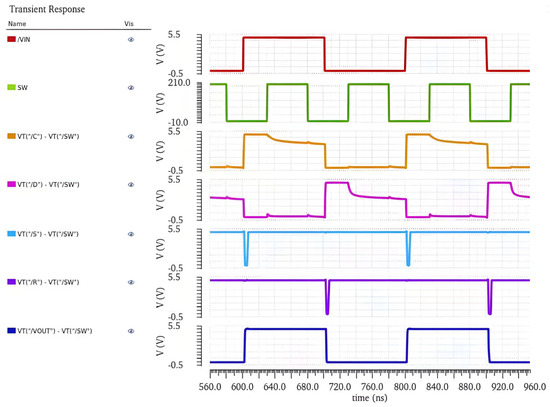
Figure 12. Simulation results of the dV/dt noise shielding function of the proposed level shifter.
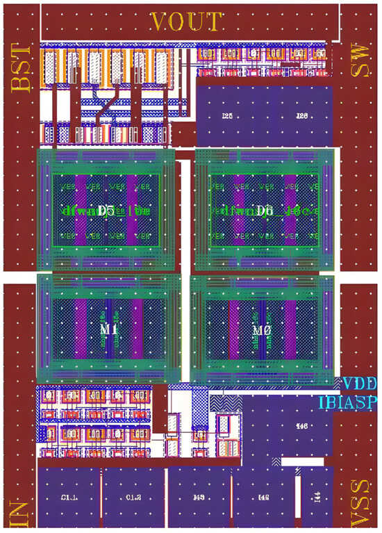
Figure 13. The layout of the proposed level shifter.
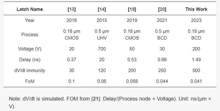
Table 1 shows the performance comparison between the proposed level shifter and previous reported level shifters. FOM is used to evaluate the performance of the level shifter by combining delay, supply voltage, and process node. It can be seen from Table 1 that the high-voltage level shifter proposed in this paper has the highest dV/dt immunity and the smallest FOM. Therefore, the proposed level shifter can still achieve sufficient response speed and high reliability under a 200 V power supply.
Table 1. Comparison with previous work.
5. Conclusions
This paper presents a high-voltage level shifter for a GaN half-bridge driver that offers high-speed operation and high dV/dt immunity. A narrow pulse-controlled current source and the Fast-Slewing Circuit speed up the transmission of the level shifter and reduce the power consumption. Edge detection technology is utilized to filter the generated voltage noise and then achieve the ultra-high dV/dt immunity of the level shifter without using complex auxiliary circuits.
In the 0.18 μm BCD process, the proposed level shifter can achieve a propagation delay of 1.49 ns and a 500 V/ns dV/dt immunity under a 200 V power supply, which only occupies a 0.022 mm2 active area. The FOM is very small, which is only 0.041. The suggested level shifter can be utilized in multi-MHz converters because of its low propagation delay and its ability to provide 500 V/ns of slewing immunity, making it suitable for drivers of wide-bandgap power device applications.
Authors
Min Guo, Lixin Wang, Shixin Wang, Yuan Zhao and Bowang Li
Original – MDPI