Abstract
The design and optimization of power converters is a key factor in the growth and development of the power electronics field. However, the process of designing a power converter is not straightforward, and engineers often rely on experience and intuition, sometimes requiring time-consuming computer simulations. This paper presents a tool for the basic design of grid-connected AC–DC converters. The design tool takes specifications and operating conditions for two-level and three-level NPC converter topologies and derives a draft design.
The tool calculates the input filter’s electrical parameters, the converter’s losses, the temperature rise of the power semiconductor devices, and the ripple current and voltage of the DC-link capacitor. In order to validate the proposed design tool, four AC–DC converters using SiC MOSFETs were designed. Based on the design results, simulation models and prototypes were fabricated to verify the performance and confirm that the proposed design tool can be used in the basic design process of converters.
1. Introduction
As the field of power electronics continues to evolve, the design and optimization of power converters is a key factor in the efficient conversion and utilization of energy. Power converters in various forms, such as AC–DC converters and DC–DC converters, play an important role in power management, motor control, and more in a variety of applications such as renewable energy systems, electric vehicles, industrial automation, and home appliances. The ability to design these power converters precisely and efficiently is crucial for meeting the energy efficiency, reliability, and sustainability requirements of the ever-evolving energy industry [1].
However, the process of designing a power converter is far from simple. There are complex tradeoffs between design features such as the power circuit structure, control scheme, and switching frequency and performance metrics such as efficiency, voltage ripple, and current ripple. Engineers designing power converters often rely on experience and intuition, and in some cases, complex computer simulations, to achieve optimal results. Even experienced professionals can find it difficult to design with new converter topologies, control schemes, etc., and it can take a lot of trial and error to learn how to do it, especially for newcomers to the field [2,3].
To solve this problem, studies have been conducted on procedures and methods for designing various types of power converters. References [4,5,6] present step-by-step procedures for designing power converters with specific converter topologies or introduce tools that can assist in the design. These works are mainly aimed at finding the optimal design point to achieve the targeted performance metrics when the basic design of the power converter is already completed. However, this approach can be difficult for someone not already familiar with the design of this type of converter.
Recently, methods using artificial intelligence (AI) have been studied to automate and reduce the reliance on experts in the converter and controller design phase [7,8,9,10]. These methods are well suited for use in the optimization design phase for specific target systems. However, AI-based design methods have the disadvantage of requiring simulations under various specifications and operating conditions to collect data, and the selection of appropriate training methods and the training process may require a considerable amount of resources.
Alternatively, basic power converter design tools are available, often provided by power semiconductor manufacturers [11,12]. However, the applicable converter topologies are limited, and device selection is also limited by the only components manufactured by the design tool vendor.
To address these issues, this paper introduces a general converter design tool for power converter design. The research project “Development of High Efficiency Power Converter based on Multidisciplinary Design and Optimization Platform”, funded by the Korea Institute of Energy Technology and Planning (KETEP), aims to build and operate an open web-based design tool for various power conversion systems based on wide-band-gap (WBG) semiconductors [13].
The design tool proposed in this paper is intended to be used in the basic design phase and is intended to quickly check feasibility or to quickly see how a particular performance varies as a function of parameter variation. The intention is to save the user of the design tool the effort of calculating formulas or building simulation models by hand. The tool is a synthesis of state-of-the-art research and practical engineering expertise and aims to simplify and popularize the process of power converter design and optimization. It provides engineers and researchers with an intuitive and user-friendly interface, allowing them to efficiently explore different design outcomes with a large number of degrees of freedom. It enables them to optimize the design parameters and ultimately deliver a high-performance solution for their specific needs.
These design tools can help accelerate the development of power conversion systems, foster innovation, and enable the rapid adoption of new technologies. Furthermore, they have the potential to popularize power conversion design knowledge. The popularization of this knowledge can play an important role in the development of new technologies and paving the way for a more sustainable and efficient future in power electronics.
This paper introduces a general power conversion design tool for grid-connected AC–DC converters as part of the general converter design tool. The design tool developed requires the ability to allow the user to select different types of components available on the market during the design process. For this purpose, it is difficult to use data that must be obtained through complex experiments, and it is possible to use only the level of information disclosed in the datasheets provided by the manufacturers of the devices. The proposed design tool also aims to have simple formulas and design procedures so that they can be used in a lightweight web-based design tool.
The proposed design tool primarily tackles the complexity inherent in power converter design. While traditional design methods heavily rely on complex computer simulations, the proposed tool simplifies this aspect, allowing for faster, more rapid, and more accessible design iterations. By making the design process more accessible and less dependent on deep expertise, the proposed tool helps to popularize power converter design knowledge, which is crucial for promoting innovation in the field.
In the next section, the procedure for the basic system design of an AC–DC converter is presented, and the formulas used in each design step are derived. Based on the proposed design procedure, the design of converters of various specifications was carried out, and simulation models and prototypes were produced based on the designed parameters to verify the results of the design tool.
2. Design Procedures
This paper presents a design tool for grid-connected three-phase AC–DC converters using SiC MOSFETs among various types of power conversion devices. The design tool aims to facilitate the drafting of designs by engineers with little experience in converter design. Figure 1 shows the design procedure. Viewing the converter as an electrical circuit composed of lumped elements, the basic specifications, such as the input and output voltages, capacity, and converter topology, are first selected. Limits are set on the efficiency, voltage and current ripple, and temperature rise of the semiconductors, and the switching devices are selected.
The input parameters include operating conditions such as the switching frequency and power factor, along with the previously selected items. Based on the input parameters, the tool calculates the ripple of the input current, the voltage and current ripple of the DC-link, derives the electrical parameters of the input filter and the DC-link capacitor, and calculates the converter loss and temperature rise to check whether the limit conditions are met.
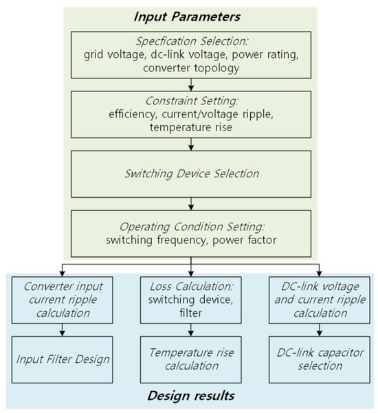
Figure 1. Grid-connected AC–DC converter design procedure.
However, this tool is intended for use in the basic design phase of a converter. In order for the web-based design tool to display design results quickly, the design procedure is based on simple formulas, and a certain amount of error is allowed. To develop a real product-level converter, more detailed design steps are required.
The component-level design of passive devices, such as inductors used in converters, component placement and mechanical structure design for power density optimization, and the electromagnetic field analysis and heat distribution analysis, which require finite element analysis, are not covered in this paper. The process and formulas used in the design tool are as follows.
2.1. Input Filter Design Procedure
In a grid-connected AC–DC converter, the purpose of the input filter is to reduce current harmonics at the input side caused by voltage harmonics generated by PWM switching. As an input filter circuit, a simple inductor or an LCL filter consisting of two inductors and one capacitor is commonly used. The design tool in this paper exploits an LCL filter that has high harmonic rejection performance per unit inductance.
Figure 2 shows the structure of the AC–DC converter and the LCL filter discussed in this paper. Lc and Lg represent the converter-side and grid-side inductors, respectively, and the filter capacitor, Cf, is connected in series with the damping resistor, Rd. The power stack is represented by a three-phase, two-level (2L) voltage-type inverter structure, which assumes the use of a three-phase, two-level or three-level (3L)-NPC converter in this paper.
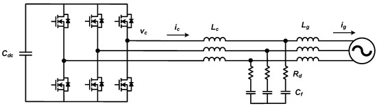
Figure 2. Grid-connected AC–DC converter structure with LCL filter.
Ignoring the effect of damping resistors in the converter structure of Figure 2, the relationship between voltage harmonics and current harmonics can be expressed as follows.

where ig is the grid-side current and vc is the output voltage at the converter side. The order-specific harmonics of the output voltage due to the switching of the converter can be calculated analytically [14]. With the limits of the target harmonic currents for each order, the input filter can be designed using the relationship in (1).
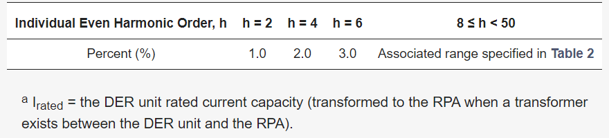
Table 1, Table 2 and Table 3 show the current harmonic limits by order of the current harmonic regulations IEEE-519 [15] and IEEE-1547 [16], which are widely used in designing grid-connected AC–DC converters. Studies on designing input filters have used the relationship in (1) to select input filter parameters that ensure that the voltage harmonics caused by the PWM of the converter do not exceed the current harmonic limits of each regulation [17,18].
Table 1. Current harmonic limits according to the IEEE 519 standard [15].
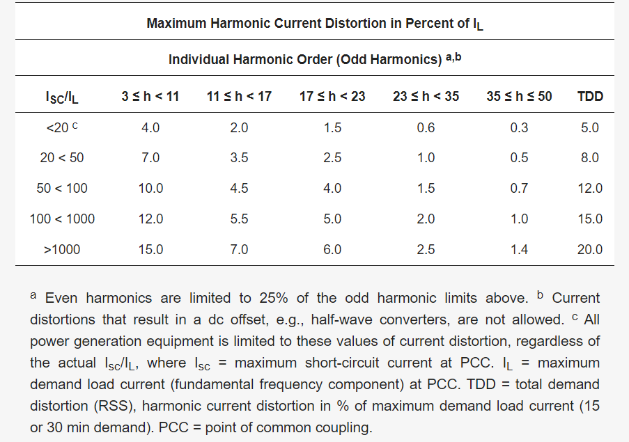
Table 2. Odd harmonic current distortion limit in percent of rated current (Irated) a according to IEEE 1547 [16].
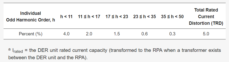
Table 3. Even harmonic current distortion limit in percent of rated current (Irated) a according to IEEE 1547 [16].
However, this approach may not be appropriate for converters using SiC MOSFETs. As shown by the relationship in (1), harmonics in the grid current are caused by harmonics in the output voltage due to the PWM operation of the converter. The output voltage harmonics can be roughly divided into two classes according to their order: higher-order harmonics around multiples of the PWM switching frequency and lower-order harmonics corresponding to multiples of the fundamental wave, such as the 5th, 7th, 11th, etc.
The higher-order voltage harmonics can be calculated analytically according to the PWM method by obtaining the magnitude of the harmonic voltage of each order, and filter parameters can be designed accordingly to limit the harmonic current of that order to a target value or less.
However, higher-order harmonics often account for a smaller proportion of the total current harmonic component generated by a grid-tied converter than lower-order harmonics. This is because higher-order harmonics have higher frequencies and are more easily attenuated by the input filters.
This is especially true for converters using SiC MOSFETs, which often have switching frequencies of tens of kHz or more. Furthermore, popular grid input current harmonic regulations, IEEE 519 [15] and IEEE 1547 [16], limit the harmonic frequency to no more than the 50th order of the fundamental wave. For converters using SiC MOSFETs, most have switching frequencies above 20 kHz, so the higher-order harmonics associated with the switching frequency are well beyond the 50th order when referenced to the typical grid frequency of 60 Hz, which is outside the harmonic regulation criteria.
When using input filters to satisfy grid current harmonics regulations, it is then necessary to design them with low-order current harmonics in mind, but it is difficult to accurately calculate the magnitude of the voltage harmonics that cause low-order current harmonics.
Low-order output voltage harmonics are due to the non-ideal output characteristics of the converter, such as dead time and a voltage drop across switching elements, and are difficult to obtain analytically. In addition, for converters using SiC MOSFETs with fast switching frequencies, harmonic current controllers can be used to significantly suppress low-order harmonics [17]. In practice, harmonic current controllers are often used, which can lead to overly large filter designs if their effects are not considered. However, the harmonic control performance of the controller is also difficult to accurately estimate at the filter design stage.
In this paper, an input filter design method based on limiting the maximum value of the ripple of the converter-side current below a certain value is used, rather than limiting the grid current harmonics below a certain value according to the regulations of [15,16], etc. The design procedure of the input filter is shown in Figure 3, and the detailed design process is as follows.
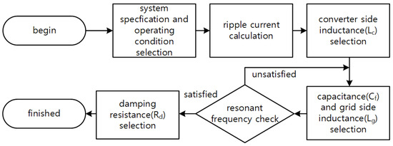
Figure 3. Inpul filter design procedure.
- Select system specifications and operating conditions. Select the grid voltage, grid frequency, converter type (2L or 3L-NPC), switching frequency, DC-link voltage, and rated current.
- Calculate ripple current and select converter side inductance. Set the converter-side ripple current limit. Select the limit value of the peak-to-peak amplitude of the current ripple relative to the rated current and calculate the converter-side inductor value that satisfies the ripple current according to the operating conditions. The peak-to-peak amplitude of the ripple current generated by the converter is determined by the operating conditions, and the instantaneous phase angle and can be expressed as (2) [18].

where Vdc is the DC-link voltage, Ts is the switching period, and r(m,θ) is a function of the voltage modulation index (m) and the output voltage phase angle (θ). The magnitude of the instantaneous current ripple depends on the phase angle, but the proposed method calculates the magnitude of the current ripple based on the output voltage at a phase angle of 90°.
In general, the power factor of a grid-connected converter is close to unity, so the output voltage and current are almost in-phase, and the magnitude of the current flowing in the converter is maximized around 90 degrees. Therefore, when considering the maximum current flowing through the converter due to current ripple, it is appropriate to base the design on the value when the phase angle is 90°. The converter-side inductance (Lc) value that satisfies the magnitude of the ripple current can be selected by using (2).
- Select capacitance and grid-side inductance. The larger the capacitor of the LCL filter, the better it can absorb the converter’s ripple current and reduce the harmonics of the grid-side current. However, the capacitor in the input filter introduces reactive power at the grid side and changes the grid side power factor. Typically, the reactive power flowing into the capacitor is limited to 2–5% of the apparent power in the design of the input filter [19]. The proposed design tool takes the reactive power value of the capacitor as input and selects the capacitor divisor of the corresponding filter. The formula for selecting the capacitance value is shown in (3).

where S is the apparent power of the converter, ω is the frequency of the grid, Vph is the phase voltage of the grid, and R is the ratio of the reactive power to the apparent power. In studies dealing with LCL filter design, the values of the grid-side inductance and the converter-side inductance are often chosen to be equal. This is because, when the resonant frequency of the LCL filter is first determined, equalizing the two inductance values results in the smallest magnitude of the total inductance [20], i.e., the harmonics of the grid current can be reduced the most with the same inductance value.
However, in this paper, the filter is designed based on the ripple current on the converter side, not the current harmonics delivered to the grid. In the case of converters using SiC MOSFETs, the low-order harmonics that contribute most to the grid current harmonics can be significantly suppressed by current controllers, so the proposed method focuses more on the converter-side inductor in the total inductance used in the input filter. In this paper, the grid-side inductance is selected as one-third of the converter-side inductance.
- Check the resonant frequency of the input filter. The resonant frequency (fres) of the input filter should be less than one-half of the sampling frequency (fs) according to the Nyquist sampling theory, and it should be higher than the bandwidth (fb) of the current controller to avoid affecting the current control behavior [21].

Finally, check whether the parameters of the input filter selected satisfies (4), and if not, adjust the capacitance value so that the resonant frequency satisfy the limitation of (4).
- Select damping resistor. The LCL filter theoretically has zero impedance at its resonant frequency. The damping resistor is used to provide impedance at this time to suppress the oscillation of the current at the resonant frequency. For this purpose, the value of the damping resistor is designed to be similar to the impedance of the capacitor connected in series at the resonant frequency [22], and in this paper, it is selected as one-third of the impedance of the capacitor at the resonant frequency.

2.2. Calculating Losses and Temperature Rise
The losses of the converter covered in this paper are composed of the losses of the power semiconductor and the losses of the input filter. The losses are calculated based on the given converter specifications and operating conditions, and the junction temperature is estimated using the thermal resistance information of the heat sink where the power semiconductor is installed.
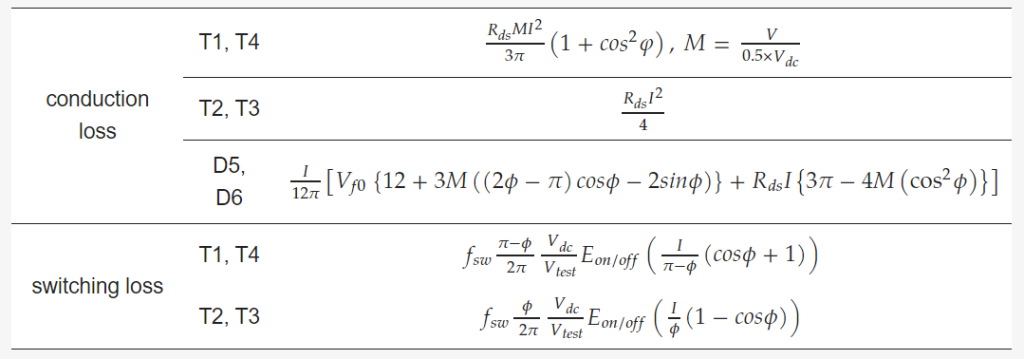
The losses of the power semiconductor can be divided into conduction losses and switching losses. The conduction losses of SiC MOSFETs and diodes are calculated using the Rds, Rd, and Vf0 information in the datasheet, as shown in (6) and (7), respectively, and the switching losses of SiC MOSFETs are calculated using the datasheet loss data, as expressed in (8).

where Rds is the equivalent resistance when the SiC MOSFET is turned on and Rd and Vfo are the equivalent resistance and threshold voltage when the diode is turned on, respectively. Irms is the rms value of the current flowing in each power semiconductor device, fsw is the switching frequency, s(θ) is duration when the current is flowing in that semiconductor device, Iavg is the average current in the current flowing section, Vdc is the DC-link voltage, Vtest is the test voltage indicated in the switching loss data in the datasheet, and Eon/off is the loss function extracted from the on and off switching loss data in the datasheet. The gate resistance is inputted by the user and reflected in the determination of Rds and Eon/off.
Equation (8) uses the average current in the conducting section to calculate the switching losses under the assumption that the current flowing in the device at the time of switching is proportional to the switching losses. In practice, the two are not exactly proportional. In general, for SiC MOSFETs, there is a slight exponential increase in switching losses as the current flowing through the device at the time of switching increases.
As a result, the switching losses calculated from the average current tend to be smaller than the actual switching losses at higher load currents, leading to calculation errors. However, since the design tool presented in this paper is intended to be used in the basic design phase for feasibility checks, this level of error can be justified. Overcurrent and overvoltage due to parasitic components like stray inductance also affect the switching loss [23]. However, the parasitic component cannot be anticipated during the basic design phase, so it is not reflected.
Figure 4 shows the leg structure of the two-level and three-level converters covered in this design tool, and the output voltage command and output current of the converter are shown in (9) and (10).

where V and I represent the magnitude of the output voltage command and output current, respectively, ω is the frequency of the grid, and φ is the load angle. In order to calculate the loss of each power semiconductor device, the operating region can be divided into four according to sign of output voltage command and output current.
Figure 5 shows the four operating areas with the state of the output voltage command and current. Table 4 summarizes the current-carrying devices and devices where switching losses occur in each operating area for 2L and 3L-NPC converters. Using Figure 5 and Table 4, it is possible to calculate the rms value of the current flowing through each power semiconductor element, the average current in the section where the current flows, and substitute the values into (6)–(8) to calculate the loss for each element in each converter, as shown in Table 5 and Table 6.
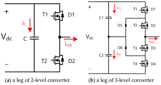
Figure 4. Leg configuration of AC–DC converters.
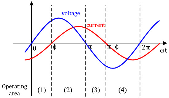
Figure 5. Operating area classification.
Table 4. Switch operation according to operating area.
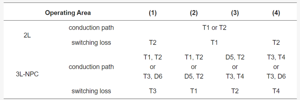
Table 5. Power semiconductor loss for 2L converter.
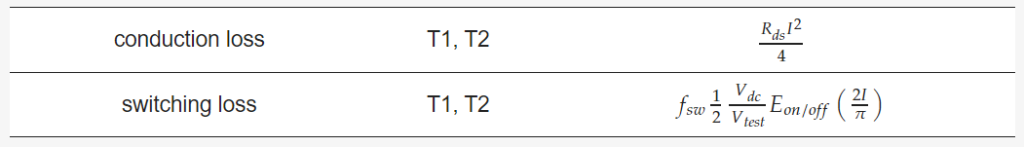
Table 6. Power semiconductor loss for 3L-NPC converter.
The calculated losses of the power semiconductor are used to calculate the junction temperature rise of the power semiconductor. Figure 6 shows the heat transfer circuit model used to calculate the temperature rise in this paper. The losses generated by the power semiconductor are denoted as Ploss, and the thermal resistance from the junction of the power semiconductor to the case, the thermal resistance from the case to the heat sink, and the thermal resistance from the heat sink to the atmosphere are denoted as Rth,jc, Rth,ch, and Rth,ha, respectively. Tjunction, Tcase, Theatsink, and Tamb represent the junction, case, heatsink, and ambient temperatures, respectively.
The heat capacity of each part is not considered, but only steady-state losses and thermal resistance are considered to calculate the junction temperature. Rth,jc and Rth,ch use the datasheet values of the semiconductor device, and Rth,ha of the heat sink can be entered to be used to calculate the temperature rise, as shown in (11).

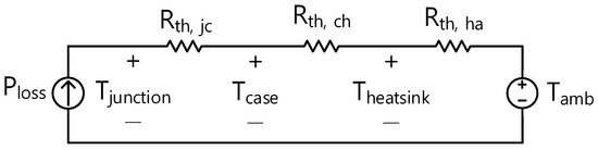
Figure 6. Heat transfer circuit.
More precisely, thermal resistance could be expressed as a function of temperature [24]. However, as shown in [24], for accurate modeling, the parameters should be obtained through testing for each component used in the converter, which is difficult to achieve with a basic design tool for various different types of components. The thermal resistance in this paper uses nominal values from the datasheet.
Most of the losses in the input filter come from the inductor. The loss of the inductor is determined by the design conditions, such as the core and winding used in the inductor, and the operating conditions, such as the magnitude and frequency of the voltage and current applied to the inductor. The conduction losses of an inductor are calculated using the resistance calculated from the cross-sectional area and length of the inductor windings, and the effective value of the current flowing in the inductor and the iron losses are calculated using the Steinmetz equation shown in (12) [25].

The coefficients required for the Steinmetz equation were obtained from the core’s datasheet information and added together by calculating the losses at the fundamental and switching frequencies. The flux density (B) was calculated using the magnitude of the fundamental wave current and the maximum ripple current magnitude, calculated using (2).
2.3. DC-Link Voltage, Current Ripple Calculations
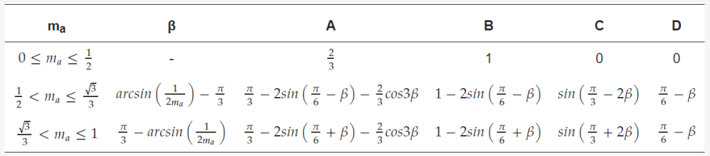
The design tool in this paper derives the minimum DC-link capacitance values required during the converter design process. With the given system specifications and operating conditions, the DC-link capacitor currents of the 2L and 3L-NPC converters (iC of the 2L converter and iC1/iC2 of the 3L-NPC converter in Figure 4) can be calculated analytically, as shown in (13) and (14), respectively [26,27]. Table 7 shows the detailed formulas for the parameters used in (14).

Table 7. Expressions of A, B, C, and D in (14).
Taking the limit value of the voltage ripple as the input, the minimum value of the DC-link capacitor that satisfies the limit value can be selected as follows [26].

The tool selects the minimum value of the DC-link capacitor through equation (15) and derives the minimum value of the ripple current rating of the capacitor through (13) or (14).
3. Design Examples
Many cases of grid-connected AC–DC converters were designed using the converter design tool introduced in this paper. Table 8 shows the specifications and operating conditions of the design cases. All of them are 10 kVA-class grid-connected AC–DC converters and use 2L and 3L-NPC NPC converter topologies.
The grid to which they are connected is assumed to be typical three-phase 380 V 60 Hz converters. The current ripple ratio indicates the magnitude of the ripple current relative to the rated current. Cases 1 and 2 and cases 3 and 4 have identical specifications except for the current ripple specification, resulting in designs with different input filters.
Table 8. Specification and operating conditions for design cases.

Table 9 shows the minimum values of the input filter and DC-link capacitance derived from the design tool. In (2), the current ripple magnitude of the 2L converter is generally larger compared to the 3L-NPC converter, resulting in a larger inductance despite the higher current ripple limit of the 2L converter.
The minimum value of the DC-link capacitor resulting from the design is less than 10 μF, so in practice, the converter design should be based on selecting a capacitor that meets the current ripple rating. In such a design, the capacitance of the actual capacitor used is considerably larger than the minimum capacitance derived from the design tool, so that the voltage ripple caused by the current ripple is negligible.
Table 9. Input filter design results.

4. Simulation and Experimental Results
Based on the results of the design tool introduced in this paper, simulation models and prototypes were produced and compared with the design values. For the four cases of circuits in Table 8 and Table 9, simulation models were created using PSIM (version 9.0), and prototypes were fabricated and compared with the experimental results.
Figure 7 is a photo of the experimental set of one of the fabricated prototypes. The current ripple of the fabricated converter was measured using an oscilloscope, and the efficiency was measured using a power meter. The temperature rise was measured by attaching an NTC to the heatsink where the power semiconductor was installed.
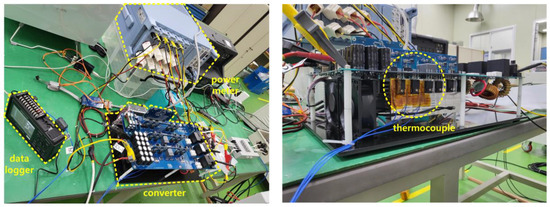
Figure 7. Experimental setup with prototype converter.
Figure 8 shows the waveforms of the fabricated simulation and the prototype. They represent the input line voltage, converter current, and grid current, respectively. It can be seen that the experimental waveforms have similar characteristics to the simulation results and behave appropriately.
Both the experimental and simulation results show that the ripple of the converter-side current varies with the circuit topology and the parameters of the input filters, but the harmonics of the grid-side current are not significantly different in all four cases. It can be seen that the low-order harmonics, which have a significant impact on the grid-side current quality, are sufficiently suppressed by the current controller.
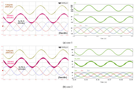
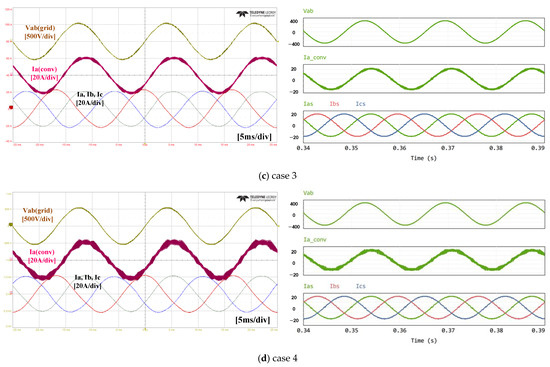
Figure 8. Experimental and simulation waveforms.
Table 10 shows the design values and experimental results of the current ripple, temperature rise, and THD of the grid current. For these metrics, only results at a rated load are compared, as their maximum values are considered during the design phase. The current ripple is similar to the design value for the 2L converter, while the 3L-NPC converter shows more deviation from the design value. In the 3L-NPC converter, the parasitic inductance along the switching path is larger due to the increase in the number of power semiconductor devices and the complexity of the busbar structure of the PCB, and the voltage spikes generated during switching have the effect of making the current ripple larger.
The THD of the grid-side current is not considered in the design tool introduced in this paper, but the measured current THD is shown to confirm that the input filter, considering only the converter-side ripple current, can keep the current THD low enough if a sufficiently good PR controller is used under a fast switching frequency. The temperature rise was calculated by measuring the temperature of the heatsink near where the power semiconductor is attached, as shown in Figure 7. In the model in Figure 6, the power semiconductor losses were calculated as Ploss and compared to Theatsink’s calculations and measurements.
The heatsink model was calculated with a simple concentrated integer thermal resistance, and the temperature of three heatsinks near the power semiconductor was measured and averaged. For the 2L converter, the temperature rise difference between the design and experimental results is smaller, but for the 3L-NPC converter, the deviation is relatively larger. In the case of the 2L converter, the number of semiconductor devices and the size of the heat sink are smaller, so the heat transfer structure is simpler and more in line with the simple model in Figure 6, but in the case of the 3L-NPC converter, the placement structure of the power semiconductor devices and the heatsink is relatively more complex, which is estimated to cause a slight deviation from the model.
Table 10. Current ripple, THD, and temperature rise of design value and experimental results.
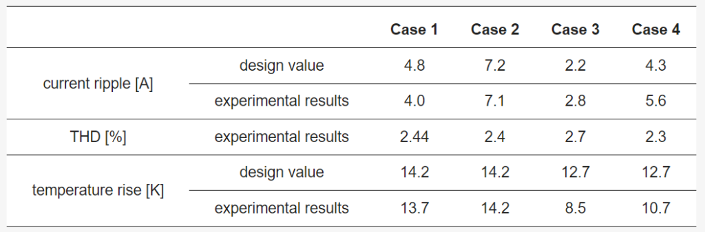
Figure 9 shows the calculated efficiency of the design tool and the measured efficiency from the experiment. The losses in the power semiconductor and the losses in the input filter were used to calculate the efficiency. Overall, the deviation between the measured and calculated efficiency at low loads is large, and the error decreases as the load factor increases.
At light loads, the iron losses in the input filter account for a large portion of the total losses, and it is assumed that the iron losses calculated through (12) are different from the actual losses incurred, leading to the error. The flux density is used as an input variable to calculate the iron loss in Equation (12). In the proposed design tool, the flux density is derived based on the maximum value of the current ripple calculated in (2).
However, in practice, the magnitude of the current ripple varies with the phase angle [28]. In the phase section where the current ripple is reduced, the flux density is also reduced, resulting in smaller iron losses. As a result, the calculated value of iron loss is larger than the actual value. Further improvements in flux density variation according to phase angle may be needed to increase the precision of the iron loss calculation. However, as a tool used in the basic design phase of a converter, it can be considered to have a reasonable calculation error. It is also appropriate that the calculation error is reduced under heavy loads, as efficiency at higher load factors is generally considered more important.
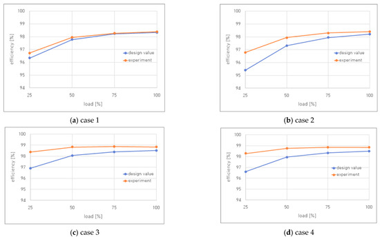
Figure 9. Efficiencies vs. loads of design value and experimental results.
5. Conclusions
This paper presents a design tool for designing three-phase grid-connected AC–DC converters. The basic design procedures for drafting the system design of a 2L or 3L-NPC converter were introduced, and the theory and formulas used in each design procedure were presented. The introduced design tools view the converter as an electrical circuit composed of lumped elements and set basic specifications, such as the input and output voltages, capacitance, converter topology, and limit conditions, such as the efficiency, voltage and current ripple, and temperature rise, and select switching elements.
Based on the input parameters, the ripple of the input current, DC-link voltage, and current ripple are calculated to derive the electrical parameters of the input filter and DC-link capacitor, and the converter losses and temperature rise are calculated to verify that the limit conditions are met.
The input filter uses the LCL filter structure, which is widely used in grid-connected converters. To limit the converter-side ripple current, the converter-side inductor value is determined first, and the grid-side inductor value is set accordingly. The capacitor value is determined according to the user-entered reactive power magnitude limit, and the damping resistor value is set to make the impedance of the input filter at the resonant frequency large enough.
Then, to calculate the efficiency, the converter losses are calculated. There are two main types of losses discussed in this paper: power semiconductor losses and input filter losses. The power semiconductor losses are calculated using the device’s datasheet information. The rms and average current flowing in each device are calculated and applied to the datasheet information of the power semiconductor device to calculate the conduction and switching losses.
The temperature rise is calculated using the thermal resistance information of the semiconductor device, the heatsink, and the previously calculated losses of the semiconductor device. The losses of the input filter are calculated by calculating the copper and iron losses of the inductor.
The current ripple in the DC stage is calculated analytically using the given system specifications and operating conditions. The calculated current ripple is used to find the minimum value of the DC-link capacitor that satisfies the voltage ripple given as a limit.
Using the introduced design tool, the converter design for various conditions is carried out and validated through a simulation and experiment. For four 10kVA-class converters, the design tool was used to derive the parameters of the input filter and the minimum value of the DC-link capacitor, and simulation models and prototypes were built based on the derived values and compared with the results of the design tool.
The experimental results showed that the temperature rise and current ripple magnitude were similar to the results of the design tool. The measured efficiency showed some deviation from the calculated value in the light-load region, but overall, the trend of efficiency change with load factor was similar in the design value and the experimental result, and the difference in the absolute values was small, showing that it is suitable as a basic design tool.
Authors
Original – MDPI