
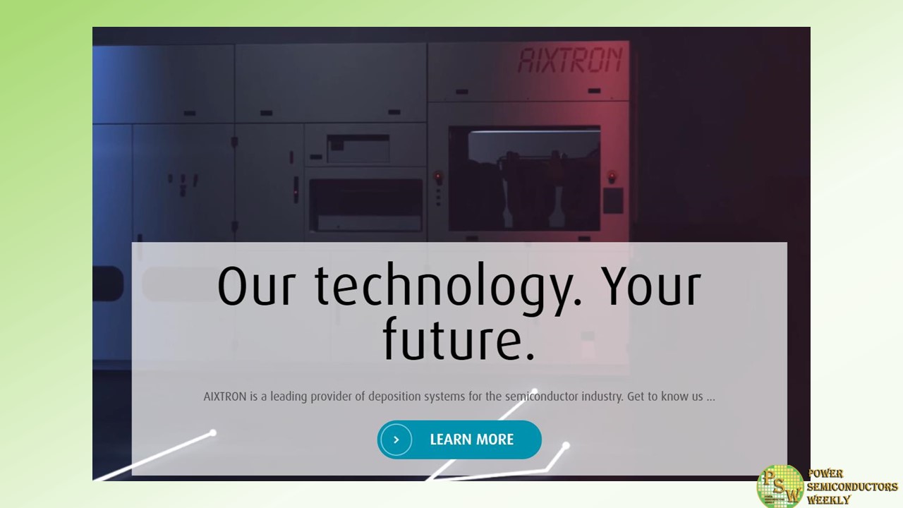
AIXTRON SE plans to invest up to 100 million euros at its Herzogenrath site. A new innovation center is to be built, which will provide the manufacturer of deposition equipment to the semiconductor industry with enhanced capacities for research and development. AIXTRON received approval for the new project from the company’s Supervisory Board.
The new innovation center will provide 1000m2 of cleanroom space and will be built on the company’s premises in Herzogenrath, Germany. The new building will create further capacities for the next product generations which are already in preparation, as well as for further product developments beyond that.
“With our products, we address the megatrends of digitalization, electromobility and energy efficiency and are experiencing a strong and steadily growing demand. Technical innovations and product developments that precisely address the needs of our customers are the key to our success. And our dynamic environment offers us further growth opportunities,” says Dr. Felix Grawert, CEO of AIXTRON SE. “We are therefore very pleased that the Supervisory Board has approved this project which will enable us to create the foundation for further product developments and for future growth.”
The importance of product development in the dynamic semiconductor industry is demonstrated by the success of AIXTRON’s new “G10” system generations. In the first year after market introduction, AIXTRON expects to generate more than 40 percent of its annual revenues with this new product generation. Right after its official launch, the new tool for the silicon carbide material system (G10-SiC) has already generated a high order intake. And it is expected to continue to drive further growth all throughout 2023 and beyond.
Also, the new AIXTRON solution for the gallium-arsenide/indium-phosphite material system (G10-AsP) which was launched at the beginning of 2023 already enjoys a strong demand. For the first time, it enables the high-volume production of Micro LEDs and photonic components such as lasers on wafers with a diameter of up to 200mm. Later in the year, the new G10 system for gallium nitride (GaN) will also be launched. The material systems SiC and GaN have the potential to fully cover the complete range of power electronics, from electromobility to renewable energy technologies to fast data transmission. With their outstanding material properties, they will ensure a significant reduction in global CO2 emissions in these areas and help electromobility achieve a breakthrough.
Original – AIXTRON


