-

Toshiba Electronic Devices & Storage Corporation and Toshiba Corporation (Toshiba Group) have developed technology that mitigates the parasitic oscillation that occurs during switching operations by power modules with silicon carbide (SiC) MOSFETs connected in parallel, even with a 60% smaller gate resistance than is typical. The technology reduces power loss in power modules, mitigates oscillation, and realizes highly reliable switching operations.
The drive for carbon neutrality is stimulating demand for technologies that improve energy efficiency in many areas, including renewables, railways, and industrial equipment. In these sectors, the application of power modules built around SiC MOSFETs is seen as a solution that supports high-speed switching at high voltages and large currents—which is particularly important for the miniaturization of power converters, where higher switching frequencies result in higher rates of switching losses against power consumption.
Connecting multiple chips in parallel in power modules can form oscillation circuits, the result of wiring inductance between the chips and their parasitic capacitance. It can reduce module reliability if not countered, which is usually done by increasing gate resistance. However, this approach slows switching speed, resulting in a trade-off with switching losses. For power modules with SiC MOSFETs to perform high-speed switching, another approach is needed.
Toshiba Group used an equivalent circuit model of the power module (Figure 1) to determine the theoretical condition that triggers parasitic oscillation, and developed a wiring layout less likely to cause it. This was done by analyzing simulations of parasitic oscillation occurs when Lg/Ls, the ratio of gate-to-gate inductance Lg and source-to-source inductance Ls of parallel chips, is below a certain value (Figure 2). As increasing Lg/Ls is an effective means of mitigating parasitic oscillation, Toshiba Group fabricated prototype modules with different Lg/Ls and measured switching. This confirmed that increasing Lg/Ls mitigated oscillation, even with a 60% smaller gate resistance than that required by the alternative approach of increasing gate resistance (Figure 3).
Applying this approach to oscillation mitigation in power modules now under development has realized a power module less likely to cause parasitic oscillation, even with minimal gate resistance, that achieves low power loss with mitigated oscillation, and delivers highly reliable switching operation. Toshiba Group will continue to make refine the modules toward an early product launch.
Toshiba Group presented the details of this technology on June 6 at the 36th International Symposium on Power Semiconductor Devices and ICs (ISPSD) 2024, an international power semiconductor conference held in Bremen, Germany from June 2 to 6.
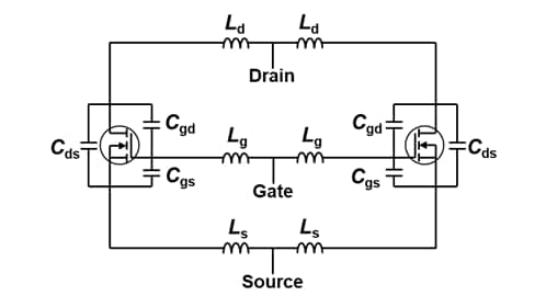
Figure 1. Model equivalent circuit of two MOSFETs connected in parallel 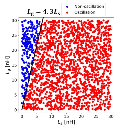
Figure 2. Simulation of oscillation in two MOSFETs with zero gate resistance connected in parallel 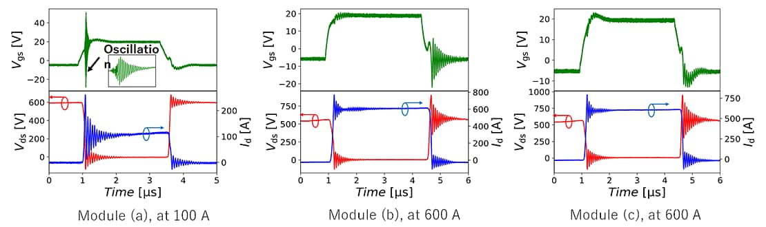
Vgs: Gate-Source voltage, Vds: Drain-Source voltage, Id: Drain current
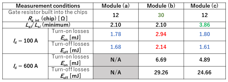
Figure 3. Switching waveforms and switching losses of the prototype modules (Source: Toshiba Group tests) Original – Toshiba
-

MCC introduced the latest additions to its robust portfolio: 10 1200V SiC N-channel MOSFETs in versatile TO-247-4, TO-247-4L, and TO-247AB packages. These new MOSFETs are available in 3-pin and 4-in (Kelvin source) configurations and meet the rising demand for high-power, high-voltage applications.
Boasting exceptional on-resistance values from 21mΩ to 120mΩ (typ.) and fast switching speeds, these components are the ones you can count on for reliable performance. Their excellent thermal properties and fast intrinsic body diode ensure smooth, efficient operation in the most challenging conditions, making them a must-have for critical power systems.
Features & Benefits:
- High-power capability: 1200V MOSFET with SiC technology
- Fast, reliable switching: Intrinsic body diode improves efficiency & ruggedness Enhanced performance: High switching speed with low gate charge
- Wide on-resistance selection: ranging from 21mΩ to 120mΩ (typ.)
- Efficiency: Superior thermal properties and low switching losses
- Durability: Avalanche ruggedness
- Versatility: TO247 3-pin and 4-pin package options
Original – Micro Commercial Components
-

PANJIT introduced latest bridge rectifier packaging: the low-profile GBJA and KBJB. In the ever-evolving world of electronic components, where space efficiency is increasingly in demand, the new low-profile packages offer excellent solutions. When integrated into the PCB, the GBJA can reduce the total height by 34% compared to the GBJ, and the KBJB can reduce it by 36% compared to the KBJ package. This substantial reduction in body height makes them ideal for applications where space is at a premium, responding to the increasing demand for compact and efficient power solutions.
Key Features
Low Body Profile Design: The GBJA and KBJB packages are compact, significantly reducing height without changing pitch angles and body width. When incorporated into the PCB, the GBJA offers a 34% reduction in total height compared to the GBJ, while the KBJB achieves a 36% reduction compared to the KBJ package, offering excellent solutions for space-constrained designs.
Design Compatibility: By keeping the pitch angles and body width the same while just shortening the body height, the new packages remain compatible with the original ones, giving designers the flexibility to either maintain the original PCB layout or shrink the overall design size, including the heatsink. This adaptability ensures easy integration into existing designs and optimizes space utilization for various requirements, while also avoiding the risk of quality issues associated with traditional lead-bending methods to fit the design.Target Applications
GBJA and KBJB series are ideal for high-demand applications where compact power solutions are crucial:
• Slim Power Adapters: Perfect for creating thinner, more portable power adapters.
• Power Supplies for Gaming Consoles: Meet the needs of powerful gaming consoles with sleek, modern designs.
• TV Power Supplies: Ideal for TVs, offering unobtrusive and efficient power solutions.
By adopting the GBJA and KBJB series, manufacturers can create compact, efficient power supplies that meet the growing consumer demand for smaller, portable devices such slim TVs or other modern electronic devices.Bridge Rectifiers in GBJA and KBJB Packages
- KBJB1006
- GBJA1506
- KBJB1008
- GBJA1508
- KBJB1010
- GBJA1510
- KBJB1506
- GBJA2506
- KBJB1508
- GBJA2508
- KBJB1010
- GBJA2510
- GBJA3506
- GBJA3508
- GBJA3510
Original – PANJIT International
-

Power Master Semiconductor has released 2nd generation of the 1200V eSiC MOSFET to meet the requirements of higher efficiency, high power density, robust reliability, and ruggedness in various applications such as DC EV charging stations, solar inverters, energy storage systems (ESS), motor drives and industrial power supplies. 1200V eSiC MOSFETs offer significant system advantages such as higher power density, efficiency and less cooling effort due to its much lower power losses.
Therefore, SiC MOSFETs are gaining popularity especially for renewable energy systems, EV charging systems that required higher power density, efficiency and robustness. DC EV charging station is level-3 charger and its power level is increasing by modular configuration as demand of faster charging time and higher battery capacity of EV. DC EV charging provides a mostly constant current output for wide DC output voltage range (200V to 900V) and load profile.
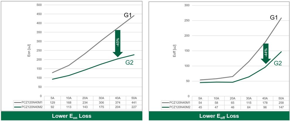
The new generation of 1200V eSiC MOSFET, Gen2 improved key FOM characteristics such as gate charge (QG), stored energy in output capacitance (EOSS), reverse recovery charger (QRR) and output charge (QOSS) by up to 30% compared to previous generation. This new generation SiC MOSFET technology offers significant system advantages such as smaller, lighter, higher efficiency, and less cooling effort thanks to its much lower power losses in various power conversion applications.
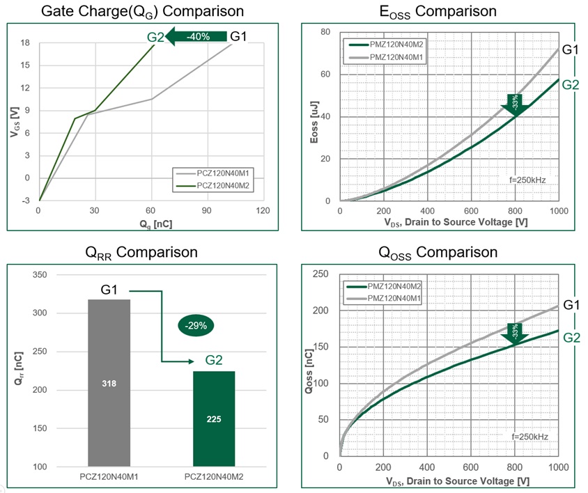
1200V eSiC MOSFET Gen2 offer excellent switching performance and 100% tested avalanche capability. It achieved 44% lower switching loss compared to the previous generation by extremely low miller capacitance (QGD).
Power Master Semiconductor is steadfastly committed to developing cutting-edge power device solutions that prioritize efficiency and sustainability,” said Namjin Kim, Sr. Director Sales & Marketing. “The introduction of our new generation of 1200V eSiC MOSFET marks a substantial leap forward in facilitating the development of cleaner, more efficient power systems. We are confident that the 1200V eSiC Gen2 MOSFET will play a transformative role in high-performance applications.
Original – Power Master Semiconductor
-

In the face of escalating climate crises and a dramatic rise in global energy demands, governments and industries are committing to ambitious climate goals aimed at mitigating environmental impact and securing a sustainable future. Key to these efforts is the transition to electrification to reduce carbon emissions and embrace renewable energy resources.
In a significant step towards accelerating this global transition, onsemi introduced its latest generation silicon carbide technology platform, EliteSiC M3e MOSFETs. The company also disclosed plans to release multiple additional generations through 2030.
“The future of electrification is dependent on advanced power semiconductors. Today’s infrastructure cannot keep up with the world’s demands for more intelligence and electrified mobility without significant innovations in power. This is critical to the ability to achieve global electrification and stop climate change,” said Simon Keeton, group president, Power Solutions Group, onsemi. “We are setting the pace for innovation, with plans to significantly increase power density in our silicon carbide technology roadmap through 2030 to be able to meet the growing demands for energy and enable the global transition to electrification.”
The EliteSiC M3e MOSFETs will play a fundamental role in enabling the performance and reliability of next-generation electrical systems at lower cost per kW, thus influencing the adoption and effectiveness of electrification initiatives. With the ability to operate at higher switching frequencies and voltages while minimizing power conversion losses, this platform is essential for a wide range of automotive and industrial applications such as electric vehicle powertrains, DC fast chargers, solar inverters and energy storage solutions.
Additionally, the EliteSiC M3e MOSFETs will enable the transition to more efficient, higher-power data centers to meet the exponentially increasing energy demands that power a sustainable artificial intelligence engine.
Through onsemi’s unique design engineering and manufacturing capabilities, the EliteSiC M3e MOSFETs achieve a significant reduction in both conduction and switching losses on the trusted and field-proven planar architecture. Compared to previous generations, the platform can reduce conduction losses by 30% and turn-off losses by up to 50%.
By extending the life of SiC planar MOSFETs and delivering industry-leading performance with EliteSiC M3e technology, onsemi can ensure the robustness and stability of the platform, making it a preferred choice for critical electrification applications
The EliteSiC M3e MOSFETs also offer the industry’s lowest specific on-resistance (RSP) with short circuit capability which is critical for the traction inverter market that dominates SiC volume. Packaged in onsemi’s state-of-the-art discrete and power modules, the 1200V M3e die delivers substantially more phase current than previous EliteSiC technology, resulting in approximately 20% more output power in the same traction inverter housing. Conversely, a fixed power level can now be designed with 20% less SiC content, saving costs while enabling the design of smaller, lighter and more reliable systems.
Additionally, onsemi provides a broader portfolio of intelligent power technologies including gate drivers, DC-DC converters, e-Fuses and more to pair with the EliteSiC M3e platform. The end-end onsemi combination of optimized, co-engineered power switches, drivers and controllers enable advanced features via integration, lowering overall system cost.
Global energy demands are projected to soar over the next decade, making the need for increased power density in semiconductors paramount. onsemi is leading innovation across its silicon carbide roadmap – from die architectures to novel packaging techniques – that will continue to address the general industry demand for increased power density.
With each new generation of silicon carbide, cell structures will be optimized to efficiently push more current through a smaller area, increasing power density. When coupled with the company’s advanced packaging techniques, onsemi will be able to maximize performance and reduce package size.
By applying the concepts of Moore’s Law to the development of silicon carbide, onsemi can develop multiple generations in parallel and accelerate its roadmap to bring several new EliteSiC products to market at an accelerated pace through 2030.
“We are applying our decades of experience in power semiconductors to push the boundaries of speed and innovation in our engineering and manufacturing capabilities to meet the rising global energy demands,” said Dr. Mrinal Das, senior director of technical marketing, Power Solutions Group, onsemi. “There is a huge technical interdependency between the materials, device and package in silicon carbide. Having full ownership over these key aspects allows us to have control over the design and manufacturing process and bring new generations to market much faster.”
The EliteSiC M3e MOSFET in the industry-standard TO-247-4L package is now sampling.
Original – onsemi
-

Toshiba Electronics Europe GmbH added two new 150V N-channel power MOSFET products based upon their latest generation U-MOS X-H Trench process. The TPH1100CQ5 and TPH1400CQ5 devices are designed specifically for use in high-performance switching power supplies, such as those used in data centres and communication base stations as well as other industrial applications.
With a maximum drain-source voltage (VDSS) rating of 150V and drain current (ID) handling 49A (TPH1100CQ5) and 32A (TPH1400CQ5), the new devices feature a maximum drain-source on-resistance RDS(ON).
The new products offer improved reverse recovery characteristics that are critical in synchronous rectification applications. In the case of TPH1400CQ5, the reverse recovery charge (Qrr) is reduced by approximately 73% to 27nC (typ.) and the reverse recovery time (trr) of 36 ns (typ.) is approximately 45% faster compared with Toshiba’s existing TPH1400CQH, which offers the same voltage and RDS(ON).
Used in synchronous rectification applications, the TPH1400CQ5 reduces the power loss of switching power supplies and helps improve efficiency. If the device is used in a circuit that does not operate in reverse recovery mode, the power loss is equivalent to that of the TPH1400CQH.
When used in a circuit that operates in reverse recovery mode, the new products reduce spike voltages generated during switching, helping to improve EMI characteristics of designs, and reducing the need for external filtering. The devices are housed in a versatile, surface-mount SOP Advance(N) package measuring just 4.9mm x 6.1mm x 1.0mm.
To support designers, Toshiba has developed a G0 SPICE model for rapid verification of the circuit function as well as highly accurate G2 SPICE models, for accurate reproduction of transient characteristics.
Shipments of the new devices start today, and Toshiba will continue to expand their lineup of power MOSFETs that help improve equipment efficiency.
Original – Toshiba
-

Toshiba Electronic Devices & Storage Corporation launched 650V N-channel power MOSFETs “TK068N65Z5, TK095E65Z5, TK095A65Z5, TK095V65Z5, TK115E65Z5, TK115A65Z5, TK115V65Z5 and TK115N65Z5” and added them to the lineup of Toshiba’s latest-generation DTMOSVI series with high-speed diodes (DTMOSVI (HSD)) that uses super junction structure and is suitable for high-efficiency switching power supplies for data centers and power conditioners for photovoltaic generators. Packages of the new products are TO-247, TO-220SIS, TO-220 and DFN8×8.
The new products with the DTMOSVI (HSD) process use high-speed diodes to improve the reverse recovery characteristics important for bridge circuit and inverter circuit applications. Against Toshiba’s existing product TK090A65Z of the standard type DTMOSVI, the new product TK095A65Z5 achieves an approximately 65% reduction in reverse recovery time (trr), and an approximately 88% reduction in reverse recovery charge (Qrr) (measurement conditions: -dIDR/dt=100A/μs).
In addition, the DTMOSVI (HSD) process improves on the reverse recovery characteristics of Toshiba’s existing products DTMOSIV series with high-speed diodes (DTMOSIV (HSD)), and has a lower drain cut-off current at high temperatures. Furthermore, the figure of merit “drain-source On-resistance × gate-drain charge” is also lower.
The high temperature drain cut-off current of the new product TK095A65Z5 is approximately 91% lower, and the drain-source On-resistance × gate-drain charge approximately 70% lower, than in Toshiba’s existing product TK35A65W5. This advance will cut equipment power loss and help to improve efficiency.
A reference design, “1.6kW Server Power Supply (Upgraded)“, that uses the same series product TK095N65Z5 is available on Toshiba’s website.
Toshiba also offers tools that support circuit design for switching power supplies. Alongside the G0 SPICE model, which verifies circuit function in a short time, highly accurate G2 SPICE models that accurately reproduce transient characteristics are now available.
Toshiba also will continue to expand its lineup of the DTMOSVI series. This will enhance switching power supply efficiency, contributing to energy-saving equipment.
Applications
Industrial equipment
- Switching power supplies (data center servers, communications equipment, etc.)
- EV charging stations
- Power conditioners for photovoltaic generators
- Uninterruptible power systems
Features
- MOSFETs with high-speed diodes in the latest-generation DTMOSVI series
- Reverse recovery time due to high-speed diodes:
TK068N65Z5 trr=135ns (typ.)
TK095E65Z5, TK095A65Z5, TK095V65Z5 trr=115ns (typ.)
TK115E65Z5, TK115A65Z5, TK115V65Z5, TK115N65Z5 trr=110ns (typ.) - High-speed switching time due to low gate-drain charge:
TK068N65Z5 Qgd=22nC (typ.)
TK095E65Z5, TK095A65Z5, TK095V65Z5 Qgd=17nC (typ.)
TK115E65Z5, TK115A65Z5, TK115V65Z5, TK115N65Z5 Qgd=14nC (typ.)
Original – Toshiba
-

Nexperia released 650V ultra- and hyperfast recovery rectifiers in D2PAK Real-2-Pin (R2P) packaging for use in various automotive, industrial and consumer applications including charging adapters, photovoltaic (PV), inverters, servers and switched mode power supplies (SMPS).
Combining planar die technology with a state-of-the-art junction termination (JTE) design, these rectifiers offer high power density, fast switching times with soft recovery and excellent reliability. They are encapsulated in a D2PAK Real-2-Pin Package (SOT8018), which offers the same package outline as the standard D2PAK package but has only two pins instead of three (the middle cathode pin has been removed). This increases the pin-to-pin distance from 1.25mm to over 4mm, which allows to meet the creepage and clearance requirements stated in the IEC 60664 standard.
“These recovery rectifiers further demonstrate Nexperia’s expertise in the field of semiconductor device packaging” according to Frank Matschullat, Head of Product Group Power Bipolar Discretes at Nexperia. “By taking the innovative step of removing the cathode pin from a standard D2PAK package, Nexperia has created a Real-2-Pin package that can meet the creepage and clearance requirements, in particular for high voltage automotive applications.”
Original – Nexperia
-
Vishay Intertechnology, Inc. introduced 16 new Gen 3 1200 V silicon carbide (SiC) Schottky diodes. Featuring a merged PIN Schottky (MPS) design, the Vishay Semiconductors devices combine high surge current robustness with low forward voltage drop, capacitive charge, and reverse leakage current to increase efficiency and reliability in switching power designs.
The next-generation SiC diodes released today consist of 5 A to 40 A devices in the TO-220AC 2L, TO-247AD 2L, and TO-247AD 3L through-hole and D2PAK 2L (TO-263AB 2L) surface-mount packages. The diodes offer a low capacitance charge down to 28 nC, while their MPS structure — which features a backside thinned via laser annealing technology — delivers a reduced forward voltage drop of 1.35 V. In addition, the devices’ low typical reverse leakage current down to 2.5 µA at 25 °C reduces conduction losses, ensuring high system efficiency during light loads and idling. Unlike ultrafast diodes, the Gen 3 devices have virtually no recovery tail, which further improves efficiency.
Typical applications for the diodes will include AC/DC PFC and DC/DC ultra high frequency output rectification in FBPS and LLC converters for solar power inverters; energy storage systems; industrial drives and tools; and datacenters. For the harsh environments of these applications, the devices combine operating temperatures to +175 °C with forward surge ratings to 260 A for high robustness. In addition, diodes in the D2PAK 2L package feature a molding compound with a high CTI ≥ 600, ensuring excellent electrical insultation at elevated voltages.
Offering high reliability, the RoHS-compliant and halogen-free devices have passed higher temperature reverse bias (HTRB) testing of 2000 hours and temperature cycling testing of 2000 thermal cycles.
Device Specification Table:
Part # IF(AV) (A) IFSM (A) VF at IF (V) QC (nC) Configuration Package VS-3C05ET12T-M3 5 42 1.35 28 Single TO-220AC 2L VS-3C10ET12T-M3 10 84 1.35 55 Single TO-220AC 2L VS-3C15ET12T-M3 15 110 1.35 81 Single TO-220AC 2L VS-3C20ET12T-M3 20 180 1.35 107 Single TO-220AC 2L VS-3C05ET12S2L-M3 5 42 1.35 28 Single D2PAK 2L VS-3C10ET12S2L-M3 10 84 1.35 55 Single D2PAK 2L VS-3C15ET12S2L-M3 15 110 1.35 81 Single D2PAK 2L VS-3C20ET12S2L-M3 20 180 1.35 107 Single D2PAK 2L VS-3C10EP12L-M3 10 84 1.35 55 Single TO-247AD 2L VS-3C15EP12L-M3 15 110 1.35 81 Single TO-247AD 2L VS-3C20EP12L-M3 20 180 1.35 107 Single TO-247AD 2L VS-3C30EP12L-M3 30 260 1.35 182 Single TO-247AD 2L VS-3C10CP12L-M3 2 x 5 42 1.35 28 Common cathode TO-247AD 3L VS-3C20CP12L-M3 2 x 10 84 1.35 55 Common cathode TO-247AD 3L VS-3C30CP12L-M3 2 x 15 110 1.35 81 Common cathode TO-247AD 3L VS-3C40CP12L-M3 2 x 20 180 1.35 107 Common cathode TO-247AD 3L Samples and production quantities of the new SiC diodes are available now, with lead times of 13 weeks.
Original – Vishay Intertechnology
-
Infineon Technologies AG introduced the new CoolGaN™ Transistor 700 V G4 product family. The devices are highly efficient for power conversion in the voltage range up to 700 V. In contrast to other GaN products on the market, the input and output figures-of-merit of these transistors provide a 20 percent better performance, resulting in increased efficiency, reduced power losses, and more cost-effective solutions. The combination of electrical characteristics and packaging ensures maximum performance in many applications such as consumer chargers and notebook adapters, data center power supplies, renewable energy inverters, and battery storage.
The product series comprises 13 devices with a voltage rating of 700 V and on-resistance range from 20 mΩ to 315 mΩ. The increased granularity in device specification, combined with a wide range of industry standard package options including PDFN, TOLL and TOLT allow R DS resistance and packages to be selected according to application requirements. As a result, both electrical and thermal system performance can be optimized and implemented in the most cost-effective solution.
The devices are characterized by a fast turn-on and turn-off speed and minimal switching losses. The on-resistance range enables power systems from 20 W to 25,000 W. In addition, the 700 V E-mode with the industry’s highest transient voltage of 850 V increases the reliability of the overall system as it offers greater robustness against anomalies in the user environment such as voltage peaks.
The CoolGaN Transistor 700 V G4 products in TOLL, PDFN 5×6 and 8×8 packages are available now, more variety in R DS(on) as well as the TOLT package will follow later this year.
Original – Infineon Technologies
