-
 LATEST NEWS / PROJECTS / SiC / TOP STORIES / WBG
SiCrystal’s SiC Wafers Production Capacity to Triple by 2027 with a New Production Site in Nuremberg
July 4, 2024
2 Min ReadIn an important step towards strengthening the semiconductor industry and promoting sustainable technologies, SiCrystal GmbH will create new, additional production space in the north-east of Nuremberg, directly opposite the existing site. The new building will offer an additional 6,000 square meters of production space and will be equipped with state-of-the-art technology to further optimize the production of silicon carbide wafers.
The close proximity to the existing plant will ensure close integration of the production processes. SiCrystal’s total production capacity, including the existing building, will be approximately three times higher in 2027 than in 2024.
“The new space will significantly increase the production capacity for SiC substrates and we are proud that we were able to welcome Mayor König to the ground-breaking ceremony,” says Dr. Robert Eckstein, CEO of SiCrystal. This underlines the importance of this project for the city and the region.
“This groundbreaking ceremony marks an important milestone for SiCrystal and underlines our commitment to the metropolitan region. In this way, we can continue to supply innovative products of the highest quality for our customers in the future and make a positive contribution to global sustainability. “, said Dr. Erwin Schmitt, COO of SiCrystal. “With the additional production capacities, we will strengthen our market position and make an important contribution to technological development in the semiconductor industry.”
Nuremberg’s Mayor Marcus König congratulates on this event: “SiCrystal is one of the world’s leading manufacturers of silicon carbide semiconductor substrates – among other things, these products are needed for the energy transition. I am delighted that SiCrystal is committing itself to Nuremberg as a location with this massive investment and is thus not only retaining jobs but also creating new ones. Nuremberg is an attractive location.”
The construction work is scheduled to be completed by the beginning of 2026. And will create new jobs in the region. The new building is being realized in cooperation with the general contractor Systeambau from Hilpoltstein.
SiC wafers from SiCrystal, a subsidiary of the Japanese ROHM Group, are of crucial importance for the production of high-performance semiconductor components. By using SiC, we can achieve higher efficiency, lower energy consumption and improved performance in various applications such as electric vehicles, solar energy, and industrial equipment.
SiCrystal is proud to be a fast-growing employer in the metropolitan region and aims to increase employment by more than 100 by the end of the 2027/28 financial year.
Original – SiCrystal
-
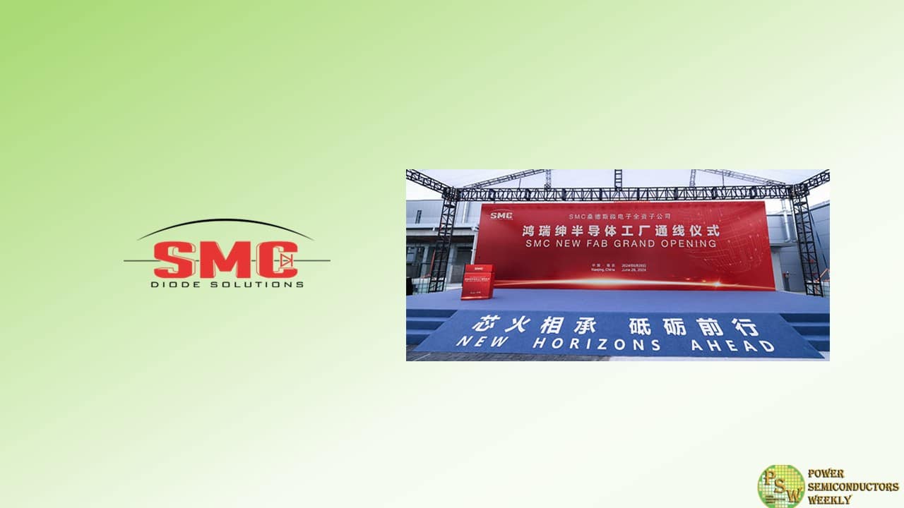
SMC Diode Solutions, an American-led semiconductor design and manufacturing company, celebrated the opening of its second power discrete fab in Nanjing, China. The new facility realized volume production only 21 months after groundbreaking in September of 2022, and will begin shipments to customers in Q4 2024 for high power and high voltage rectifiers and MOSFET 6-inch and 8-inch wafers.
This new fab marks a milestone in SMC’s growth as they further invest in the China market and the growing renewable energy sector. The new 300,000 square foot facility is set to produce 1.2 million silicon wafers and 60,000 silicon carbide wafers per year, increasing SMC’s total production by over four times. SMC’s current fab in Lukou, Nanjing currently produces 300,000 silicon wafers per year. The $3 billion RMB investment in the new fab will allow SMC to handle the end-to-end production of silicon carbide products for the first time and has created three hundred new jobs.
“As the world moves towards using more and more renewable energy, we are thrilled to now be able to participate in the sector and be part of the solution to increase green energy usage and protect our Earth. We are very excited to have our new fab up and running and we look forward to servicing our customers’ needs better with the increased capacity.” – Dr. Yunji Corcoran, SMC chairwoman and chief executive officer.
As Nanjing is also home to SMC’s current fab, the city was an advantageous choice for the new fab location. With their experienced management team, starting up the new fab was a seamless process, allowing production to begin not long after breaking ground. The city is also home to abundant resources and engineering talent, making it an ideal place for SMC to grow and expand.
Power Semiconductors Weekly team had pleasure to interview Dr. Yunji Corcoran on this occasion:
- The company history dates back to 1997. Can you tell us about some of the major milestones and your semiconductor journey so far?
Certainly. In the early stages of our company, from 1997 until about 2014, we focused on the US and South Korean markets. We were growing steadily, but remained focused on the quality of our products. From 2014 to 2019, we began to focus on active growth, but I consider this more of a preparation stage for our company’s expansion. We investigated ways to create better products and put more of our R&D efforts into new silicon and Silicon Carbide (SiC) products. We also began strengthening our salesforce globally. From 2019 on, we started shipping our new products, both silicon and SiC. Now, we have reached our most significant milestone to date: opening our second fab and quadrupling our production capabilities. We are beginning a new phase that will focus on growing our presence in the power semiconductor market.
- Today we see many semiconductor companies investing a lot of energy into the automotive, renewables, and AI applications. With a wide product line and a new wafer fab to support further expansion, what are your major areas of interest and how do you see them evolve in the coming years?
Automotive, renewables, and AI are extremely relevant markets for both our company and the overall semiconductor industry right now. AI requires a lot of power supply, so we plan to grow our power supply products in that area alongside our existing customers. Automotive and renewables are newer segments for us and the semiconductor market, but ones with incredibly high demand right now. The market is growing rapidly, so we are growing with aims to successfully compete in those areas as well.
Our plan is to focus on our growth within the power supply market and naturally expand into the sustainable energy market. As the world continues to prioritize clean energy, the demand for EV and renewable energy products will also grow. Since SiC products in particular meet the specific power needs of those applications, a rise in the use of SiC products seems likely. I suspect the semiconductor industry will play a crucial role in providing more clean energy globally, which we are excited to be a part of.
- With the new fab you plan to address both silicon and silicon carbide markets? What is your view on the growing demand for SiC and how SMC Diode Solutions plan to correspond to it?
Yes, our new fab will produce both silicon and SiC products. Our current fab produces approximately 300,000 silicon wafers per year, but our new fab has the capability to produce a total of 1,260,000 wafers per year – 1,200,000 silicon and 60,000 SiC. We are very much focused on our silicon power products and view our SiC line as a natural extension of that.
The growing demand for SiC products makes perfect sense. SiC is a material with remarkable properties. It is considered a “wide bandgap” material, which means that it requires more energy to excite electrons from the valence band to the conduction band compared to standard silicon semiconductors. As a result, it offers superior performance characteristics including higher reverse voltage capabilities and greater stability at high temperatures.
Overall, SiC-based products offer improved efficiency and reliability compared to traditional silicon counterparts. For a lot of newer applications, particularly in the sustainable energy sector, these capabilities have become more and more necessary. We see our new fab opening as a natural response to this demand, ande are increasing our capabilities to grow alongside the market.
- Today you have four major locations in China, South Korea, Germany and the USA. Do you plan to expand your network further?
Yes, definitely. We consider SMC to be a global company, and have a range of operations throughout the world, including our headquarters in China and other offices in the US, Germany, South Korea, the UK, and India. As we grow and gain customers throughout the world, we will continue to establish more locations, whether they are R&D, manufacturing, packaging, or sales offices.
- Speaking of the network and future growth opportunities. Both of your fabs are located in Nanjing. With many companies in the US already taking advantage of the CHIPS and Science Act, do SMC Diode Solutions have any considerations to join the rest and use this chance to strengthen the US presence?
It is exciting that governments are recognizing the importance of semiconductors through initiatives like the CHIPS and Science Act, and I think this will really bolster the industry as a whole. Right now, we’re focused on our manufacturing efforts in Asia, but are open to the possibility as we continue to grow.
- With the rise of the Chinese semiconductor industry and a very competitive landscape, how do you position your company and differentiate from the growing number of new entrants?
The key thing is our products. Our products stand out for their high quality and outstanding performance. Our team’s commitment to customer service really sets us apart as well.
Our company also approaches the semiconductor market from a unique perspective. As a business with global locations and leadership, we deeply understand the needs of the international market. We prioritize high quality standards that the international market demands while benefiting from relatively low overall production costs, creating an ideal product for our customers.
- We see many companies in China, Europe, the US, shifting to the vertical structure and full integration of all processes – from growing the semiconductor boules to the packaging of the final product. What are your thoughts on such an approach and do you see it applicable for your company in the future as well?
I’ve also noticed this trend in the industry. While I can see the benefits of this approach for some, I would not anticipate applying it within SMC. I believe in focusing our efforts on what we’re able to do best. We have specialized in design and manufacturing for over 25 years and plan to continue that.
We do have an existing silicon module line, so we are considering expanding into SiC modules in the future. However, for our company we believe it’s best to stay focused on the functions we currently have and prioritize delivering the highest quality product.
- And lastly, after the announcement of a new fab opening, many of your partners would be willing to engage in discussions to find out more. What trade shows or conferences in the second half of 2024 can they meet the company at?
We would love to engage in those discussions as well. You can find us with our own booth at Electronica 2024 this September in Munich, Germany and the Anaheim Electronics & Manufacturing Show (AEMS 2024) in Anaheim, California this October. We will also be attending ISCRM 2024 in Raleigh, North Carolina this fall.
More often than not, you will find someone from our company at any major semiconductor event. Feel free to contact us at sales@smc-diodes.com for any questions or check our website updates to see where you can find us next.
Original – SMC Diode Solutions
-
Semiconductor manufacturer Nexperia announced plans to invest USD 200 million (appx. 184 million Euros) to develop the next generation of wide bandgap semiconductors (WBG) such as silicon carbide (SiC) and gallium nitride (GaN), and to establish production infrastructure at the Hamburg site. At the same time, wafer fab capacity for silicon (Si) diodes and transistors will be increased. The investments are jointly announced with Hamburg’s Minister for Economic Affairs, Dr. Melanie Leonhard, on the occasion of the 100-year anniversary of the production site.
To meet the growing long-term demand for efficient power semiconductors, all three technologies (SiC, GaN, and Si) will be developed and produced in Germany starting in June 2024. This means Nexperia is supporting key technologies in the fields of electrification and digitalization. SiC and GaN semiconductors enable power-hungry applications, such as data centers, to operate with exceptional efficiency and are core building blocks for renewable energy applications and electromobility. These WBG technologies have great potential and are increasingly important for achieving decarbonization goals.
“This investment strengthens our position as a leading supplier of energy-efficient semiconductors and enables us to utilize available electrical energy more responsibly,” comments Achim Kempe, COO and managing director at Nexperia Germany. “In the future, our Hamburg fab will cover the complete range of WBG semiconductors while still being the largest factory for small signal diodes and transistors. We remain committed to our strategy of producing high-quality, cost-efficient semiconductors for standard applications and power-intensive applications, while addressing one of the greatest challenges of our generation: meeting the growing demand for energy and while reducing the environmental footprint.”
First production lines for high-voltage GaN D-Mode transistors and SiC diodes started in June 2024. The next milestone will be modern and cost-efficient 200 mm production lines for SiC MOSFETs and GaN HEMTs. These will be established at the Hamburg factory over the next two years. At the same time, the investment will help to further automate the existing infrastructure at the Hamburg site and expand silicon production capacity by systematically converting to 200 mm wafers. Following the expansion of the clean room areas, new R&D laboratories are being built to continue to ensure a seamless transition from research to production in the future.
In addition to advancing technology, the semiconductor supplier expects the initiative to stimulate local economic development. The investments make an important contribution to securing and creating jobs and enhancing the European Union’s semiconductor self-sufficiency. Nexperia works closely with universities and research institutes to benefit from each other’s expertise and promote highly qualified employee training. Nexperia relies on a robust research and development ecosystem in Hamburg and throughout Europe. Development partnerships and co-operations, e.g. in the field of GaN technology as part of the Industrial Affiliation Program (IIAP) of the nanoelectronics research center imec, play a crucial role. These and other collaborations ensure continuous innovation and technological excellence in Nexperia’s products.
“The planned investment enables us to bring WBG chip design and production to Hamburg. However, SiC and GaN are by no means new territory for Nexperia. GaN FETs have been part of our portfolio since 2019, and in 2023 we expanded our range of products to include SiC diodes and SiC MOSFETs, the latter in collaboration with Mitsubishi Electric. Nexperia is one of the few suppliers to offer a comprehensive range of semiconductor technologies, including Si, SiC, and GaN in both e-mode and d-mode. This means, we offer our customers a one-stop shop for all their semiconductor needs”, explains Stefan Tilger, CFO and managing director at Nexperia Germany.
The investment is yet another milestone in the 100-year history of Nexperia’s production site in Hamburg-Lokstedt. Since the foundation of Valvo Radioröhrenfabrik in 1924, the site has continuously developed and today supplies around a quarter of the global demand for small signal diodes and transistors. Since its spin-off from NXP in 2017, Nexperia has invested substantial sums in the Hamburg site, increased the workforce from 950 to around 1,600 and brought the technological infrastructure up to the state-of-the-art. This continued expenditure underlines the company’s commitment to remaining at the forefront of the industry and providing innovative solutions to its customers worldwide.
Original – Nexperia
-
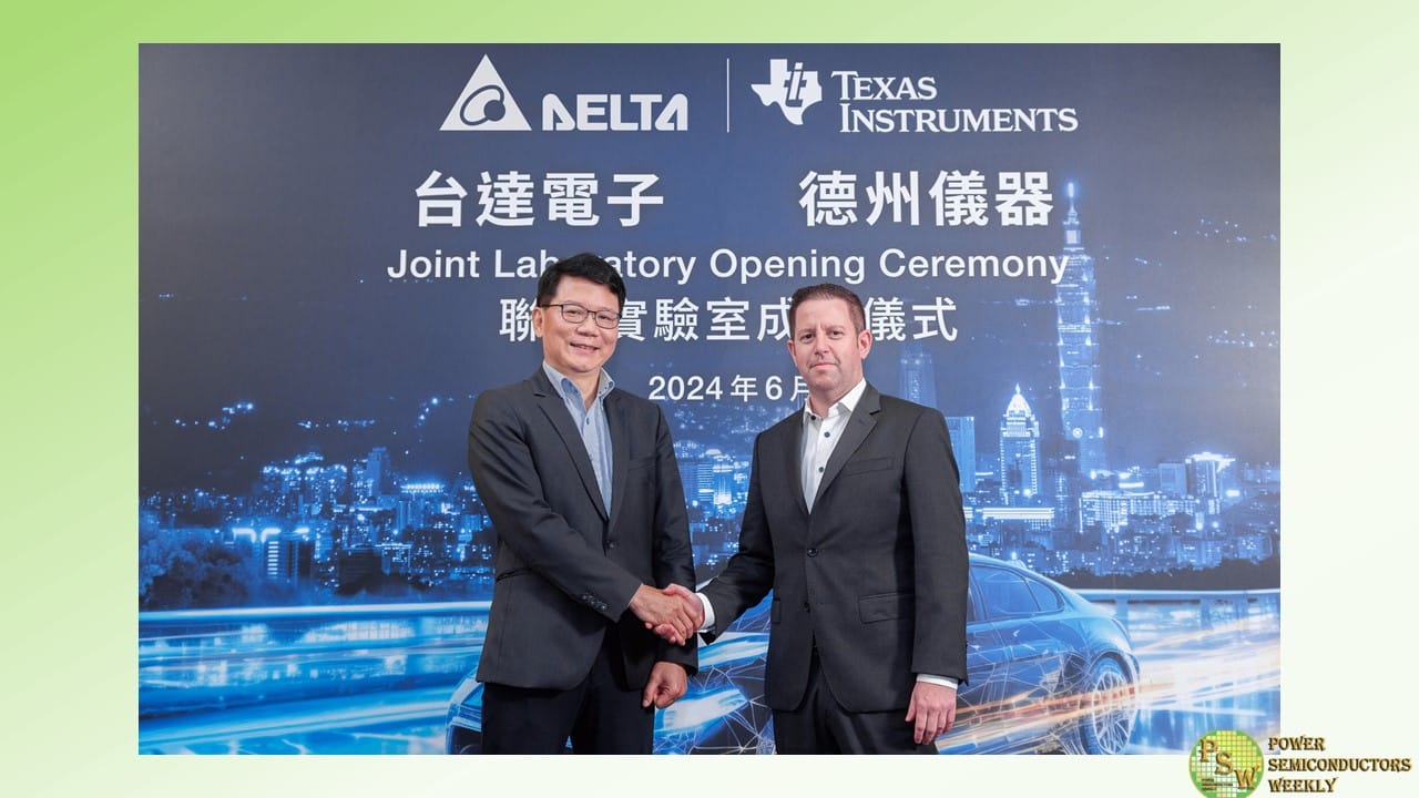
Texas Instruments announced a long-term collaboration with Delta Electronics, a global power and energy management manufacturer, to create next-generation electric vehicle (EV) onboard charging and power solutions. This work will leverage both companies’ research and development capabilities in power management and power delivery in a joint innovation laboratory in Pingzhen, Taiwan. Together, TI and Delta aim to optimize power density, performance and size to accelerate the realization of safer, faster-charging and more affordable EVs.
“The transition to electric vehicles is key to helping achieve a more sustainable future, and through years of collaboration with Delta Electronics, we have a solid foundation to build upon,” said Amichai Ron, senior vice president for Embedded Processing at TI. “Together with Delta, we will use TI semiconductors to develop EV power systems like onboard chargers and DC/DC converters that are smaller, more efficient and more reliable, increasing vehicle driving range and encouraging more widespread adoption of electric vehicles.”
“Delta has been developing high-efficiency automotive power products, systems and solutions since 2008 to help reduce transportation-related carbon emissions,” said James Tang, executive vice president of Mobility and head of the Electric Vehicle Solutions business group at Delta Electronics.
“Through the establishment of this joint innovation laboratory with TI, Delta intends to leverage TI’s abundant experience and advanced technology in digital control and GaN to enhance the power density and performance of our EV power systems. With more leading-edge product development and design capabilities, we aim to achieve closer technology exchange and collaboration to accelerate product development and improve product safety and quality. We look forward to furthering our technology leadership and creating a win-win situation in the rapidly developing electric vehicle market.”
Three phases of development for next-generation automotive power solutions
- Phase one for the collaboration focuses on Delta’s development of a lighter-weight, cost-effective 11kW onboard charger, using TI’s latest C2000™ real-time microcontrollers (MCUs) and TI’s proprietary active electromagnetic interference (EMI) filter products. The companies are working together using TI’s products to reduce the charger’s size by 30% while achieving up to 95% power conversion efficiency.
- In phase two, TI and Delta will leverage the latest C2000 real-time MCUs for automotive applications to enable automakers to achieve automotive safety integrity levels (ASILs) up to ASIL D, which represents the strictest automotive safety requirements. Highly integrated automotive isolated gate drivers will further enhance the power density of onboard chargers, while also minimizing overall solution size.
- In phase three, the two companies will collaborate to develop the next generation of automotive power solutions, capitalizing on TI’s more than 10 years of experience in developing and manufacturing products with gallium nitride (GaN) technology.
“The rapid growth of electronics in automotive applications has enabled more feature-rich, efficient and safer vehicles. However, technical challenges remain,” said Luke Lee, president of Taiwan, Japan, Korea and South Asia, Texas Instruments. “Having been in Taiwan for 55 years, coupled with decades of experience in automotive power management, TI has built a strong connection with the local automotive industry. Establishing this collaboration and joint innovation laboratory with Delta is just one more way TI is driving vehicle electrification forward.”
Original – Texas Instruments
-

Electrification, renewables and artificial intelligence are global megatrends converging and driving unprecedented demands for advanced power semiconductors capable of optimizing energy conversion and management. In a strategic move toward addressing these demands, onsemi announced plans to establish a state-of-the-art, vertically integrated silicon carbide (SiC) manufacturing facility in the Czech Republic. The site would produce the company’s intelligent power semiconductors that are essential for improving the energy efficiency of applications in electric vehicles, renewable energy and AI data centers.
“Our brownfield investment would establish a Central European supply chain to better service our customers’ rapidly increasing demand for innovative technologies that improve the energy efficiency in their applications,” said Hassane El-Khoury, president and CEO, onsemi. “Through a close collaboration with the Czech government, the expansion would also enhance our production of intelligent power semiconductors that are essential to helping ensure the European Union is able to achieve its ambitions to significantly reduce carbon emissions and environmental impact.”
“onsemi’s decision to expand in Czechia is a clear confirmation of our country’s attractiveness for foreign investment and will bring significant momentum for the development of our economy,” said Mr. Jozef Síkela, Minister of Industry and Trade of the Czech Republic. “This investment not only strengthens our position in the semiconductor field but can also contribute to the development of the automotive industry and help us with its adaptation to the rise of electromobility.”
onsemi’s plan to expand SiC manufacturing with a multi-year brownfield investment of up to $2 billion (44 billion CZK) is part of the company’s previously disclosed long-term capital expenditure target. This investment would build on the company’s current operations in the Czech Republic, which include silicon crystal growth, silicon and silicon carbide wafer manufacturing (polished and EPI) and a silicon wafer fab. Today, the site can produce more than three million wafers annually, including more than one billion power devices. Upon completion, the operation would contribute annually more than $270 million USD (6 billion CZK) to the country’s GDP.
Pending all final regulatory and incentive approvals, including the investment incentive approval by the government of the Czech Republic and its notification to the European Commission, this would be one of the largest private sector investments in the Czech Republic’s history and would further contribute to the prosperity and economic dynamism of the Zlín region. onsemi is one of the first companies to invest in advanced semiconductor manufacturing in the Central European region.
With this investment, the company would contribute to the strategic positioning of the region within the EU’s semiconductor value chain and demonstrate that all EU countries can benefit from the European Chips Act. The announcement also reflects onsemi’s strategic alignment with the overarching goals of the European Chips Act of increasing market share and technological advancement to strengthen the resilience of the EU’s semiconductor supply chains in times of ever-growing demand.
Silicon carbide is a critical material for high-power, high-temperature applications, and is extremely difficult to produce. onsemi is one of the only companies in the world with the ability to manufacture SiC-based semiconductors from crystal growth to advanced packaging solutions. By expanding its production facilities in the Czech Republic, onsemi would be faster to provide supply assurance for customers, strengthening its leadership in intelligent power solutions. This integration would also enable onsemi to leverage its latest advancements in research and development (R&D) to maximize manufacturing and production efficiency.
Original – onsemi
-
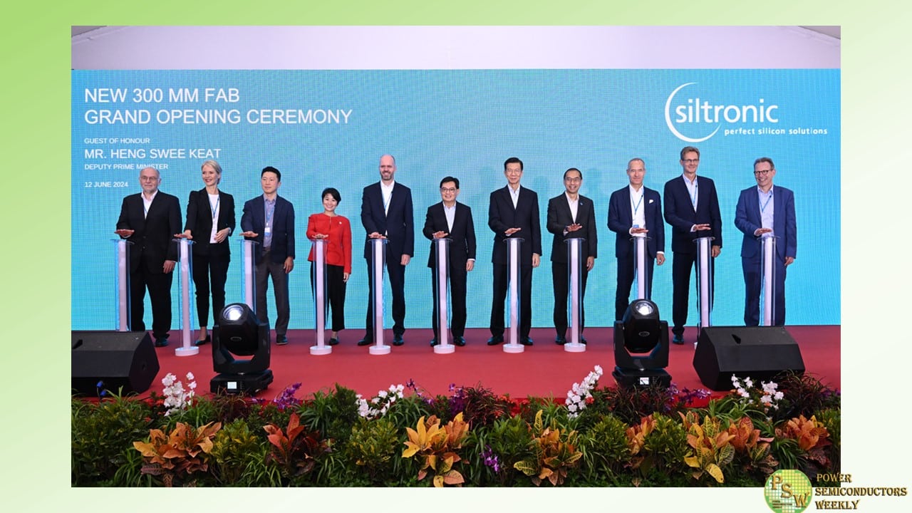
June 12 marked a milestone in the history of Siltronic AG: after more than 500 construction days and roughly 23 million working hours, Siltronic inaugurated one of the world’s most advanced wafer fabs. The inauguration of the new production facility, which is one of the most modern and cost-efficient of its kind, took place in Singapore.
The highly automated fab at JTC’s Tampines Wafer Fab Park was officially opened in the presence of around 150 guests, including numerous high-ranking representatives of the Singaporean government, customers and suppliers. Singapore’s Deputy Prime Minister Heng Swee Keat was the Guest of Honour to grace the occasion. The fab was commissioned at the beginning of 2024 and will now be ramped to full capacity over several years.
“With our new fab, we will accompany the future growth of the wafer industry for many years to come and take Siltronic to a new level. What the entire team, including all business partners, has achieved is a masterpiece, and I would like to thank everyone for their outstanding contribution,” said Dr. Michael Heckmeier, CEO of Siltronic AG, in his speech.
Ms. Jacqueline Poh, Managing Director of Singapore Economic Board (EDB) said: “We are proud of our long-standing partnership with Siltronic. As one of top 5 global wafer suppliers, Siltronic’s new fab is a significant expansion that not only supplies to Singapore’s semiconductor industry but also strengthens the resilience of the global semiconductor supply chain. This investment will create good jobs and further grow the existing collaboration that Siltronic has with local suppliers in automation and precision components.”
The success story of Siltronic in Singapore began in 1997 with the founding of Siltronic Singapore Pte. Ltd. in JTC’s Tampines Wafer Fab Park. The first 200 mm wafers were produced as early as 1999. This was followed in 2006 by the establishment of a joint venture with Samsung and the start of construction of the first 300 mm fab, from which the first wafers were delivered to customers in 2008. The foundation stone for the second 300 mm fab was laid in 2021, and it was officially opened today. Singapore is Siltronic’s largest production site.
Today’s inauguration of the state-of-the-art wafer fab in Singapore is not only the largest investment in Siltronic’s history, but also a milestone of which Siltronic is extremely proud. With its high level of automation and impressive efficiency, the fab sets new standards in our industry and strengthens Siltronic’s position as one of the world’s leading wafer manufacturers.
Original – Siltronic
-
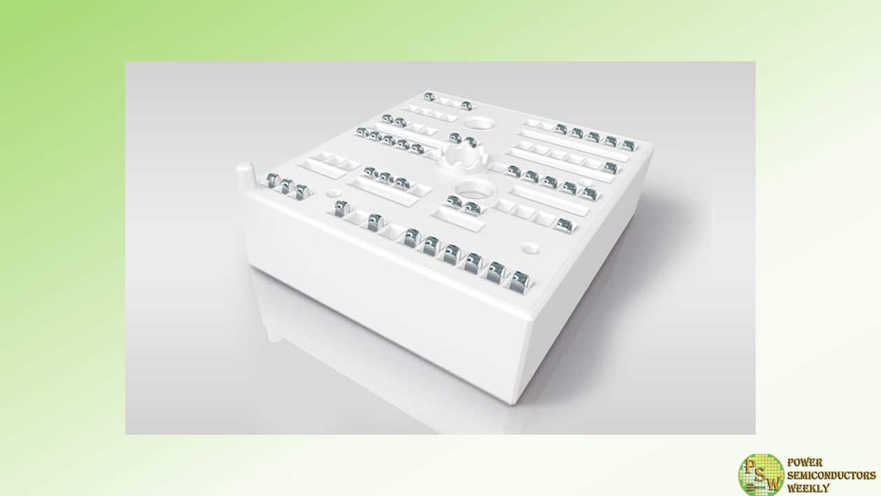
Semikron Danfoss and Vincotech announced the renewal of their cooperation agreement for power semiconductor module packaging. The two enterprise’s alliance, dating back to 2003, has been extended to further strengthen MiniSKiiP packaging technology.
This move underscores Semikron Danfoss and Vincotech’s commitment to advancing MiniSKiiP and delivering cutting-edge solutions that meet the needs of the power electronics industry.
“The partnership with Vincotech is key to ensuring the safe supply of our number one motor drive module MiniSKiiP to our customers,” said Peter Sontheimer, Senior Vice President Industry Division at Semikron Danfoss. “We strongly believe that this type of arrangement is beneficial to the long-term health of the power electronics supply chain.”
Multiple source options for the package to further mitigate the supply chain risk, as well as standards-compliant design, are just a few of the benefits of this renewed cooperation agreement. Engineered for easy assembly and featuring service-friendly spring contacts, MiniSKiiP’s unique hardware has earned an excellent reputation for efficiency and performance in general purpose and servo motor drives.
“We are delighted to be renewing our partnership with Semikron Danfoss for the MiniSKiiP package technology,” said Edoardo Guiotto, VP Sales & Marketing at Vincotech. “This agreement reaffirms our dedication to deliver premium products to our customers and drive innovation and advances in power electronics.”
Semikron Danfoss and Vincotech are now set to take MiniSKiiP’s reliability and standardization to the next level. Customers can look forward this technology bringing even greater robustness, versatility, and compatibility to their products.
Original – Semikron Danfoss
-

Vanguard International Semiconductor Corporation and NXP Semiconductors N.V. announced the plan to create a manufacturing joint-venture VisionPower Semiconductor Manufacturing Company Pte Ltd (“VSMC”) which will build a new 300mm semiconductor wafer manufacturing facility in Singapore.
The joint-venture fab will support 130nm to 40nm mixed-signal, power management and analog products, targeting the automotive, industrial, consumer and mobile end markets. The underlying process technologies are planned to be licensed and transferred to the joint venture from TSMC.
The joint venture will begin construction of the initial phase of the wafer fab in the second half of 2024, pending receipt of all required regulatory approvals, with initial production available to customers during 2027. The joint venture will operate as an independent, commercial foundry supplier, providing assured proportional capacity to both equity partners, with an expected output of 55,000 300mm wafers per month in 2029. The joint venture will create approximately 1,500 jobs in Singapore. Upon the successful ramp of the initial phase, a second phase will be considered and developed pending commitments by both equity partners.
The total cost of the initial build out is anticipated to be $7.8 billion. VIS will inject $2.4 billion representing a 60 percent equity position in the joint venture and NXP will inject $1.6 billion for the remaining 40 percent equity position. VIS and NXP have agreed to contribute an additional $1.9 billion which will be utilized to support the long-term capacity infrastructure. The remaining funding including loans will be provided by third parties to the joint venture. The fab will be operated by VIS.
“VIS is pleased to work with leading global semiconductor company NXP to build our first 300mm fab. This project aligns with our long-term development strategies, demonstrating VIS’ commitment to meeting customer demands, and diversifying our manufacturing capabilities,” said VIS Chairman Leuh Fang. “Adhering to the vision of business sustainability, this fab will be built adopting the Singapore Green Mark standards and implementing rigorous green manufacturing measures. We will continue to create great value for our stakeholders and look forward to working with customers, suppliers, local talents, and government to continuously contribute to Singapore and the global semiconductor ecosystem.”
“NXP continues to take proactive actions to ensure it has a manufacturing base which provides competitive cost, supply control, and geographic resilience to support our long-term growth objectives,” said Kurt Sievers, NXP President and CEO. “We believe VIS is well suited and fully understands the complexities involved in building and operating together with NXP a 300mm analog mixed signal fab. The joint venture partnership we intend to create with VIS perfectly aligns within NXP’s hybrid manufacturing strategy.”
Original – NXP Semiconductors
-

ElevATE Semiconductor and GlobalFoundries announced a manufacturing partnership for high-voltage chips produced at GF’s facility in Essex Junction, Vermont. Designed by ElevATE and manufactured at scale by GF on its proven and power-efficient 7HV technology platform, the chips are vital to both commercial semiconductor testing equipment and critical applications for aerospace and defense systems.
The agreement outlines GF’s supply of its 7HV chip technology to ElevATE and the marketplace. Manufactured on 200mm wafers at GF’s Vermont facility, the mature-node chips pair power management and wireless sensing capabilities, delivering the performance, design flexibility and power efficiency required by a range of electronics devices in national security systems. The 7HV platform is optimized for cost and performance, and offers a full suite of features and options with well-characterized design tools, as well as proven manufacturing reliability with robust yields.
To meet the demands of commercial clients and the aerospace and defense industry, ElevATE and GF are collaborating to provide restart support and reestablish the production of 7HV chips. The renewed availability of the 7HV platform will save customers costs, time, and the challenge of redesigning their products using a different chip technology. The new supply will build upon the success of the millions of 7HV chips previously manufactured at GF’s Vermont facility.
“This collaboration marks a significant transformation in ElevATE’s production strategy, transitioning its fabrication processes to GlobalFoundries,” said Anil Kodali, Vice President of Operations and Quality Assurance at ElevATE. “With GF as our manufacturing partner, we can be sure of a robust and reliable source of supply, enabling us to meet the escalating demands of our customers in terms of volume, quality and time-to-market.”
“Our collaboration with ElevATE underscores GF’s commitment to ensuring the U.S. semiconductor and national security ecosystems have a reliable supply of secure, domestically manufactured chips,” said Nicholas Sergeant, vice president and head of the aerospace, defense and critical infrastructure business at GF. “As the leading supplier of essential chips for the U.S. aerospace and defense industry and a longstanding partner to the Department of Defense, GF goes above and beyond to ensure our national security customers have the chips they need, manufactured where they want them, with the right level of security.”
GF’s facility in Essex Junction, Vermont, near Burlington, was among the first major semiconductor manufacturing sites in the United States. Today, around 1,800 GF employees work at the site. Built on GF’s differentiated technologies, these GF-made chips are used in smartphones, automobiles, and communications infrastructure applications around the world. The facility is a DMEA-accredited Trusted Foundry and manufactures secure chips in partnership with the U.S. government.
Original – GlobalFoundries
-
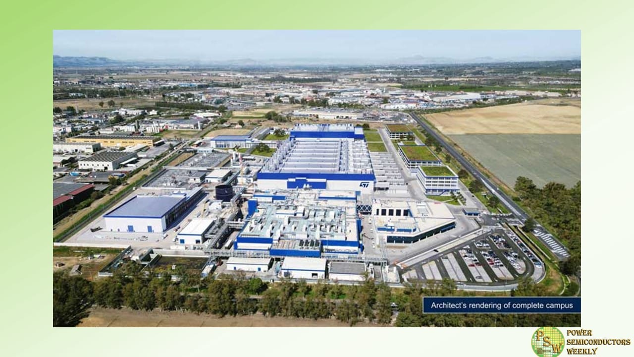
STMicroelectronics announced a new high-volume 200mm silicon carbide (“SiC”) manufacturing facility for power devices and modules, as well as test and packaging, to be built in Catania, Italy. Combined with the SiC substrate manufacturing facility being readied on the same site, these facilities will form ST’s Silicon Carbide Campus, realizing the Company’s vision of a fully vertically integrated manufacturing facility for the mass production of SiC on one site.
The creation of the new Silicon Carbide Campus is a key milestone to support customers for SiC devices across automotive, industrial and cloud infrastructure applications, as they transition to electrification and seek higher efficiency.
“The fully integrated capabilities unlocked by the Silicon Carbide Campus in Catania will contribute significantly to ST’s SiC technology leadership for automotive and industrial customers through the next decades,” said Jean-Marc Chery, President and Chief Executive Officer of STMicroelectronics. “The scale and synergies offered by this project will enable us to better innovate with high-volume manufacturing capacity, to the benefit of our European and global customers as they transition to electrification and seek more energy efficient solutions to meet their decarbonization goals.”
The Silicon Carbide Campus will serve as the center of ST’s global SiC ecosystem, integrating all steps in the production flow, including SiC substrate development, epitaxial growth processes, 200mm front-end wafer fabrication and module back-end assembly, as well as process R&D, product design, advanced R&D labs for dies, power systems and modules, and full packaging capabilities. This will achieve a first of a kind in Europe for the mass production of 200mm SiC wafers with each step of the process – substrate, epitaxy & front-end, and back-end – using 200 mm technologies for enhanced yields and performances.
The new facility is targeted to start production in 2026 and to ramp to full capacity by 2033, with up to 15,000 wafers per week at full build-out. The total investment is expected to be around five billion euros, with a support of around two billion euros provided by the State of Italy within the framework of the EU Chips Act. Sustainable practices are integral to the design, development, and operation of the Silicon Carbide Campus to ensure the responsible consumption of resources including water and power.
Original – STMicroelectronics
