Abstract
In this paper, a novel asymmetric trench SiC MOSFET with a Poly-Si/SiC heterojunction diode (HJD-ATMOS) is designed to improve its reverse conduction characteristics and switching performance. This structure features an integrated heterojunction diode, which improves body diode characteristics without affecting device static characteristics.
The heterojunction diode acts as a freewheeling diode during reverse conduction, reducing the cut-in voltage (Vcut-in) to a lower level than conventional asymmetric trench SiC MOSFET (C-ATMOS), while maintaining a similar breakdown voltage. Meanwhile, the split gate structure reduces gate-to-drain charge (Qgd). Through TCAD simulation, the HJD-ATMOS decreases Vcut-in by 53.04% compared to the C-ATMOS. Both Qgd and switching loss are reduced, with a decrease of 31.91% in Qgd and 40.29% in switching loss.
1. Introduction
The wide bandgap semiconductor properties of silicon carbide (SiC) make it a promising candidate for the development of future power switching devices. This is primarily due to SiC possessing properties such as a strong breakdown field, high physical and chemical stability, high thermal conductivity, and high electron saturation velocity.
SiC devices can operate in harsh environments due to their wide band gap of 3.25 eV and high thermal conductivity of 5 W/(cm·K). The SiC MOSFET is the most significant SiC power switching device due to its lack of trail current. This reduces switching loss and radiator volume, improving system power density.
SiC MOSFETs commonly make use of parasitic body-PN diodes as freewheeling diodes (FWD) in power inverter and converter systems. However, parasitic body-PN diodes in SiC MOSFETs are not ideal for use as freewheeling diodes. The reasons for this are as follows: Stacking faults (SFs) in SiC devices may cause reliability issues and increase conduction loss.
Although recent papers concerning the measured degradation of SiC MOSFETs show a high level of current threshold (about 5× the nominal current or more than 1000 A/cm2) for the starting of bipolar degradation, bipolar degradation effects can still occur in SiC MOSFETs under large cyclic pulse current densities. This will limit the application of SiC MOSFET devices in key areas, such as the surge current that flows through a diode during the start-up of a power converter, which can be more than ten times its rated current.
Furthermore, the body diode’s Vcut-in voltage (~2.7 V) is much higher than that of its silicon counterparts due to SiC’s wide bandgap. To overcome the drawbacks of parasitic body-PN diodes, numerous approaches have been devised to deactivate them. One approach is to integrate SiC MOSFETs with Schottky barrier diodes (SBDs). However, the use of external diodes not only introduces parasitic inductance, limiting switching frequency, but also consumes additional area in the package. And Schottky contacts suffer from a significant increase in reverse leakage current at high temperatures.
Furthermore, SiC MOSFETs with low-barrier and heterojunction diodes are available. Heterojunction diodes formed between polysilicon and SiC are attractive. Shenoy and Baliga, and Yamagami et al. presented studies on heterojunction diodes using P-Poly-Si and n-6H-SiC, and Poly-Si and 4H-SiC, respectively.
Both studies demonstrated low-forward-voltage Schottky-like characteristics. Ni et al. proposed a trench SiC MOSFET integrating polysilicon/SiC HJD, exhibiting excellent freewheeling diode (FWD) performance in both the first and third quadrants. The HJD’s unipolar behavior, similar to that of a Schottky diode, effectively suppresses the turn-on of the problematic body diode, mitigating the aging degradation observed in conventional SiC MOSFETs.
Additionally, HJDs reduce reverse recovery voltage and losses, enhancing long-term operational reliability. Furthermore, HJD integration eliminates the need for a separate SBD, leading to a smaller chip area, simpler packaging, and reduced overall system cost. This also minimizes parasitic inductance arising from additional components.
A novel asymmetric trench SiC MOSFET with a heterojunction diode at the right of the gate trench is proposed and simulated in this paper. The structure includes a trench gate with split-gate electrodes and a thicker P-Poly-Si layer, resulting in reduced gate charge and improved switching performance. To suppress the depletion layer, an n-type doped current spreading layer (N-CSL) is formed under the entire P-well region.
To maintain the breakdown voltage (BV) of the device structure while maintaining transfer and output characteristics similar to those of C-ATMOS, the depth of the P-well on the right side is not changed. The N-channel (Nch) is positioned below the P-Poly-Si and in contact with the CSL. The integrated HJD structure of the proposed device eliminates the requirement for an anti-parallel SiC SBD during reverse conduction. The HJD turns on at a low source–drain voltage (Vsd), thus eliminating bipolar degradation by inactivating the body diode. The split gate results in a decrease in gate charge, leading to a reduction in switching losses in the HJD-ATMOS without affecting other characteristics.
2. Device Structure and Mechanism
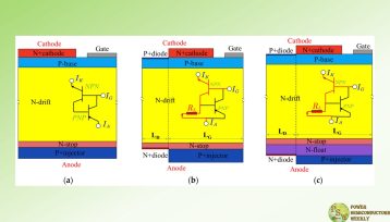
The schematic cross section of HJD-ATMOS and C-ATMOS is shown in Figure 1. Similar to C-ATMOS, the device forms an inversion layer channel in the first quadrant to facilitate electron conduction. The N-CSL layer on the N-drift region reduces the on-resistance. Deep P-wells are used to reduce the electric field stress in the gate oxide at the trench bottom and corner.
The primary distinction is the body diode structure. The Nch region under the P-Poly-Si provides a low-barrier path for electrons. Meanwhile, the HJD-ATMOS has a split gate and HJD structure on the right of the gate oxide layer. The split gate structure uses only a portion of the trench space for the gate electrode, while the other part is thicker P-Poly-Si that forms a portion of the HJD structure. The HJD-TMOS facilitates low-voltage conduction by allowing electrons to cross the lower heterojunction barrier in the third quadrant. The structure of Nch and N-channel doping concentration (Nnch) will be further discussed based on this optimization in this paper. Device specifications are presented in Table 1.
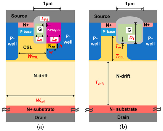
Figure 1. Schematic cross section of (a) HJD-ATMOS and (b) C-ATMOS.
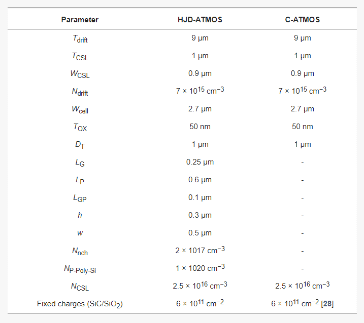
Table 1. Main parameters used in the simulation.
Sentaurus TCAD simulations are used to analyze the performances of the HJD-ATMOS and the C-ATMOS, considering doping and temperature-dependent Shockley–Read–Hall and Auger recombination, doping-dependent transport, impact ionization, band narrowing, high-field velocity saturation, and mobility degradation, as well as fixed charges at the SiC/SiO2 interface for closer simulation results to experimental data.
The energy band diagram of the P-Poly-Si/N-SiC heterojunction at thermal equilibrium is shown in Figure 2b. The energy band diagram at thermal equilibrium along the A-A’ cut-line is shown in Figure 2a. The heterojunction has a conduction energy gap of 0.46 eV and a valence barrier energy gap of 1.78 eV. The electron barrier height ΦBN is determined by the Fermi level energy Ef and the conduction band peak energy Ec, which is about 1.39 eV.
Figure 2c shows the simulated carrier density at the heterojunction interface under forward bias at the rated voltage. Electrons are injected from N-SiC to P-poly, but there are few holes from P-poly to N-SiC due to the high hole barrier. Therefore, the HJD exhibits unipolar action, similar to the SBD.
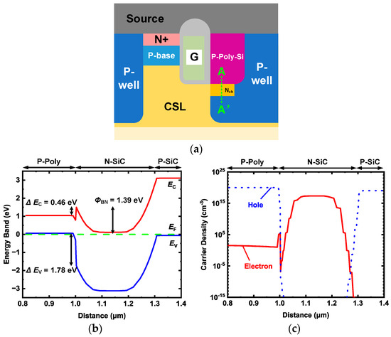
Figure 2. (a) Schematic cross section of HJD-ATMOS; (b) energy band diagram at thermal equilibrium along the A-A’ cut-line; (c) carrier density of the HJD when forward biased at rated voltage.
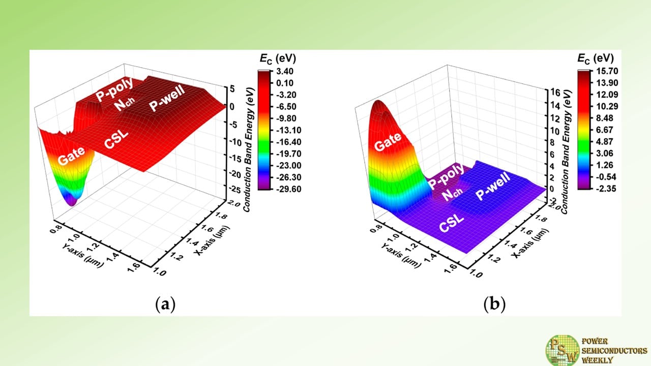
We also constructed a 3D band diagram of the device to better observe the working state of the device. Figure 3a shows the 3-D conduction band energy distribution of the device at Vds = 10 V and Vgs = 15 V. The band energy of Nch is higher than that of N-CSL, which prevents electron current from flowing to P-poly and enables the device to work normally like C-ATMOS.
Figure 3b shows the distribution of the devices when Vds = −5 V and Vgs = −5 V. The band energy of Nch is lower than that of N-CSL, resulting in electron current flowing from N-CSL to P-poly and preventing the turn-on of parasitic body-PN diodes.
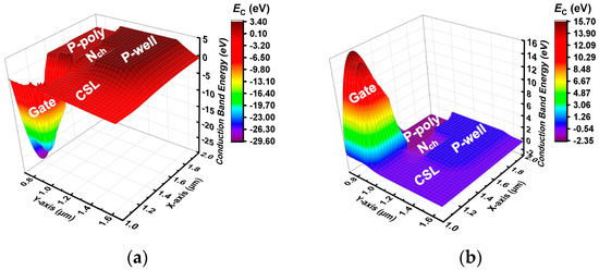
Figure 3. Three-dimensional conduction band energy distribution between P-poly, gate, Nch, N-CSL, and P-well (a) when conduction is forward and (b) when conduction is reverse.
Figure 4 shows the distribution of the total current density, hole current density, and electron current density of the device. From the total current density distribution, it can be seen that the current does not flow from P-Poly-Si to P-well. But a high current density is also noted at the gate corner of P-Poly-Si, which should be noted in use. From the hole current density distribution, it can be seen that holes do not enter N-drift.
This is due to the difference in the band gap between SiC and polysilicon. Since the energy barrier height between the SiC and polysilicon junctions in the valence band is very large, in the HJD-ATMOS, electron current can move toward the source while hole current cannot move toward the drain. The device can operate normally at electron current densities of 10 A/cm2 and 500 A/cm2.
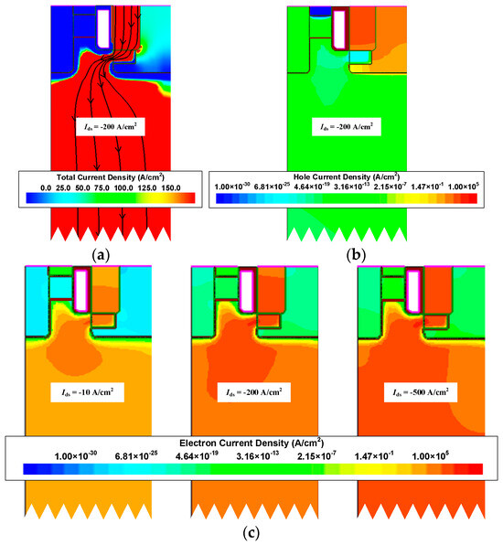
Figure 4. (a) Total current density distribution, (b) hole current density distribution, and (c) electron current density distribution at low and high current in the reverse conduction.
Figure 5 shows the I–V curves of HJD-ATMOS and C-ATMOS in forward and reverse conduction at room temperature. The steeper slope of the I–V curve of HJD-ATMOS in the first quadrant indicates that its specific on-resistance (Ron,sp) is lower than that of C-ATMOS. This is because the presence of Nch in HJD-ATMOS results in a smaller depletion region of P-well on N-CSL, leading to a wider current conduction region.
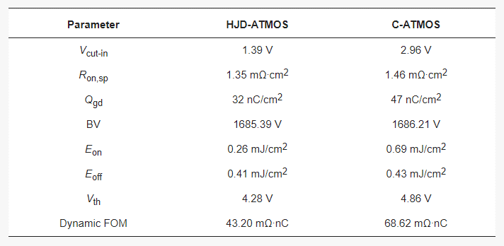
According to the calculations, at Vgs = 15 V and Ids = 200 A/cm2, the Ron,sp values for HJD-ATMOS and C-ATMOS are 1.35 mΩ∙cm2 and 1.46 mΩ∙cm2, respectively. In the third quadrant, at Ids= −10 A/cm2, HJD-TMOS exhibits a significantly lower Vcut-in of only 1.39 V compared to the PN diode of C-TMOS. As a result, HJD-ATMOS is capable of reducing switching losses.
The rated operating current of the device in the third quadrant is generally Ids = −200 A/cm2. This means that the proposed HJD-ATMOS has a clear advantage over C-ATMOS in that it can start working at a lower voltage. The hole density distribution diagram in Figure 5 for Ids = −200 A/cm2 shows that the integrated HJD effectively suppresses minority carrier injection, reducing bipolar degradation.
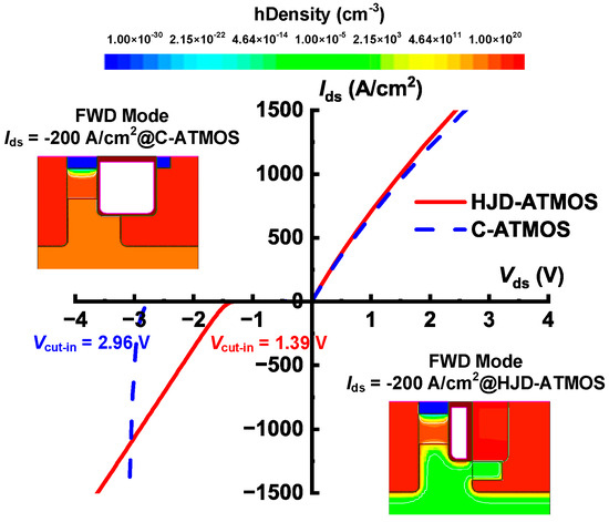
Figure 5. First and third quadrant characteristics of HJD-ATMOS and C-ATMOS.
In Figure 6, the local magnification shows that the HJD-ATMOS is affected by current spikes due to leakage. The figure demonstrates the change in breakdown voltage as a function of h and w when Nnch is, respectively, 2 × 1017 cm−3 and 2.5 × 1017 cm−3. It can be observed that when Nnch is 2.5 × 1017 cm−3, with h at 0.25 μm and w at 0.5 μm, the spike in the current is large, indicating the occurrence of leakage. When Nnch is 2.5 × 1017 cm−3, increasing h to 0.30 μm and w to 0.4 μm also results in leakage.
However, when Nnch is 2.0 × 1017 cm−3 and h increases to 0.3 μm, the device does not exhibit leakage, demonstrating that variations in Nnch have a significant impact on device performance. As shown in Figure 7, Vcut-in varies significantly with h. The minimum point of Vcut-in is 1.31 V at Nnch = 2 × 1017 cm−3, which is lower compared to its value of 1.71 V at Nnch = 2.5 × 1017 cm−3 and h = 0.2 μm.
This point represents the critical condition for the device not exhibiting leakage when Nnch = 2.5 × 1017 cm−3. After h is greater than 0.25 μm, the variation in Vcut-in with h tends to be flat, and if the value of h is larger, the protective effect of P-well on the gate oxide will also be weakened, and it will also increase the difficulty of process manufacturing.
As can be seen from Figure 8, when the device Vds is 0 V, Nnch is 2.5 × 1017 cm−3, and h is 0.25 μm, the HJD-ATMOS has more leakage than the device with Nnch is 2.0 × 1017 cm−3 and h is 0.30 μm. The darker regions in the current density plot for the HJD-ATMOS with Nnch at 2.5 × 1017 cm−3 and h at 0.25 μm are larger than those with Nnch at 2.0 × 1017 cm−3 and h at 0.30 μm, indicating higher leakage currents. This also confirms the hypothesis that the breakdown voltage spike is caused by heterojunction leakage. So the results indicate that Nnch = 2 × 1017 cm−3, h = 0.3 μm, and w = 0.5 μm are the optimal values.
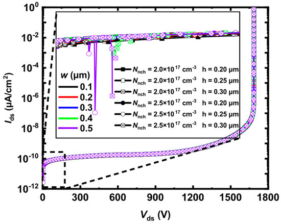
Figure 6. The breakdown voltage varies with h, w, and Nnch, when Nnch is 2.0 × 1017 cm−3 and 2.5 × 1017 cm−3, h is 0.20 μm, 0.25 μm and 0.30 μm, and w is 0.1 μm to 0.5 μm, respectively.
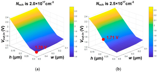
Figure 7. Vcut-in varies with h, w, and Nnch, when Nnch is (a) 2.0 × 1017 cm−3, and (b) 2.5 × 1017 cm−3.
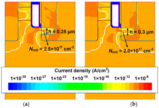
Figure 8. Current density distribution when (a) Nnch is 2.5 × 1017 cm−3, h is 0.25 μm, and (b) Nnch is 2.0 × 1017 cm−3, h is 0.30 μm at Vds = 0 V.
3. Simulation Results and Discussion
Figure 9 shows the capacitances of HJD-ATMOS and C-ATMOS. Gate voltage was fixed at 0 V, a 1 MHz AC signal was applied, and drain voltage was swept from 0 to 1000 V. HJD-ATMOS has lower gate-to-source capacitance (Cgs) than C-ATMOS due to the smaller contact area with the source caused by the split gate structure. HJD-ATMOS’s gate-to-drain capacitance (Cgd) does not decrease.
This is because the P-well blocks the right side of the gate of C-ATMOS, performing a similar function as the split gate. Therefore, it can be observed that the Ciss (Cgs + Cgd) of the HJD-ATMOS with split gates is also smaller than that of the C-ATMOS.
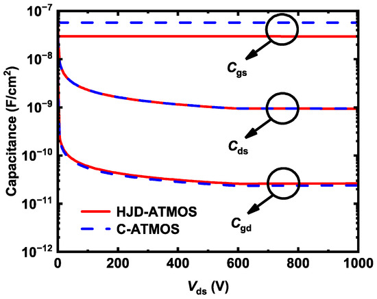
Figure 9. The device capacitance of HJD-ATMOS and C-ATMOS.
Gate-to-drain charge (Qgd) is critical for power device switching speed in device applications. Figure 10 shows a test circuit to simulate HJD-ATMOS and C-ATMOS gate charges during turn-on. The miller plateau height of HJD-ATMOS is less than that of C-ATMOS, indicating that the threshold voltage of HJD-ATMOS is smaller than that of C-ATMOS.
Because the gate charge is proportional to the gate capacitance, the HJD-ATMOS has a lower gate charge (Qg) and Qgd compared with the C-ATMOS. The Miller platform in HJD-ATMOS is shorter because of the reduced gate area. The Qgd values for HJD-ATMOS and C-ATMOS are 32 nC/cm2 and 47 nC/cm2, respectively. Qgd of HJD-ATMOS decreased by 31.91% compared to C-ATMOS. Reduced Qgd leads to a smaller high-frequency figure of merit in HJD-ATMOS.
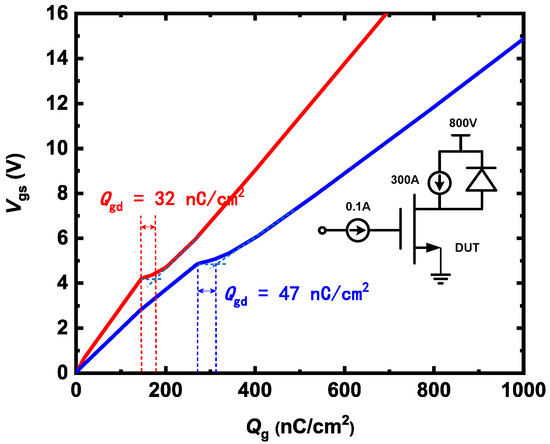
Figure 10. The gate charge characteristics of HJD-ATMOS and C-ATMOS.
Figure 11 shows the electric field distribution at the breakdown of HJD-ATMOS and C-ATMOS. The electric field at the gate oxide of HJD-ATMOS is smaller than that of C-ATMOS. This is because the presence of the Nch introduces a portion of the electric field into this region, which alleviates the electric field that the gate oxide withstands.
Although increasing the electric field at the heterojunction raises leakage current risk, it is a trade-off for improved reverse conduction performance. Figure 12 shows the blocking characteristics of the HJD-ATMOS and the C-ATMOS at room temperature and high temperature. At room temperature, the data are represented by solid lines, whereas at elevated temperatures, they are depicted by dashed lines. HJD-ATMOS and C-ATMOS have similar breakdown voltages at room temperature. But the leakage current of the HJD-ATMOS increases at high temperature due to the increased thermal energy of the charge carriers.
The generation of leakage currents, as demonstrated and discussed in Figure 6 and Figure 8, arises due to leakage occurring at the heterojunction, where higher Nnch and greater values of thickness h both contribute to this effect. By improving the semiconductor material growth process, reducing defects and traps, and enhancing the material quality and interface integrity, it is possible to mitigate non-ideal scattering and trap effects experienced by charge carriers at the heterojunction interface, thus suppressing the leakage current.
While the HJD-ATMOS structure does indeed experience leakage under temperature influence, this leakage is within acceptable limits, with the level of leakage current being 1 × 10⁻⁵ μA/cm2.
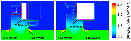
Figure 11. Electric field distribution for the HJD-ATMOS and the C-ATMOS at BV.
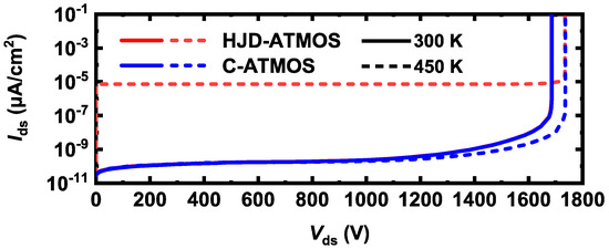
Figure 12. Blocking characteristics of the HJD-ATMOS and the C-ATMOS.
Figure 13 shows a double pulse test circuit for investigating switching characteristics. This is a common circuit configuration employed in device testing. Stray inductance is 10 nH, and load inductance is 80 μH. The gate voltage source (Vg) is turned on from −5 V to 15 V at t = 16 µs and turned off from 15 V to 0 V at t = 11 µs.
Figure 14 shows the switching waveforms of devices. The switching speed of the HJD-ATMOS is faster than that of the C-ATMOS with an external SBD diode, which results in a smaller switching loss. Figure 15 compares the switching losses between the two devices. In HJD-ATMOS, the turn-on loss (Eon) is 0.26 mJ/cm2, and the turn-off loss (Eoff) is 0.41 mJ/cm2, which demonstrate a reduction of 62.32% and 4.65%, respectively, compared to C-ATMOS.
The total switch loss of HJD-ATMOS is reduced by 40.29% compared to C-ATMOS. This is due to the smaller Qgd compared with the C-ATMOS. Reduced switching losses in power electronic devices are instrumental in improving operational longevity and reliability. As losses during switching are directly proportional to heat generation, a significant decrease in these losses curtails thermal build-up, mitigating the risk of device overheating and extending its operational life.
This reduction also sustains lower junction temperatures, crucial for preventing material degradation in high-power-density applications where maintaining low operating temperatures is vital for ensuring long-term stability and reliability. Furthermore, minimizing switching losses allows power converters and similar equipment to function efficiently at elevated frequencies without sacrificing efficiency, empowering designers to develop compact, lightweight systems while consistently meeting reliability standards.
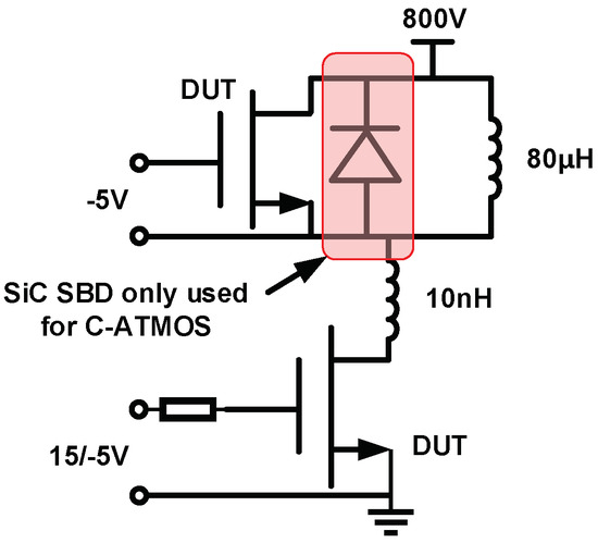
Figure 13. A circuit for simulating switching with a double pulsed test.
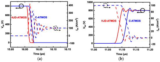
Figure 14. The switching characteristics of HJD-ATMOS and C-ATMOS, including the (a) turn-on process and (b) turn-off process.
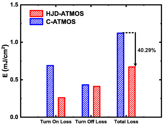
Figure 15. Switching loss comparison of IJ-ATMOS and C-ATMOS.
The majority of the process steps for HJD-ATMOS, including epitaxial growth, N+ source and P-well implantation, trench etching, P-base implantation, isolation oxidation, gate oxidation, polysilicon gate deposition, and metallization, are fully compatible with the manufacturing processes of C-ATMOS.
The N-channel region is formed by ion implantation at the bottom of the trench after trench etching. The split gate is formed by etching after trench oxidation, resulting in a thin layer of oxide between the gate and the P-Poly-Si. The gate-P-Poly-Si trench isolation layer is formed by thermal oxidation, and the trench oxide layer is fully etched and filled with P-Poly-Si.
Table 2 compares the HJD-ATMOS and the C-ATMOS in terms of their main characteristics. Dynamic FOM indicates the value of Ron,sp × Qgd. The HJD-ATMOS performs better due to the integrated HJD structure.
Table 2. Device characteristics comparison.
4. Conclusions
This paper proposes a novel asymmetric trench SiC MOSFET with a heterojunction diode. The performance of HJD-ATMOS and C-ATMOS is compared in detail. It can be observed that HJD-ATMOS demonstrates superior third-quadrant performance with a lower Vcut-in because of the integrated HJD. Compared with C-ATMOS, the Qgd of HJD-ATMOS has decreased by 31.91%. This is because the split gate design further reduces the total gate charge, which reduces the switching loss of the HJD-ATMOS device without affecting other key characteristics.
As a result, HJD-ATMOS eliminates bipolar degradation and reduces the turn-on loss from 0.69 mJ/cm2 in C-ATMOS to 0.26 mJ/cm2. With its advantageous features, HJD-ATMOS is a strong contender for power electronic applications.
Authors
Yiren Yu, Zijun Cheng, Yi Hu, Ruiyi Lv, Shengdong Hu.
Original – MDPI