
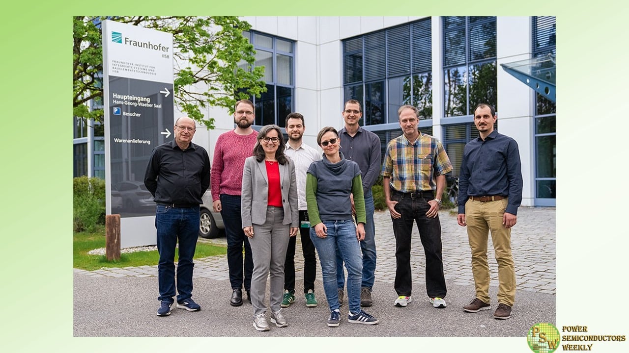
Semilab Zrt. and Fraunhofer IISB announced the official kick-off of their strategic partnership.
Within their new joint lab, located at the IISB in Erlangen, the partners develop state-of-the-art metrology and inspection solutions for (ultra-) wide-bandgap semiconductor materials.
The goal is to take semiconductor metrology to a next level along the value chain, from base material to die. By bringing new features and tools from lab to market, new standards for SiC, GaN and other (U)WBG semiconductors will be set.
Original – Fraunhofer IISB


