-

WeEn Semiconductors announced the launch of its 2000V High-Voltage (HV) series of standard rectifiers. Designed to address the evolving demands of high-voltage systems, these rectifiers achieve a 5% reduction in forward voltage drop (VF) and a 20% improvement in thermal resistance compared to competing solutions. The innovations enable significant efficiency gains, lower cooling costs and extended operational lifespans in renewable energy storage and electric vehicle (EV) fast-charging applications.
The 2000V HV series integrates a proprietary single-chip design to minimize conduction losses with an optimized ORing circuit that enhances thermal management. This combination ensures reliable performance in 1500V bus systems and 1000VDC EV charging infrastructure, where voltage spikes and stray inductance pose risks to component longevity. Additional advantages include:
- High Junction Temperature (Tjmax): Operates up to 150°C, ensuring stability in demanding environments.
- Superior Surge Current (IFSM) Tolerance: Enhances robustness under dynamic load conditions.
- TO247-2L Packaging: Streamlines integration into high-power designs.
Two initial variants are available: the 60A-rated WND60P20W and the 90A-rated WND90P20W. These devices are engineered to mitigate voltage spikes in fast-changing EV charging loads, safeguarding systems against failure while improving power density.
“The WND90P20W and WND60P20W resolve critical thermal and efficiency challenges in next-gen renewable energy and EV charging systems,” said Kevin Shen, President of WeEn Semiconductors. “By redefining voltage redundancy and thermal performance, we empower customers to deploy high-efficiency, low-maintenance solutions that outpace industry standards.”
The 2000V HV rectifiers are now available globally in TO247-2L packages. Target applications include solar PV inverter and storage systems, DC fast EV chargers, and industrial power systems requiring high voltage endurance and reliability.
Original – WeEn Semiconductors
-

Alpha and Omega Semiconductor Limited (AOS) announced its Mega IPM7 series intelligent power modules. Offering a highly efficient, compact, and durable design, this new series is optimized for brushless DC (BLDC) motor drive-based designs, including home appliance applications such as air-conditioners, refrigerators, dishwashers, and power tools.
The Mega IPM7 series is AOS’ new generation of intelligent power modules engineered to improve application performance and deliver increased power density all in a rugged, compact footprint that meets increasing space-constrained inverter design requirements. This energy-efficient power module also aids in enhancing the cost-effectiveness of fan motor applications. In addition, the advanced features of the Mega IPM7 series enable it to quickly and accurately detect module temperature, helping achieve highly reliable and long lifetime operation.
The Mega IPM7 series is offered in multiple packages, including the Mega IPM7-DT, the Mega7 DBC, and the Mega7 exposed package, allowing customers to select the package that best suits their heat dissipation performance specifications and other application-specific requirements.
“AOS is committed to staying ahead of our customers’ needs for increased power density and efficiency to help them meet market demands for greater performance, long lifetime, and rugged operation. The introduction of the Mega IPM7 series is specifically designed to boost the competitive advantages of BLDC-based applications. What’s more, AOS gives designers numerous package options to choose the one that ideally meets their performance needs,” said Dino Ge, Marketing Director of IGBT/IPM at AOS.
Technical Highlights
- 600V/1A – 600V/3A
- Compact package: 18mm x 7.5mm
- DBC technology
- 3-phase RC-IGBT inverter topology for motor drives
- Integrated HVIC gate driver including bootstrap circuit
- Integrated over-temperature protection and monitoring functions
Product Selection Table
Part Number Package Input Logic Rated Voltage (V) VCE(SAT) Typ. (V) AIM7DT3AR60V3 IPM-7DA Active High 600 1.5 AIM7E1AR60V1 IPM-7A Active High 600 2.0 AIM7ET1AR60V1 IPM-7B Active High 600 2.0 AIM7DT1AR60V3 IPM-7DA Active High 600 2.0 Original – Alpha and Omega Semiconductor
-

Fraunhofer IAF has developed a monolithic bidirectional switch with a blocking voltage of 1200 V using its GaN-on-insulator technology. The switch contains two free-wheeling diodes and can deliver performance and efficiency benefits in bidirectional chargers and drives for electric vehicles as well as in systems for generating and storing renewable energy. The results will be presented together with other developments in power electronics from May 6 to 8, 2025, at PCIM Europe in Nuremberg.
Technological innovations in power electronics are not only essential for the success of the energy transition, they also provide sustainable support for economic development in Europe. The Fraunhofer Institute for Applied Solid State Physics IAF develops power electronic components based on the wide-bandgap compound semiconductor gallium nitride (GaN) to enable further developments in electric mobility, the energy industry, and climate technology.
Most recently, Fraunhofer IAF has made significant progress in high-voltage and low-voltage components: At PCIM Europe 2025, researchers will present a highly integrated bidirectional switch (MBDS) with a blocking voltage of 1200 V. They will also demonstrate the use of a conventional GaN transistor with a gate contact as a bidirectional switch in a 3-level T-type converter. Both results were achieved as part of the GaN4EmoBiL project funded by the German Federal Ministry for Economic Affairs and Climate Action (BMWK).
“Geopolitical challenges such as the current tariff conflicts are an opportunity for European economies to gain technological advantages in the key areas of energy generation and mobility by developing their own solutions in power electronics,” emphasizes Achim Lösch, Business Developer for High Frequency and Power Electronics at Fraunhofer IAF.
“The added value of innovative power electronics is obvious: Achieving more power, better efficiency, and greater compactness at the same time advances the relevant technologies of the future: Electric cars charge faster and energy from renewable sources can be converted and stored more efficiently. At Fraunhofer IAF, we are working intensively to provide positive impetus in these important areas through innovative GaN-based components,” explains Lösch.
Researchers at Fraunhofer IAF have developed a GaN MBDS suitable for the 1200 V voltage class with integrated free-wheeling diodes and successfully integrated it into their own GaN technology. The researchers used the new GaN-on-insulator technology of Fraunhofer IAF for the manufacturing: Highly insulating materials such as silicon carbide (SiC) and sapphire are used as the carrier substrate for the GaN power semiconductor to improve the insulation between the components and increase the breakdown voltage.
The MBDS blocks voltage and conducts current in two directions, which saves chip space and reduces conduction losses as there is only one split depletion region. The GaN MBDS can be used in grid-connected power converters for energy generation and storage as well as electric drive systems. In these applications, the MBDS enables the development of systems in the 1200 V class.
Developers are working intensively on electric vehicles in this voltage class as increasing blocking voltages offer significant advantages in terms of everyday usability: Charging power increases and energy losses during operation decrease as a result of lower resistance. Electric cars with 400 V currently dominate the market, but 800 V technology is gaining ground. The leap to 1200 V has a positive effect on the long-distance capability of electric cars and the utility value of electric trucks.
The 1200 V GaN MBDS with integrated peripherals will be presented by Dr. Michael Basler at the PCIM Conference on May 8 from 10:10 to 10:30 a.m. in the oral session on GaN Devices II on Stage München 1. It is based on Basler’s paper “Highly-Integrated 1200 V GaN-Based Monolithic Bidirectional Switch,” which will be published in conjunction with PCIM 2025.
Fraunhofer IAF has also made progress in the field of multi-level converters with bidirectional switches for blocking voltages up to 48 V: Researchers have used a conventional single-gate HEMT (high electron mobility transistor) based on the aluminum gallium nitride/gallium nitride (AlGaN/GaN) compound semiconductor heterostructure in a low-voltage 3-level T-type converter as a bidirectional switch, thereby achieving simpler control of the transistor than with a bidirectional transistor with two gates for such topologies. Like the 1200 V MBDS, this innovative approach enables simpler control in addition to a space-efficient component design.
On May 6, Daniel Grieshaber will present the results shown in his paper “Investigation of a Single-Gate GaN HEMT as Bidirectional Switch in a Low Voltage Multilevel Topology” at the PCIM Conference Poster Session in the GaN Devices I section from 3:30 to 5:00 p.m. in the foyer.
In addition to innovations in the field of bidirectional switches, researchers at Fraunhofer IAF are working along the entire semiconductor value chain on materials, components, modules and subsystems for GaN-based power electronics in the voltage classes 48 V, 100 V, 200 V, 600 V and 1200 V. The current focus is on lateral and vertical components, monolithic integration, and highly insulating substrates such as sapphire or SiC. In addition to the results presented at PCIM 2025, Fraunhofer IAF is already working on components in the 1700 V class.
Fraunhofer IAF will be presenting an overview of its research and development portfolio in power electronics at the PCIM Expo in Hall 6, Booth 260, from May 6 to 8. Among others, an epitaxial 8-inch GaN wafer, processed 4-inch GaN-on-SiC and GaN-on-sapphire wafers, GaN power ICs, integrated lateral and vertical GaN components and 600 V half-bridge modules based on GaN are being exhibited.
At the PCIM Conference, Dr. Richard Reiner will also summarize the latest power electronics developments at Fraunhofer IAF in his presentation “Lateral, Vertical, Bidirectional! Innovations and Progress in GaN Devices and Power ICs.” It will take place on May 7 from 10:50 to 11:10 a.m. on the Technology Stage.
Original – Fraunhofer IAF
-

ROHM has developed the new 4-in-1 and 6-in-1 SiC molded modules in the HSDIP20 package optimized for PFC and LLC converters in onboard chargers (OBC) for xEVs (electric vehicles). The lineup includes six models rated at 750V (BSTxxx1P4K01) and seven products rated at 1200V (BSTxxx2P4K01). All basic circuits required for power conversion in various high-power applications are integrated into a compact module package, reducing the design workload for manufacturers and enabling the miniaturization of power conversion circuits in OBCs and other applications.
In recent years, the rapid electrification of cars is driving efforts to achieve a decarbonized society. Electric vehicles are seeing higher battery voltages to extend the cruising range and improve charging speed, creating a demand for higher output from OBCs and DC-DC converters. At the same time, there is an increasing need in the market for greater miniaturization and lighter weight for these applications, requiring technological breakthroughs to improve power density – a key factor – while enhancing heat dissipation characteristics that could otherwise hinder progress.
ROHM’s HSDIP20 package addresses these technical challenges that were previously becoming difficult to overcome with discrete configurations, contributing to both higher output and the downsizing of electric powertrains.
The HSDIP20 features an insulating substrate with excellent heat dissipation properties that suppresses the chip temperature rise even during high power operation. When comparing a typical OBC PFC circuit utilizing six discrete SiC MOSFETs with top-side heat dissipation to ROHM’s 6-in-1 module under the same conditions, the HSDIP20 package was verified to be approx. 38°C cooler (at 25W operation).
This high heat dissipation performance supports high currents even in a compact package, achieving industry-leading power density more than three times higher than top-side cooled discretes and over 1.4 times that of similar DIP type modules. As a result, in the PFC circuit mentioned above, the HSDIP20 can reduce mounting area by approx. 52% compared to top-side cooled discrete configurations, greatly contributing to the miniaturization of power conversion circuits in applications such as OBCs.
Going forward, ROHM will continue to advance the development of SiC modules that balance miniaturization with high efficiency while also focusing on the development of automotive SiC IPMs that provide higher reliability in a smaller form factor.
Original – ROHM
-

SemiQ Inc has announced a family of co-packaged 1200 V SOT-227 MOSFET modules based on its third-generation SiC technology.
In addition to smaller die sizes, third generation SIC devices offer faster switching speeds and reduced losses.
The family of highly rugged and easy mount devices currently offers six devices with an RDSon range of 8.4 to 39 mΩ: GCMS008C120S1-E1, GCMX008C120S1-E1, GCMS016C120S1-E1, GCMX016C120S1-E1, GCMS040C120S1-E1 and GCMX040C120S1-E1, with the GCMX040C120S1-E1 having a switching time as low as 67 ns. In addition to these six, two further modules – GCMS080C120S1-E1 and GCMX080C120S1-E1 – are available, each with an RDSon of 80 mΩ.
The COPACK MOSFETs with Schottky barrier diode provides exceptional switching losses at high junction temperature due to the low turn on switching losses.
SemiQ is targeting the robust SiC MOSFET modules at applications including solar inverters, energy storage systems, battery charging, and server power supplies. All devices have been screened with wafer-level gate-oxide burn-in tests and tested beyond 1400 V, with avalanche testing to 330 mJ (RDSon = 39 mΩ) or 800 mJ (RDSon = 16.5 or 8.4 mΩ).
In addition to having a drain-to-source voltage (VDS) of 1200 V, the MOSFET reduces total switching losses to as low as 468 µJ and a reverse recovery charge of 172 nC (GCMX040C120S1-E1). The family also has a low junction-to-case thermal resistance and comes with an isolated backplate and the ability to directly mount to a heatsink by 4kVAC galvanic isolation testing.
Specifications: Ratings and electrical/thermal characteristics
The QSiC 1200 V MOSFET modules have a continuous operational and storage temperature of -55oC to 175oC. It has a recommended operational gate-source voltage of -4.5/18 V, with a VGSmax of -8/22 V, and a power dissipation of 183 to 536 W (RDSon = 39 and mΩ, core and junction temperature 25oC).
For static electrical characteristics, the device has a junction-to-case thermal resistance of 0.23oC per watt (RDSon = 8.4) as well as a typical zero-gate voltage drain current of 100 nA, and a gate-source voltage current of 10 nA.
The fastest switching device has a turn-on delay time of 13 ns with a rise time of 7 ns; its turn-off delay time is 18 ns with a fall time of 29 ns.
Original – SemiQ
-
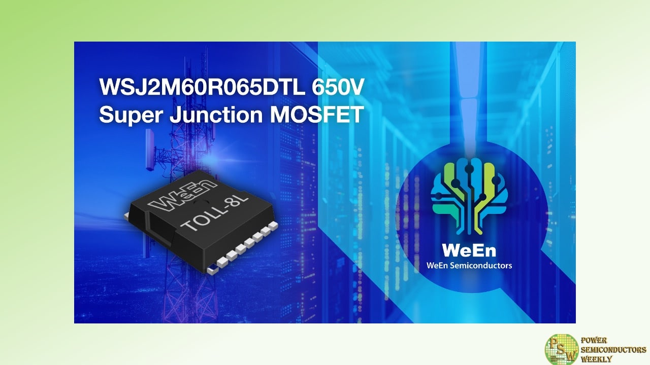
WeEn Semiconductors will exhibit the company’s latest 600 V super junction MOSFET for computing and telecoms server applications at this year’s PCIM Expo conference and trade fair. The WSJ2M60R065DTL has been specifically developed to address the demands of artificial intelligence (AI) and other high-performance processing applications by enabling improved efficiency, smaller form factors and easier thermal management.
Based on the company’s latest generation super junction technology, the WeEn WSJ2M60R065DTL super junction MOSFET combines an industry-leading on resistance (RDS(ON)) and figure of merit (RDS(ON)*Qg) with an ultra-compact TOLL package. Visitors to PCIM in Nuremberg from 6th – 8th May 2025 will have the opportunity to see this advanced technology on the WeEn booth (Hall 9, booth 131), alongside other bipolar products including silicon-controlled rectifiers, power diodes, high voltage transistors and silicon carbide (SiC) devices.
The WSJ2M60R065DTL is rated for 50 A, features a maximum RDS(ON) of 65 mΩ and has a typical blocking voltage of around 700 V. An integrated and fine-tuned forward recovery diode (FRD) ensures excellent reverse recovery robustness and balanced high-temperature performance. The body diode can withstand a commutation speed of 1000 A/μs without damage, making the WSJ2M60R065DTL particularly suitable for Zero Voltage Switching (ZVS) applications in soft-switching topologies where it can deliver high efficiency while handling irregular operating conditions. At the same time, stable resistance performance delivers a steady and predictable RDS(ON) across a range of current and temperature conditions.
In developing the new MOSFET, WeEn has focused on precise control of the charge balance of the super junction structure. This ensures robust avalanche ruggedness and low capacitive losses that allow for an optimized balance of RDS(ON) and EOSS As with all WeEn technologies, reliability is a prime consideration and the company conducts extensive and reliability checks. All of the company’s super junction MOSFETs demonstrate not only consistency among samples but good ESD capabilities and zero aging during reliability examinations.
Original – WeEn Semiconductors
-

Littelfuse, Inc. announced the release of the IXD2012NTR, a high-speed, high-side and low-side gate driver designed to drive two N-channel MOSFETs or IGBTs in a half-bridge configuration. The IXD2012NTR is optimized for high-frequency power applications, delivering superior switching performance and enhanced design flexibility.
The IXD2012NTR operates over a wide 10 V to 20 V voltage range and supports a high side switch of up to 200 V in a bootstrap operation. Its logic inputs are compatible with standard TTL and CMOS levels down to 3.3 V, ensuring seamless integration with a wide range of control devices. With a 1.9 A source and 2.3 A sink output capability, the IXD2012NTR provides robust gate drive currents ideal for high-speed switching applications.
The device’s integrated cross-conduction protection logic prevents the high- and low-side outputs from turning on simultaneously, while simplifying circuit design through a high level of integration. Offered in a compact SOIC(N)-8 package and operational over a temperature range of −40 °C to +125 °C, the IXD2012NTR delivers reliable performance even in harsh environments.
Key Features and Benefits
- High-Speed Switching Performance: Drives two N-channel MOSFETs or IGBTs in a half-bridge configuration.
- Wide Operating Voltage Range: 10 V to 20 V for versatile power management applications.
- High Side Switching Capability: Operates up to 200 V in a bootstrap configuration.
- Compatibility and Flexibility: Logic inputs compatible with TTL and CMOS levels down to 3.3 V for easy interfacing with controllers.
- Output Current Drive Capability: 1.9 A source and 2.3 A sink output for robust gate drive currents.
- Enhanced Efficiency and Integration: Integrated cross-conduction protection reduces power loss and simplifies design.
- Industry-Standard Pinout: Ensures drop-in replacement capability for existing designs.
“The IXD2012NTR is a direct drop-in replacement to popular, industry-standard gate driver devices,” said June Zhang, Product Manager, Integrated Circuits Division of Littelfuse Semiconductor Business Unit. “This addition to our portfolio provides customers with a reliable, alternate source to meet demanding production schedules while delivering exceptional high-speed performance.”
Ideal for Diverse Markets and Applications
The IXD2012NTR enhances the Littelfuse portfolio of high- and low-side gate drivers by offering a new 200 V device. It supports various high-frequency applications, including:
- DC-DC converters
- AC-DC inverters
- Motor controllers
- Class-D power amplifiers
The IXD2012NTR is well-suited for use in several markets:
- General industrial and electrical equipment
- Appliances
- Building solutions
- Energy storage
- Solar energy
- Power tools
Original – Littelfuse
-

The JANS qualification represents the highest level of screening and acceptance requirements, ensuring the superior performance, quality and reliability of discrete semiconductors for aerospace, defense and spaceflight applications. Microchip Technology announced its completion of its family of radiation-hardened (rad-hard) power MOSFETs to the MIL-PRF-19500/746 slash-sheet specification and the achievement of JANSF qualification for its JANSF2N7587U3, 100V N-channel MOSFET to 300 Krad (Si) Total Ionizing Dose (TID).
Microchip’s JANS series of rad-hard power devices is available in voltage ranges from 100–250V to 100 Krad (Si) TID, with the family expanding to higher Radiation Hardness Assurance (RHA) levels, starting with the JANSF2N7587U3 at 300 Krad (Si) TID. The JANS RH MOSFET die is available in multiple package options including a plastic package using the MIL-qualified JANSR die, providing a cost-effective power device for New Space and Low Earth Orbit (LEO) applications. The ceramic package is hermetically sealed and developed for total dose and Single-Event-Environments (SEE).
The devices are designed to meet the MIL-PRF19500/746 standard with enhanced performance, making them excellent options for applications that demand high-reliability components capable of withstanding the harsh environments of space and extending the reliability of power circuitry.
“Meeting the stringent specifications required for rad-hard MOSFETs is extremely challenging, and Microchip is pleased to achieve this development milestone by leveraging its proprietary rad-hard by design process and technology,” said Leon Gross, corporate vice president of Microchip’s discrete products group. “Our advanced technology provides our aerospace and defense customers with highly reliable and cost-effective solutions that meet the growing demand of the market and their applications.”
The JANSF and JANSR RH power MOSFETs serve as the primary switching elements in power conversion circuits, including point-of-load converters, DC-DC converters, motor drives and controls, and general-purpose switching. With low RDS(ON) and a low total gate charge, these power MOSFETs offer improved energy efficiency, reduced heat generation and enhanced switching performance when compared to similar devices on the market.
Original – Microchip Technology
-

Navitas Semiconductor announced the release of its latest SiCPAK™ power modules with epoxy-resin potting technology, powered by proprietary trench-assisted planar SiC MOSFET technology, that have been rigorously designed and validated for the most demanding high-power environments, prioritizing reliability and high-temperature performance. Target markets include EV DC fast chargers (DCFC), industrial motor drives, interruptible power supplies (UPS), solar inverters and power optimizers, energy storage systems (ESS), industrial welding, and induction heating.
The new portfolio of 1200V SiCPAK™ power modules, enabled by advanced epoxy-resin potting technology, are engineered to withstand high-humidity environments by preventing moisture ingression and enable stable thermal performance by reducing degradation from power and temperature variations.
Navitas’ SiCPAK™ modules demonstrated 5x lower thermal resistance increase following 1000 cycles of thermal shock testing (-40 C to + 125 C) compared to conventional silicone-gel-filled case-type modules. Furthermore, all silicone-gel-filled modules failed isolation tests while SiCPAK™ epoxy-resin potted modules maintained acceptable isolation levels.
Enabled by over 20 years of SiC innovation leadership, Navitas’ GeneSiC™ ‘trench-assisted planar SiC MOSFET technology’ provides industry-leading performance over temperature, enabling up to 20% lower losses, cooler operation, and superior robustness to support long-term system reliability.
The ‘trench-assisted planar’ technology enables an extremely low RDS(ON) increase versus temperature, which results in the lowest power losses across a wider operating range and offers up to 20% lower RDS(ON) under in-circuit operation at high temperatures compared to competition. Additionally, all GeneSiC™ SiC MOSFETs have the highest-published 100%-tested avalanche capability, up to 30% better short-circuit withstand energy, and tight threshold voltage distributions for easy paralleling.
The 1200V SiCPAK™ power modules have built-in NTC thermistors and are available from 4.6 mΩ to 18.5 mΩ ratings in half-bridge, full-bridge, and 3L-T-NPC circuit configurations. They are pin-to-pin compatible with industry-standard press-fit modules. Additionally, optional pre-applied Thermal Interface Material (TIM) for simplified assembly is available.
Original – Navitas Semiconductor
-

The market for electric vehicles continues to gather pace with a strong volume growth of both battery electric vehicles (BEVs) and plug-in hybrid electric vehicles (PHEVs). The share of electric vehicles produced is expected to see double-digit growth by 2030 with a share of around 45 percent compared to 20 percent in 2024. Infineon Technologies AG is responding to the growing demand for high-voltage automotive IGBT chips by launching a new generation of products. Among these offerings are the EDT3 (Electric Drive Train, 3 rd generation) chips, designed for 400 V and 800 V systems, and the RC-IGBT chips, tailored specifically for 800 V systems. These devices enhance the performance of electric drivetrain systems, making them particularly suitable for automotive applications.
The EDT3 and RC-IGBT bare dies have been engineered to deliver high-quality and reliable performance, empowering customers to create custom power modules. The new generation EDT3 represents a significant advancement over the EDT2, achieving up to 20 percent lower total losses at high loads while maintaining efficiency at low loads. This achievement is due to optimizations that minimize chip losses and increase the maximum junction temperature, balancing high-load performance and low-load efficiency. As a result, electric vehicles using EDT3 chips achieve an extended range and reduce energy consumption, providing a more sustainable and cost-effective driving experience.
“Infineon, as a leading provider of IGBT technology, is committed to delivering outstanding performance and reliability”, says Robert Hermann, Vice President for Automotive High Voltage Chips and Discretes at Infineon Technologies. “Leveraging our steadfast dedication to innovation and decarbonization, our EDT3 solution enables our customers to attain ideal results in their applications.”
The EDT3 chipsets, which are available in 750 V and 1200 V classes, deliver high output current, making them well-suited for main inverter applications in a diverse range of electric vehicles, including battery electric vehicles, plug-in hybrid electric vehicles, and range-extended electric vehicles (REEVs). Their reduced chip size and optimized design facilitate the creation of smaller modules, consequently leading to lower overall system costs. Moreover, with a maximum virtual junction temperature of 185°C and a maximum collector-emitter voltage rating of up to 750 V and 1200 V, these devices are well-suited for high-performance applications, enabling automakers to design more efficient and reliable powertrains that can help extend driving range and reduce emissions.
“Infineon, as Leadrive’s primary IGBT chip supplier and partner, consistently provides us with innovative solutions that deliver system-level benefits,” said Dr. Ing. Jie Shen, Founder and General Manager of Leadrive. “The latest EDT3 chips have optimized losses and loss distribution, support higher operating temperatures, and offer multiple metallization options. These features not only reduce the silicon area per ampere, but also accelerate the adoption of advanced packaging technologies.”
The 1200 V RC-IGBT elevates performance by integrating IGBT and diode functions on a single die, delivering an even higher current density compared to separate IGBT and diode chipset solutions. This advancement translates into a system cost benefit, attributed to the increased current density, scalable chip size, and reduced assembly effort.
Infineon’s latest EDT3 IGBT chip technology is now integrated into the HybridPACK™ Drive G2 automotive power module, delivering enhanced performance and capabilities across the module portfolio. This module offers a power range of up to 250 kW within the 750 V and 1200 V classes, enhanced ease of use, and new features such as an integration option for next-generation phase current sensors and on-chip temperature sensing, contributing to system cost improvements.
All chip devices are offered with customized chip layouts, including on-chip temperature and current sensors. Additionally, metallization options for sintering, soldering and bonding are available on request.
The new EDT3 and RC-IGBT devices are already available for sampling. Further information is available at www.infineon.com/edt3
Original – Infineon Technologies
