-
Data centers are currently responsible for more than two percent of global energy consumption. Fueled by AI, this number is expected to grow to up to around seven percent in 2030, matching the current energy consumption of India. Enabling efficient power conversion from grid-to-core is vital to enable superior power densities and thereby advance compute performance while reducing total cost of ownership (TCO).
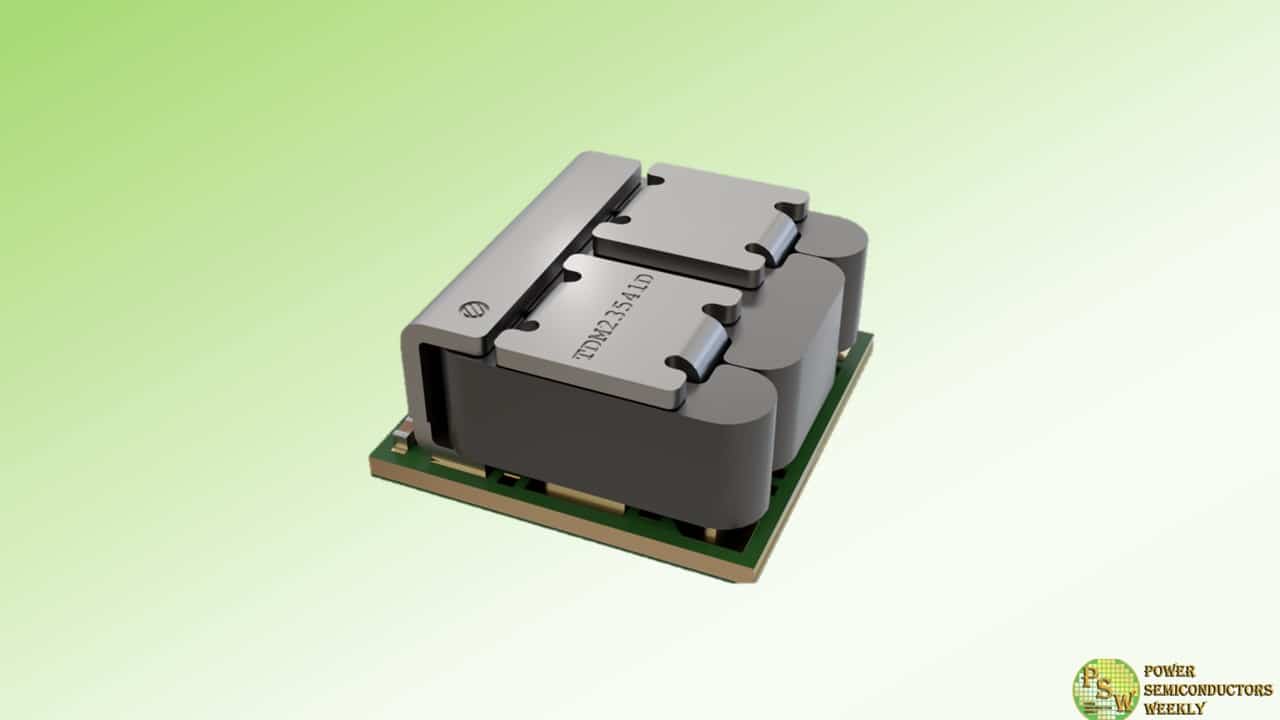
Infineon Technologies AG is therefore launching the TDM2354xD and TDM2354xT dual-phase power modules with best-in-class power density for high-performance AI data centers. These modules enable true vertical power delivery (VPD) and offer industry’s best current density of 1.6 A/mm2. They follow the TDM2254xD dual-phase power modules introduced by Infineon earlier this year.
“We are proud to enable high-performance AI data centers with our TDM2354xT and TDM2354xD VPD modules. These devices will maximize system performance with Infineon’s trademark quality and robustness, thereby enabling best TCO for data centers,” said Rakesh Renganathan, Vice President Power ICs at Infineon Technologies. “Our industry-leading power devices and packaging technologies, combined with our extensive systems expertise, will further advance high-performance and green computing as part of our mission to drive digitalization and decarbonization.”
The TDM2354xD and TDM2354xT modules combine Infineon’s robust OptiMOS™ 6 trench technology, a chip-embedded package that enables superior power density through enhanced electrical and thermal efficiencies, and a new inductor technology to enable lower profile and therefore, true vertical power delivery.
As a result, the modules set new standards in power density and quality to maximize the compute performance and efficiency of AI data centers. The TDM2354xT modules support up to 160 A and are the industry’s first Trans-Inductor Voltage Regulator (TLVR) modules in a small 8 x 8 mm² form factor. Combined with Infineon’s XDP™ controllers, they offer extremely fast transient response and minimize on-board output capacitance by up to 50 percent, further increasing system power density.
The new modules will be showcased at Infineon’s global technology forum OktoberTech™ 2024 in Silicon Valley on 17 October and at electronica 2024 in Munich from November 12 to 14 (hall C3, booth 502).
Original – Infineon Technologies
-

Navitas Semiconductor announced that its high-power GaNSafe family is now available in a TOLT (Transistor Outline Leaded Top-side cooling) package.
The GaNSafe family has been specifically created to serve demanding, high-power applications, such as AI data centers, solar/energy storage, and industrial markets. Navitas 4th generation integrates control, drive, sensing, and critical protection features that enable unprecedented reliability and robustness. GaNSafe is the world’s safest GaN with short-circuit protection (350ns max latency), 2kV ESD protection on all pins, elimination of negative gate drive, and programmable slew rate control. All these features are controlled with 4-pins, allowing the package to be treated like a discrete GaN FET, requiring no VCC pin.
The TOLT packaging enhances thermal dissipation through the top side of the package, allowing heat to be dissipated directly to the heatsink (not through the PCBA). This enables the reduction of operating temperature and increases current capability, resulting in the highest level of system power density, efficiency, and reliability.
“With over 200 million units shipped and supplied with a 20-year warranty, Navitas’ highly integrated high-power GaNSafe ICs are proven to deliver performance and reliability while simplifying Design-IN for systems up to 22kW,” says Charles Bailley, Senior Director of Business Development. “As the most protected, reliable, and safe GaN devices in the industry, GaNSafe took our technology into mainstream applications above 1kW. Now, with the enhanced thermal dissipation of the TOLT package, we are enabling customers to deliver even better performance, efficiency, power density, and reliability in even the most demanding applications.”
Suitable for applications from 1 kW to 22 kW, 650 V GaNSafe in TOLT packaging is available with a range of RDS(ON)MAX from 25 to 98 mΩ. Integrated features and functions include:
- High-speed short-circuit protection, with autonomous ‘detect and protect’ with ultra-fast 350 ns / 50 ns latency.
- Protected, regulated, integrated gate-drive control, with zero gate-source loop inductance for reliable high-speed 2 MHz switching capability to maximize application power density.
- Electrostatic discharge (ESD) protection of 2 kV, compared to zero for discrete GaN transistors.
- 650 V continuous, and 800 V transient voltage capability for extraordinary application conditions.
- Integrated Miller Clamp (no negative gate bias, higher 3rd quadrant efficiency)
- Programmable turn-on and turn-off speeds (dV/dt) to simplify EMI regulatory requirements.
- Simple 4-pin device, allowing the package to be treated like a discrete GaN and requiring no additional VCC pin
- Robust, thermally enhanced packaging: ultra-low RQ_JUNC-AMB and board-level thermal cycling (BLTC) Reliability
In addition to the new ICs, Navitas will be offering reference design platforms based on GaNSafe TOLT for applications including data center power supplies and EV on-board chargers. These system platforms include complete design collateral with fully tested hardware, embedded software, schematics, bill-of-materials, layout, simulation, and hardware test results.
Original – Navitas Semiconductor
-
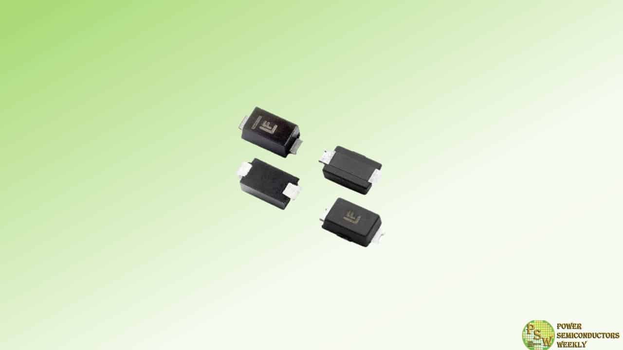
Littelfuse, Inc. announced the SMFA Asymmetrical Series Surface-Mount TVS Diode, the first-to-market asymmetrical TVS solution specifically designed to protect Silicon Carbide (SiC) MOSFET gates from overvoltage events. As SiC MOSFETs become increasingly popular due to their faster switching speeds and superior efficiency compared to traditional Silicon MOSFETs and IGBTs, the need for robust gate protection has never been greater. The SMFA Asymmetrical Series offers an innovative, single-component solution that significantly enhances circuit reliability while simplifying design.
The SMFA Asymmetrical Series is the only TVS diode on the market engineered specifically for the unique gate protection requirements of SiC MOSFETs. Unlike traditional solutions that require multiple Zener or TVS diodes, the SMFA Series effectively protects against ringing and overshoot phenomena in gate drive circuits using a single component, saving valuable PCB space and reducing the complexity of circuit designs.
The SMFA Asymmetrical Series Surface-Mount TVS Diode offers the following key features and benefits:
- Asymmetrical Design: The SMFA Series is tailored to the specific negative and positive gate voltage ratings of SiC MOSFETs, ensuring precise and reliable protection.
- Single-Component Solution: Replaces multiple Zener and TVS diodes, reducing the number of components and simplifying circuit layout.
- Space Efficiency: By combining multiple protection functions into one component, the SMFA Series minimizes PCB space usage, allowing for more compact and efficient designs.
- Compatibility: The SMFA Asymmetrical Series is compatible with all available Littelfuse and other leading SiC MOSFETs, making it a versatile solution for various applications.
“The SMFA Asymmetric TVS Diodes protect valuable SiC MOSFETs from gate failures using a single component solution that easily replaces multiple Zener and TVS diodes,” said Ben Huang, Director of Product Marketing at Littelfuse. “This unique solution also saves valuable PCB space while reducing the number of components required.”
The SMFA Asymmetrical Series is ideal for a variety of demanding applications where SiC MOSFETs are used, including:
- AI / Data Center Server Power Supplies: Enhances the reliability and efficiency of critical power supplies in high-performance computing environments.
- High-Efficiency Electric Vehicle Infrastructure (EVI) Power Systems: Provides robust gate protection in EV charging stations and related power systems, ensuring longevity and performance.
- High-Reliability Semiconductor/Industrial Equipment Power Supplies: Protects essential power supplies in industrial and semiconductor manufacturing environments, where reliability and uptime are paramount.
Original – Littelfuse
-
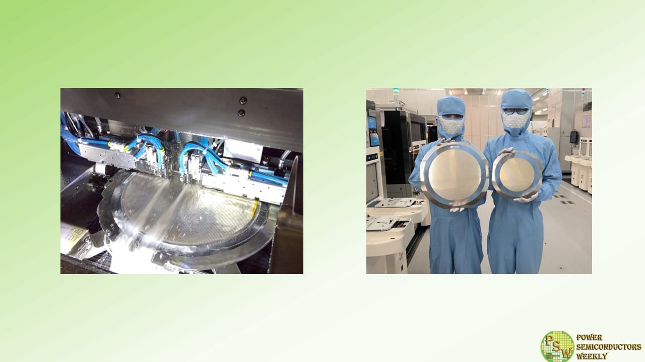
Mitsubishi Electric Corporation announced that its Power Device Works’ Fukuyama Factory has begun large-scale supply of power semiconductor chips made from 12-inch silicon (Si) wafers for the assembly of semiconductor modules.
The advanced Si power-semiconductor modules will initially be used in consumer products. Going forward, Mitsubishi Electric expects to contribute to green transformation (GX) by providing a stable and timely supply of semiconductor chips to meet the growing demand for energy-saving power-electronics devices in various applications.
The Fukuyama Factory processes wafers for the production of Si power-semiconductors. The factory is playing a key role in Mitsubishi Electric’s medium-term plan to double its wafer processing capacity for Si power- semiconductors by fiscal 2026 compared to five years earlier. By supplying large quantities of 12-inch Si wafers for power semiconductor chips, the company will ensure stable production of advanced Si power-semiconductor modules for energy-saving power-electronics equipment.
Original – Mitsubishi Electric
-
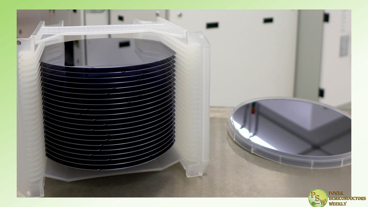
Coherent Corp. announced the launch of its 200 mm silicon carbide epitaxial wafers. Substrate and epi-wafer shipments from the company at 350 micron and 500 micron thickness are now underway.
As a dedicated manufacturer of both SiC substrates and epitaxial wafers, Coherent combines these elements to deliver exceptional quality, performance, and reliability. The new 200 mm SiC epi-wafers are engineered with cutting-edge thickness and doping uniformity, setting new industry standards and supporting the production of superior SiC power semiconductors.
“With our advanced technology, we are not only enhancing the quality of SiC devices but also addressing the growing demand for 200 mm for efficient power-conversion components in critical sectors,” said Gary Ruland, Vice President and General Manager of the SiC Materials Business Unit.
SiC devices are integral to power conversion in electric and hybrid vehicles, energy infrastructure, and high-power EV chargers. The transition from 150 mm to 200 mm diameter wafers responds to the increasing demand for SiC semiconductors, allowing manufacturers to produce more devices per wafer. This shift is expected to enhance productivity and reduce the cost of SiC devices, benefiting a wide range of applications.
By adopting larger wafers, SiC device manufacturers can achieve higher yields and improved cost efficiency because of a 1.8x increase in usable area per wafer. The implementation of state-of-the-art 200 mm tooling brings additional advantages while aligning with the industry’s drive for greater performance and reduced operational costs.
Original – Coherent
-
 LATEST NEWS / PRODUCT & TECHNOLOGY / SiC / WBG
Axus Technology Introduced Industry’s Lowest Cost of Ownership for CMP Processes on 200mm SiC Wafers
September 26, 2024
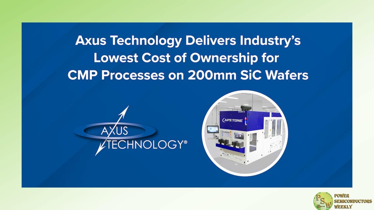
2 Min ReadAxus Technology, a leading global provider of chemical mechanical planarization (CMP) equipment, critical for semiconductor and compound semiconductor fabrication, announced its flagship CapstoneÆ CS200 platform tools offer the industry’s lowest cost of ownership (CoO) for CMP processes on 200mm silicon carbide (SiC) wafers. Compared to its closest competitor, Axus’s small-footprint Capstone delivers twice the throughput at less than half the total cost per wafer.
Yole Group forecasts the overall SiC manufacturing tool market to top US$4.4 billion by 2029. “The unique properties of SiC require specialized manufacturing tools and lines for processing power SiC devices,” the market analyst firm noted earlier this year. Axus anticipated this need, designing the state-of-the-art Capstone from the ground up to deliver advanced processing capabilities for SiC in power electronics and other applications.
“Many 200mm fabs are looking to upgrade their installed base of CMP tools to products with leading-edge capability and functionality. Our ability to deliver industry-low CoO further underscores our strong market position and capacity to support this shift,” said Axus Technology CEO Dan Trojan. “Capstone features a streamlined workflow and integrated cleaning capability, so it requires half the process steps of older CMP tools. This allows customers to greatly lower their capex investment.”
Key Capstone CoO advantages vs. competitor
- Throughput: 2.5x wafers per hour
- Power consumption: 60% lower
- DI water consumption: 80% lower
- Footprint: 45% smaller
- Capex cost per wafer: 65% lower
- Total cost per wafer: 50% lower
Another factor contributing to Capstone’s lower CoO is its built-in Process Temperature Control (PTC) technology, which enables processing at higher pressures and speeds without exceeding temperature limits of polishing pads and other sensitive components. This feature is vital for SiC and other materials with high hardness and planarization challenges that necessitate more aggressive process conditions.
Axus built its proprietary CoO model using its own system specifications, publicly available specs for competitive tools, actual consumables costs, and real-world performance data supplied by customers. The comprehensive model factors in all CoO contributors: process variables (polish time and removal rates), polishing and cleaning consumables, power and deionized (DI) water usage, system footprint, and equipment capex including cost, utilization and wafer capacity.
Original – Axus Technology
-
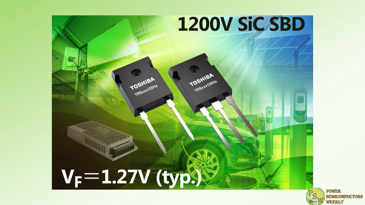
Toshiba Electronics Europe GmbH enhances its silicon carbide (SiC) diode portfolio with ten new 1200V Schottky barrier diodes (SBDs). The TRSxxx120Hx series, comprising five products housed in TO-247-2L packages and five in TO-247 packages, helps designers improve the efficiency of industrial equipment, including photovoltaic (PV) inverters, electric vehicle (EV) charging stations, and switching power supplies.
By implementing an enhanced junction barrier Schottky (JBS) structure, the TRSxxx120Hx series allows a very low forward voltage (VF) of just 1.27V (typ.). The merged PiN-Schottky incorporated into a JBS structure reduces diode losses under high current conditions. The TRS40N120H of the new series accepts a forward DC current (IF(DC)) of 40A (max) and a non-repetitive peak forward surge current (IFSM) of 270A (max), with the maximum case temperature (TC) of all devices being +175°C.
Combined with the lower capacitive charge and leakage current, the products help improve system efficiency and simplify thermal design. For instance, at a reverse voltage (VR) of 1200V, the TRS20H120H diode housed in the TO-247-2L package provides a total capacitive charge (QC) of 109nC and reverse current (IR) of 2µA.
Original – Toshiba
-
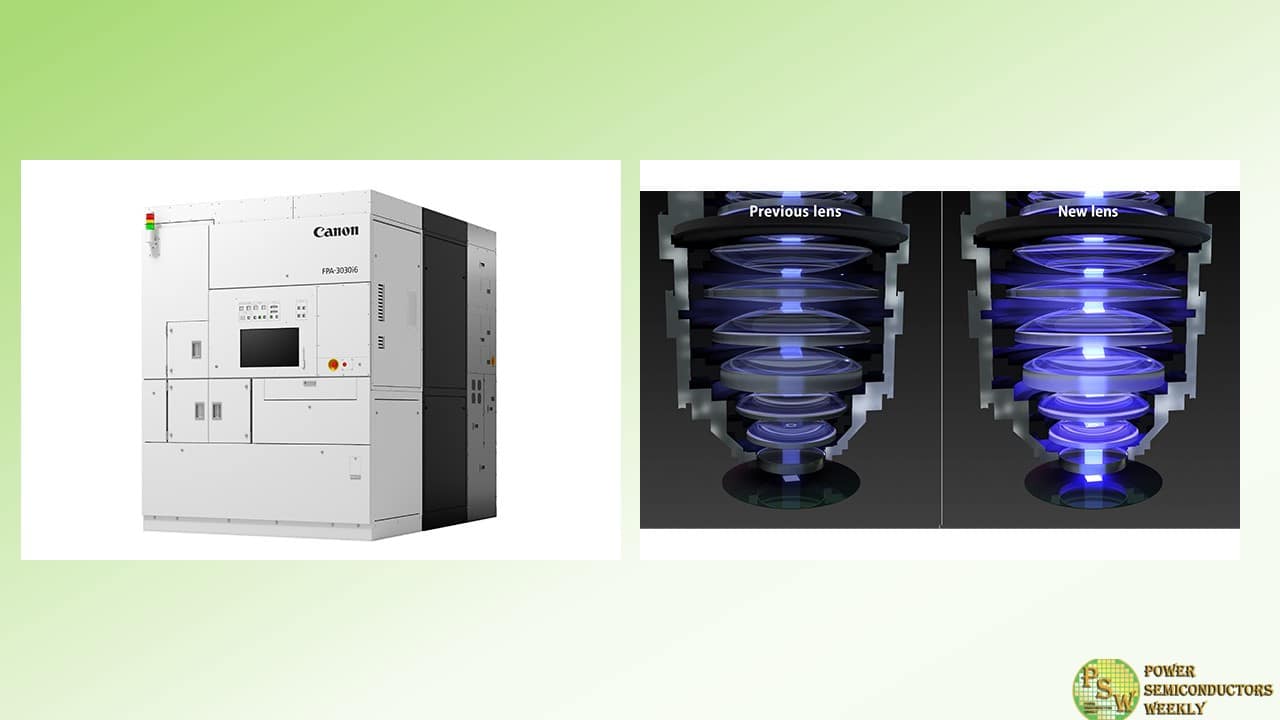
Canon Inc. announced the release of the FPA-3030i6 i-line stepper, a new semiconductor lithography system for processing wafers with a diameter of 8 inches (200 mm) or smaller.
The FPA-3030i6 employs a newly developed projection lens that boasts high transmittance and high-durability. The system reduces lens aberration for high exposure dose processes and improves productivity by shortening exposure time.
The lens is made of high-transmittance glass material that reduces lens aberrations occurring during exposure by more than 50% when compared to previous stepper models. Higher transmittance also helps reduce exposure time while maintaining pattern fidelity, even under high exposure dose conditions.
Improving lens transmittance will also increase exposure intensity and shorten the exposure time required for each process. The FPA-3030i6 standard productivity for 8 inch (200 mm) wafers has increased to 130 wafers per hour from 123 for the previous stepper models.
Additionally, since the lens is highly durable, lens transmittance decrease over time is reduced and productivity can be maintained over the life of the system.
The NA (numerical aperture) range has also been expanded from 0.45~0.63 in the previous model to 0.30~0.63. Allowing for a smaller NA enables customers to select the optimum NA for each device layer.
Optional products including a wafer handling system for special substrates are available for order to meet users’ manufacturing needs for various emerging semiconductor devices including high-power and high-efficiency green devices.
The FPA-3030i6 is designed to support a wider range of device fabrication thanks to a variety of available process options for silicon (Si) as well as sapphire and compound semiconductor materials such as silicon carbide (SiC), gallium nitride (GaN) and gallium arsenide (GaAs) substrates.
Canon will offer wafer feeding options enabling handling of substrates from 2 inches (50 mm) to 8 inches (200 mm) in diameter, as well as thick, thin and warped substrate handling.
Original – Canon
-
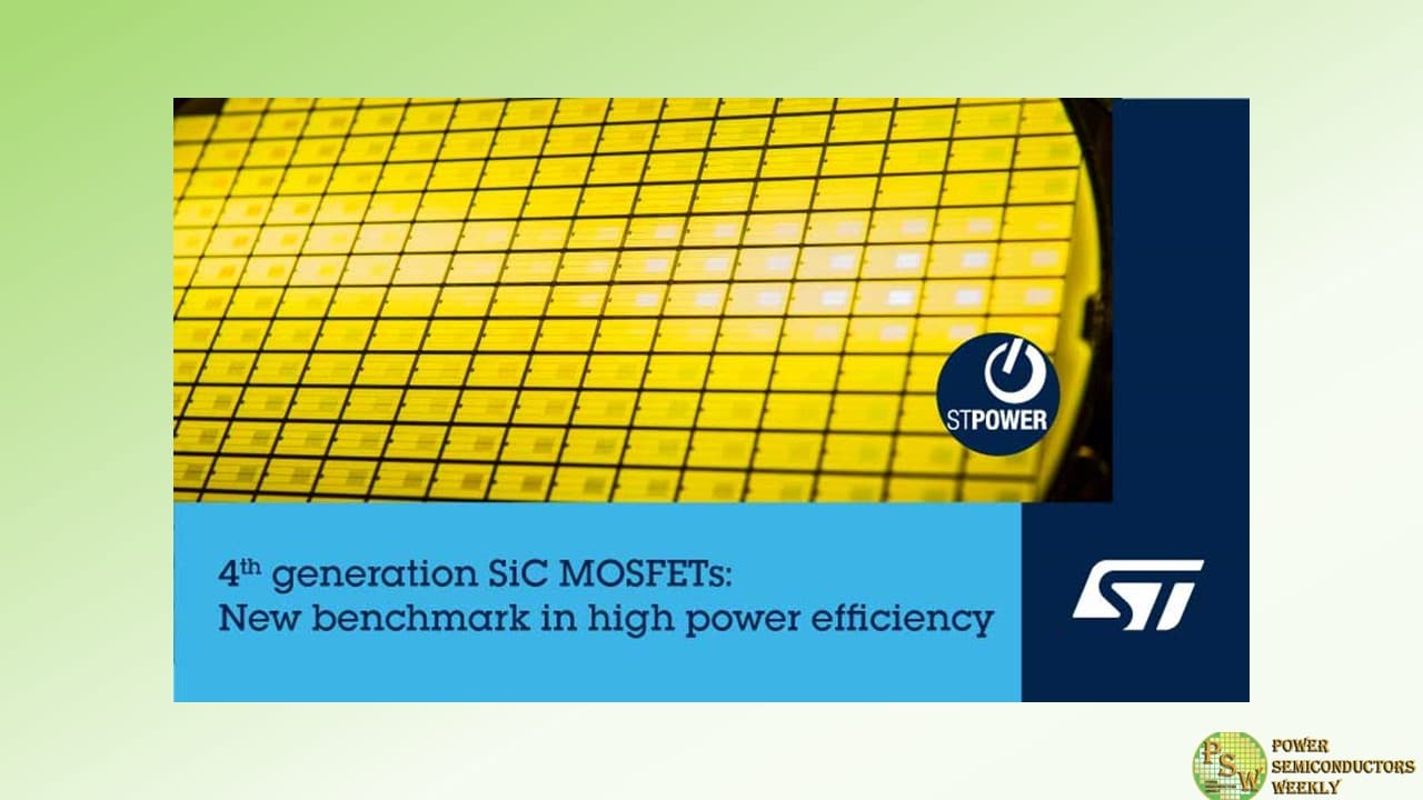
STMicroelectronics introduced its fourth generation STPOWER silicon carbide (SiC) MOSFET technology. The Generation 4 technology brings new benchmarks in power efficiency, power density and robustness. While serving the needs of both the automotive and industrial markets, the new technology is particularly optimized for traction inverters, the key component of electric vehicle (EV) powertrains. The company plans to introduce further advanced SiC technology innovations through 2027 as a commitment to innovation.
“STMicroelectronics is committed to driving the future of electric mobility and industrial efficiency through our cutting-edge silicon carbide technology. We continue to advance SiC MOSFET technology with innovations in the device, advanced packages, and power modules,” said Marco Cassis, President, Analog, Power & Discrete, MEMS and Sensors Group. “Together with our vertically integrated manufacturing strategy, we are delivering industry leading SiC technology performance and a resilient supply chain to meet the growing needs of our customers and contribute to a more sustainable future.”
As the market leader in SiC power MOSFETs, ST is driving further innovation to exploit SiC’s higher efficiency and greater power density compared to silicon devices. This latest generation of SiC devices is conceived to benefit future EV traction inverter platforms, with further advances in size and energy-saving potential. While the EV market continues to grow, challenges remain to achieve widespread adoption and car makers are looking to deliver more affordable electric cars.
800V EV bus drive systems based on SiC have enabled faster charging and reduced EV weight, allowing car makers to produce vehicles with longer driving ranges for premium models. ST’s new SiC MOSFET devices, which will be made available in 750V and 1200V classes, will improve energy efficiency and performance of both 400V and 800V EV bus traction inverters, bringing the advantages of SiC to mid-size and compact EVs — key segments to help achieve mass market adoption.
The new generation SiC technology is also suitable for a variety of high-power industrial applications, including solar inverters, energy storage solutions and datacenters, significantly improving energy efficiency for these growing applications.
ST has completed qualification of the 750V class of the fourth generation SiC technology platform and expects to complete qualification of the 1200V class in the first quarter of 2025. Commercial availability of devices with nominal voltage ratings of 750V and 1200V will follow, allowing designers to address applications operating from standard AC-line voltages up to high-voltage EV batteries and chargers.
ST’s Generation 4 SiC MOSFETs provide higher efficiency, smaller components, reduced weight, and extended driving range compared to silicon-based solutions. These benefits are critical for achieving widespread adoption of EVs and leading EV manufacturers are engaged with ST to introduce the Generation 4 SiC technology into their vehicles, enhancing performance and energy efficiency. While the primary application is EV traction inverters, ST’s Generation 4 SiC MOSFETs are also suitable for use in high-power industrial motor drives, benefiting from the devices’ improved switching performance and robustness.
This results in more efficient and reliable motor control, reducing energy consumption and operational costs in industrial settings. In renewable energy applications, the Generation 4 SiC MOSFETs enhance the efficiency of solar inverters and energy storage systems, contributing to more sustainable and cost-effective energy solutions. Additionally, these SiC MOSFETs can be utilized in power supply units for server datacenters for AI, where their high efficiency and compact size are crucial for the significant power demands and thermal management challenges.
To accelerate the development of SiC power devices through its vertically integrated manufacturing strategy, ST is developing multiple SiC technology innovations in parallel to advance power device technologies over the next three years. The fifth generation of ST SiC power devices will feature an innovative high-power density technology based on planar structure. ST is at the same time developing a radical innovation that promises outstanding on-resistance RDS(on) value at high temperatures and further RDS(on) reduction, compared to existing SiC technologies.
ST will attend ICSCRM 2024, the annual scientific and industry conference exploring the newest achievements in SiC and other wide bandgap semiconductors. The event, from September 29 to October 04, 2024, in Raleigh, North Carolina will include ST technical presentations and an industrial keynote on ‘High volume industrial environment for leading edge technologies in SiC’.
Original – STMicroelectronics
-
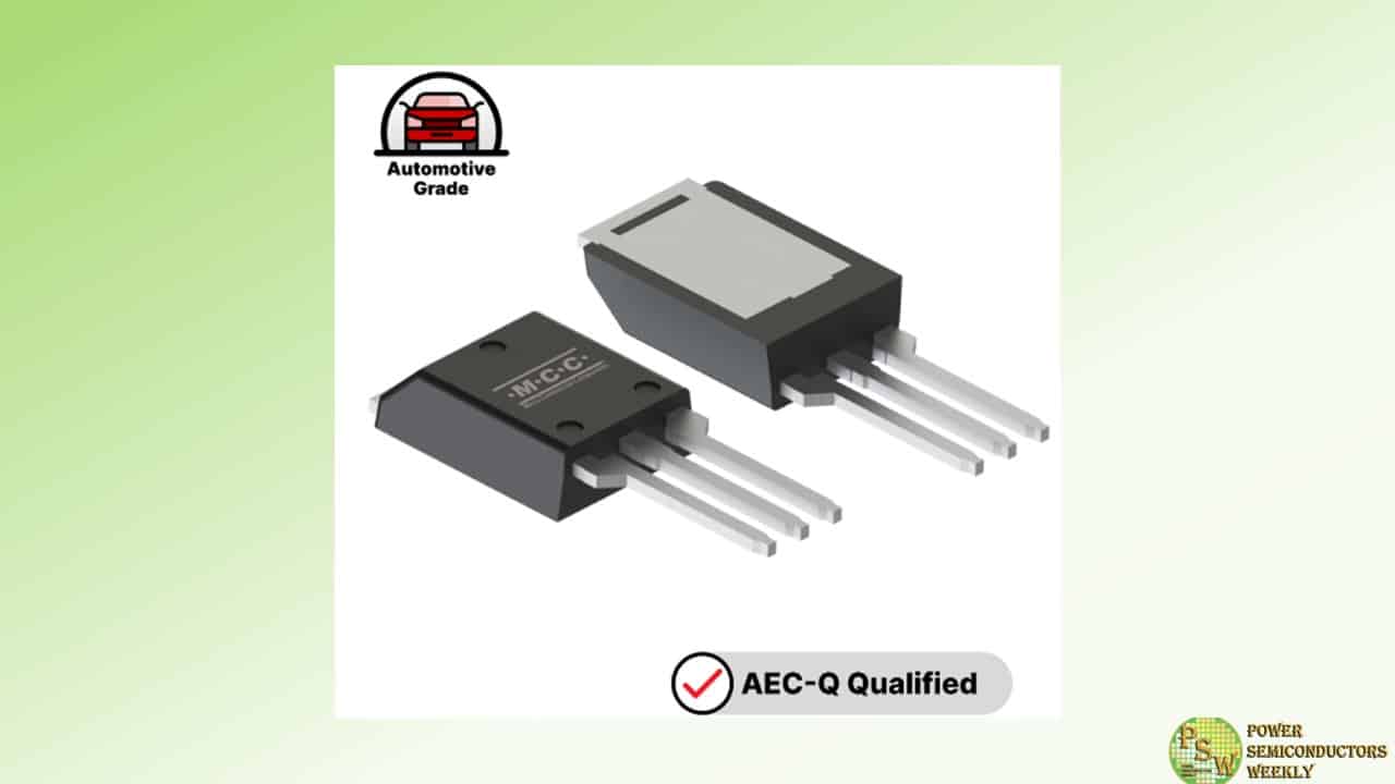
MCC released 1200V Auto-Grade Trench Field-Stop IGBT engineered for demanding automotive applications. MIS80N120NT1YHE3 delivers reliable switching where other components fall short, minimizing losses while maintaining thermal performance.
Its super TO-220 package design boasts a junction-to-case thermal resistance of only 0.17K/W for maximum heat dissipation in high-voltage scenarios. But the superior thermal performance doesn’t stop there. With a low saturated VCE of just 2.25V and operating junction temperature of up to 150°C, this IGBT enhances energy efficiency and boosts overall performance.
Advanced trench field-stop technology provides an additional layer of optimized switching efficiency, adding to its reliability. Rigorously tested to achieve AEC-Q101 qualification, this IGBT is equipped with the robustness required in extreme automotive environments.
From PTC heaters and solid-state relays and electric drive systems, MCC’s new 1200V IGBT is the obvious solution for engineers looking to improve system integrity and efficiency in diverse applications.
Features & Benefits:
- AEC-Q101 Qualified: Meets stringent automotive quality standards for enhanced reliability.
- 1200V High Breakdown Voltage: Capable of handling high-voltage operations, making it ideal for automotive applications.
- Low Saturated VCE: Achieves 2.25V (typ.) at higher temperatures, minimizing energy loss and enhancing efficiency.
- Low Switching Losses: Enable efficient operation, contributing to improved overall system performance.
- Excellent Thermal Performance: Housed in a super TO-220 package (TO-273AA) with a junction-to-case thermal resistance of 0.17K/W, ensuring effective heat dissipation.
- High Thermal Stability: Maintains performance across a wide temperature range for unwavering operation in varying scenarios.
- Powerful Short-Circuit Protection: Integrated features safeguard against damage in fault conditions, enhancing safety and dependability.
- Versatile Application Compatibility: Suitable for a wide range of automotive applications, including PTC heaters, solid-state relays, electric drive systems, renewable energy systems, and industrial motor drives.
Original – Micro Commercial Components
