-

Infineon Technologies AG has been a pioneer in the market introduction of silicon carbide (SiC) power devices and trench technology for SiC MOSFETs, combining excellent performance with high robustness. Today, the CoolSiC™ product offering spans from 400 V to 3.3 kV and covers a broad range of applications, including automotive drivetrains, EV charging, solar energy systems, energy storage, and high-power traction inverters.
Building on a solid track record in SiC business development and leveraging its position as the innovator of charge-compensating devices in silicon (CoolMOS™), Infineon is now introducing a trench-based SiC superjunction (TSJ) technology concept.
“With the introduction of the TSJ concept, we are significantly expanding the technological capabilities of silicon carbide,” said Peter Wawer, President of Infineon’s Green Industrial Power Division. “The combination of trench and superjunction technology enables higher efficiency and more compact designs – an important step for applications requiring the highest levels of performance and reliability.”
Infineon is committed to gradually expanding its CoolSiC product portfolio, leveraging SiC TSJ technology. This expansion will encompass a diverse range of package types, including discretes, molded and frame-based modules, as well as bare dies. The extended portfolio will cater to a broad spectrum of applications, targeting both the automotive and industrial sectors.
The first products based on the new technology will be 1200 V in Infineon ID-PAK for automotive traction inverters and combine the advantages of trench technology and superjunction design, capitalizing on Infineon’s more than 25 years of experience in SiC and silicon-based superjunction technology (CoolMOS). This scalable package platform supports power levels of up to 800 kW, enabling a high degree of system flexibility. Key benefits of the technology include increased power density, achieved through an up to 40 percent improvement in R DS(on)*A, allowing for more compact designs within a given power class. Additionally, the 1200 V SiC trench-superjunction concept in ID-PAK enables up to 25 percent higher current capability in main inverters without compromising short-circuit capability.
This advancement also results in enhanced overall system performance, delivering improved energy efficiency, reduced cooling requirements, and higher reliability for demanding automotive and industrial applications. Moreover, the system benefits from reduced parallelization requirements, which simplify the design process and lower overall system costs. With these innovations, the Infineon ID-PAK package equipped with SiC TSJ technology contributes to the development of more efficient and cost-effective traction inverter designs for automotive applications.
“As the global number one in automotive semiconductors, Infineon sets the pace of innovation and helps build the bridge between technological progress of vehicles and sustainable mobility,” said Peter Schiefer, President of Infineon’s Automotive Division. “Our new trench-based SiC superjunction technology brings further value to electric vehicle drivetrains enabling higher efficiency and system design simplicity.”
As an early customer, Hyundai Motor Company development teams will engage with Infineon’s trench-superjunction technology, leveraging its benefits to enhance their EV offerings. This partnership is expected to drive the development of more efficient and compact EV drivetrains.
Initial ID-PAK 1200 V samples are now available for selected automotive drivetrain customers. The SiC TSJ-based ID-PAK 1200 V package is expected to be ready for volume production in 2027.
Original – Infineon Technologies
-

Cambridge GaN Devices (CGD) announced that Inventchip, a leading provider of SiC power devices and IC solutions headquartered in Shanghai, has successfully demo’d a 2.5 kW GaN-based CCM totem-pole PFC reference design using CGD’s ICeGaN® gallium nitride ICs. A key feature is ease-of use. ICeGaN ICs integrate interface circuitry and protection on the same GaN die as the HEMT. Therefore, any standard driver IC can be used. The Inventchip IVCC1104 totem pole PFC controller IC is also simple to use with no programming required. It offers optimized AC zero-crossing control, low THD and high robustness against AC disturbance.
DI CHEN | DIRECTOR, TECHNICAL MARKETING AND BUSINESS DEVELOPMENT, CGD
“Inventchip had an existing 2.5kW TPPFC reference design based on its controller and gate drivers using SiC MOSFETs in TO-247 packages. To evaluate the performance of GaN instead, Inventchip designed a TO-247 adapter board using our P2 25mΩ ICeGaN ICs and the ICeGaN design works perfectly without any modification of their circuits. It has demonstrated that the ICeGaN can significantly shorten the learning curve and allow engineers to bring new product faster to market.”DR. ZHONG YE |CTO , INVENTCHIP
“By using a TO247-4 adapter board to solder on a DFN-packaged ICeGaN device for a quick test on our EVM, despite the relatively long gate drive path and the extended drive power supply trace, the board was powered up successfully at the first shot with clean switching waveform. No abnormalities or shoot-through was observed from no-load to full-load conditions. The GaN’s performance is very impressive. The CGD GaN device has proven to be very noise-immune, user-friendly and highly efficient.”Having proved its efficiency and power density in low power charger designs, GaN is now being adopted by makers of server and data centre PSUs, inverters, industrial brick DC/DC converters and LED drivers. Soon, EV inverter drives of over 100 kW are expected to transition to GaN too. ICeGaN technology is especially suitable at higher power levels because of its proven reliability and robustness.
Original – Cambridge GaN Devices
-

Power Integrations announced five new reference designs targeting 800 V automotive applications based on the company’s 1700 V InnoSwitch™3-AQ flyback switcher ICs. Spanning power levels from 16 W to 120 W, the designs leverage both wound and low-profile planar transformers and target automotive applications such as DC-DC bus conversion, inverter emergency power, battery management and power supplies for auxiliary systems. The designs feature Power Integrations’ new wide-creepage InSOP™-28G package, which supports 1000 VDC on the primary side while providing appropriate creepage and clearance between pins in pollution degree 2 environments.
“The new InSOP™-28G package, with its wide 5.1 mm drain-to-source pin creepage distance, addresses the critical need for enhanced safety and reliability in high-voltage applications,” said Mike Stroka, product marketing engineer at Power Integrations. “It provides sufficient isolation that conformal coating can be eliminated, saving a manufacturing process step and associated qualification effort. The InnoSwitch3-AQ IC, featuring a 1700 V silicon-carbide (SiC) switch, is an ideal solution for 800 V vehicles, simplifying manufacturing while enhancing overall system performance and reliability.”
Available from www.power.com, the following reference designs are all isolated flyback converters based on the 1700 V-rated CV/CC InnoSwitch3-AQ switcher ICs. The three reference designs kits (RDKs) and two design example reports (DERs) are:
- RDK-994Q— 35 W ultra-low-profile traction inverter gate-drive or emergency power supply with 40-1000 VDC input and 24 V output;
- RDK-1039Q— 18 W power supply with planar transformer for traction inverter gate driver or emergency power supply;
- RDK-1054Q— 120 W power supply with planar transformer, designed to shrink or eliminate heavy, bulky 12 V batteries;
- DER-1030Q— 20 W four-output power supply—one emergency power supply (EPS) with 24.75 V output and three gate-drive power supplies with 25.5 V output;
- DER-1045Q— 16 W four-output power supply—one 14 V EPS output and three gate-drive outputs with split +18 V / -5 V rails.
Power Integrations’ 1700 V-rated SiC-based CV/CC InnoSwitch3-AQ switching power supply ICs deliver up to 120 watts of output power. The highly integrated ICs reduce power supply bill of materials (BOM) count by as much as 50 percent, saving space, enhancing system reliability and easing component sourcing challenges. Devices start up with as little as 30 volts on the drain pin without external circuitry, which is often a critical requirement for functional safety.
Additional protection features include input under-voltage, output over-voltage and over-current limiting. Power consumption is less than 15 mW at no-load. The ICs also incorporate synchronous rectification and a valley switching, discontinuous/continuous conduction mode (DCM/CCM) flyback controller capable of delivering greater than 91 percent efficiency.
Pricing for the new 1700 V-rated InnoSwitch3-AQ switching power supply ICs starts at $6 per unit for 10,000-unit quantities. The reference design kits range from $50 to $100 per kit. Design engineers can enter a drawing to win one of the reference design kits at pages.power.com/rev-up. For further information, contact a Power Integrations sales representative or one of the company’s authorized worldwide distributors – DigiKey, Newark, Mouser and RS Components, or visit power.com.
Original – Power Integrations
-

With the rapid growth of AI data centers, the increasing adoption of electric vehicles, and the ongoing trends in global digitalization and reindustrialization, global electricity demand is expected to surge. To address this challenge, Infineon Technologies AG is introducing the EasyPACK™ CoolGaN™ Transistor 650 V module, adding to its growing GaN power portfolio.
Based on the Easy Power Module platform, the module has been specifically developed for high-power applications such as data centers, renewable energy systems, and DC electric vehicle charging stations. It is designed to meet the growing demand for higher performance while providing maximum ease of use, helping customers accelerate their design processes, and shorten time-to-market.
“The CoolGaN-based EasyPACK power modules combine Infineon’s expertise in power semiconductors and power modules,” says Roland Ott, Senior Vice President and Head of the Green Energy Modules and Systems Business Unit at Infineon. “This combination offers customers a solution that meets the increasing demand for high-performance and energy-efficient technologies in applications such as data centers, renewable energy, and EV charging.”
The EasyPACK CoolGaN module integrates 650 V CoolGaN power semiconductors with low parasitic inductances, achieved through compact die packing – enabling fast and efficient switching. Delivering up to 70 kW per phase with just a single module, the design supports compact and scalable high-power systems. Furthermore, by combining Infineon’s .XT interconnect technology with CoolGaN options, the module enhances both performance and reliability.
The .XT technology is implemented on a high-performance substrate, significantly reducing thermal resistance, which in turn translates to higher system efficiency and lower cooling demands. This results in increased power density and excellent cycling robustness, even under demanding operating conditions. With support for a broad range of topologies and customization options, the EasyPACK CoolGaN module addresses diverse requirements in industrial and energy applications.
Infineon has sold well over 70 million EasyPACK modules with various chipsets for a wide range of industrial and automotive applications. With the introduction of the CoolGaN power semiconductors in this package, Infineon is now expanding the application range of GaN as its use creates more demand into very high kilowatt applications.
The EasyPACK series leverages Infineon’s PressFIT contact technology, which ensures highly reliable and durable electrical connections between the module and the PCB. By utilizing a cold-welding process, PressFIT delivers gas-tight, solder-free joints that guarantee long-term mechanical stability and electrical conductivity, even under demanding thermal and mechanical conditions. This advanced design reduces manufacturing time and eliminates potential solder-related defects, offering a robust solution for high-reliability applications. Additionally, with its compact design, EasyPACK modules occupy up to 30 percent less PCB surface area than other conventional discrete layouts, resulting in a very cost-effective solution.
The newest 650 V CoolGaN generation provides increased performance and figures of merit. Infineon’s benchmark data shows that CoolGaN Transistor 650 V G5 products provide up to 50 percent lower energy stored in the output capacitance (E oss), up to 60 percent improved drain-source charge (Q oss) and up to 60 percent lower gate charge (Q g). Combined, these features result in increased efficiencies in both hard- and soft-switching applications.
This leads to a significant reduction in power loss compared to traditional silicon technology, ranging from 20 to 60 percent depending on the specific use case. The CoolGaN Transistor 650 V G5 product family offers a wide range of R DS(on) package combinations. Ten R DS(on) classes are available in various SMD packages, such as ThinPAK 5×6, DFN 8×8, TOLL and TOLT. All products are manufactured on high-performance 8-inch production lines in Villach (Austria) and Kulim (Malaysia). Target applications range from consumer and industrial switched-mode power supply (SMPS) such as USB-C adapters and chargers, lighting, TV, data center, and telecom rectifiers to renewable energy and motor drives in home appliances.
Infineon will showcase the EasyPACK modules with CoolGaN at PCIM 2025 in Nuremberg at the Infineon booth in Hall 7, Booth 470. Further information is available here.
Original – Infineon Technologies
-
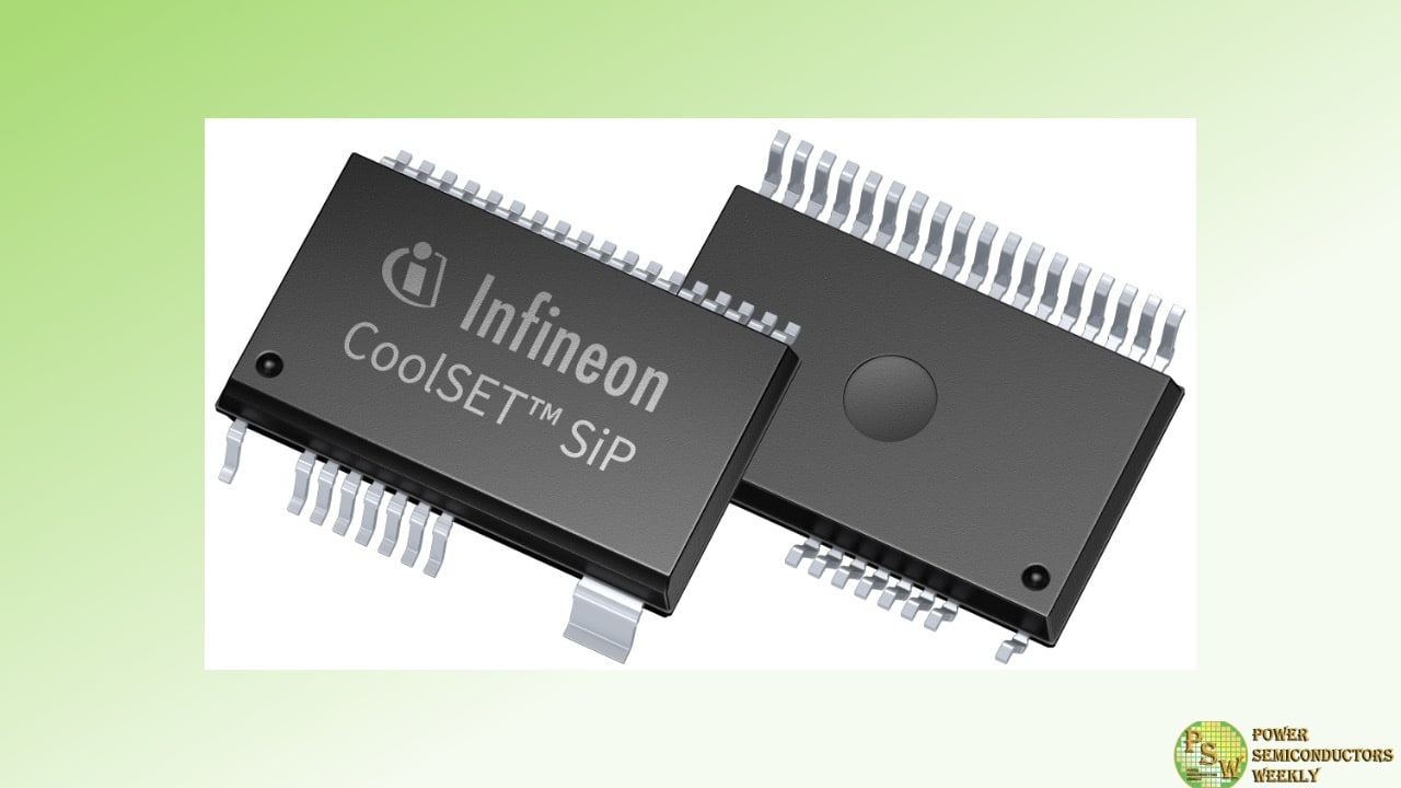
Infineon Technologies AG is launching its new CoolSET™ System in Package (SiP), a compact, fully integrated system power controller for highly efficient power delivery of up to 60 W at universal input voltage range of 85 – 305 V AC. Housed in a small SMD package, the high-voltage MOSFET with low R DS(ON) eliminates the need for an external heat sink, reducing system size and complexity.
The CoolSET SiP supports zero-voltage switching (ZVS) flyback operation, which enables low switching losses and low EMI signature, while also enhancing system reliability and robustness. This makes it an ideal solution for applications such as major home appliances and AI servers. In addition, the controller makes it easier for developers to meet stringent energy standards, supporting future-proof power solutions for modern designs.
The CoolSET SiP integrates a 950 V startup-cell, an 800 V avalanche rugged CoolMOS™ P7 SJ MOSFET, a ZVS primary flyback controller, a secondary-side synchronous rectification (SR) controller, and reinforced isolated communication enabled by Infineon’s proprietary CT Link technology. This high level of integration supports the development of more sophisticated end products by significantly reducing the number of discrete components, lowering the bill of materials, and minimizing PCB space requirements. A comprehensive set of advanced protection features simplifies system integration and allows designers more flexibility to optimize their solutions and enhance the overall user experience.
Infineon’s CoolSET System in Package (SiP) product samples are available to order. Infineon will show a demo version at PCIM Europe 2025. Further information is available at https://www.infineon.com/cms/en/product/promopages/coolset-sip/
Original – Infineon Technologies
-

Navitas Semiconductor announced a new family of GaNSense™ Motor Drive ICs targeting home appliances and industrial drives up to 600 W.
Specifically designed for motor drive applications, this fully integrated solution combines two GaN FETs in a half-bridge configuration with drive, control, sensing, and autonomous protection. Compared to legacy silicon IGBT solutions, this results in a 4% higher efficiency, 40% PCB footprint reduction, and 15% lower system cost.
Key features include bidirectional lossless current sensing, which measures both positive and negative currents. This is critical in motor drives, given recirculating currents in the reverse direction between switching coil phases. The lossless sensing eliminates the need for external shunt resistors, resulting in higher efficiency, improved reliability, and a more compact design.
Turn-on and turn-off slew rates are fully adjustable, allowing designers to optimize EMI, performance, and maximize efficiency. The autonomous freewheeling function switches on the GaN IC upon detection of reverse current to reduce conduction losses, maximize efficiency, and reduce the size and cost of heatsinks.
The GaNSense Motor Drive IC family also includes several safety features such as high-and-low-side short circuit protection, over-temperature protection (OTP), and 2kV ESD on all pins.
The 650V family starts with NV6257 (2 x 170 mΩ, PQFN 6×8), NV6287 (2 x 170 mΩ, PQFN 8×10), and NV6288 (2 x 120 mΩ, PQFN 8×10), supporting drives up to 600 W.
Target applications focus on motor drives up to 600W, including air conditioners, heat pumps, washing machines, dryers, dishwashers, refrigerators, and hair dryers. For low-power industrial drives, applications range from pumps to circulators and fans.
Original – Navitas Semiconductor
-

Alpha and Omega Semiconductor Limited (AOS) announced its AOTL66935 utilizes AOS’ 100V AlphaSGT™ proprietary MOSFET technology which combines the advantages of trench technology for low on-resistance with high safe operating area (SOA) capability that meets 48V hot swap requirements in AI server and telecom applications.
The AOTL66935 hot swap MOSFET prevents damage to the system by limiting the high inrush current with low power losses due to the very low on-resistance (RDS(ON)). These features help deliver increased performance and reliability in harsh application conditions required in latest AI server designs. The AOTL66935 is available in TO-Leadless (TOLL) package, which is 30% smaller footprint compared to TO-263 (D2PAK). AOTL66935 is manufactured in IATF 16949-certified facilities. TOLL package technology is compatible with automated optical inspection (AOI) manufacturing requirements.
“48V hot swap in AI servers requires a MOSFET that excels in high current capability while providing exceptional SOA robustness with high reliability. We designed the AOTL66935 to meet these demands, and the low on-resistance reduces the power losses and can enable less devices in parallel,” said Peter H. Wilson, Sr. Director of MOSFET product line at AOS.
Technical Highlights
Part Number Package VDS (V) VGS (±V) TJ (°C) Continuous Drain Current (A) Pulsed Drain Current (A) RDS(ON) Max (mOhms) @10V @25°C @100°C @25°C AOTL66935 TOLL 100 20 175 360 258 1440 1.95 Pricing and Availability
The AOTL66935 MOSFET is immediately available in production quantities with a lead time of 14-16 weeks. The unit price in 1,000-piece quantities is $4.2.
Original – Alpha and Omega Semiconductor
-

Alpha and Omega Semiconductor Limited (AOS) introduced the company’s next generation (Gen3) 1200V αSiC MOSFETs designed to maximize efficiency in a growing market of high power applications. These Gen3 MOSFETs provide up to 30 percent improved switching figure-of-merit (FOM) compared to AOS’ previous generation while maintaining low conduction losses at high load conditions. The performance improvements do not compromise ruggedness and reliability, as the Gen3 MOSFETs have full AEC-Q101 qualification, with extended lifetime and HV-H3TRB capabilities.
As power demands surge in electric vehicles (EVs), AI data centers, and renewable energy systems, inefficiencies in power conversion stages can significantly strain electrical supply and cooling systems. For EV designs, AOS’ Gen3 αSiC MOSFETs enable engineers to create higher power density systems with greater efficiency, reducing battery consumption and extending vehicle range. Future AI data centers adopting high-voltage DC (HVDC) architectures, such as 800V or ±400V, will benefit from reduced losses and increased power density to meet growing power requirements. To support these higher system voltages, AOS’ Gen3 1200V devices will be critical for enabling new topologies with the necessary efficiency.
The new AOS Gen3 1200V MOSFETs are available with an on-resistance (Rds(on)) range from 15mOhm (AOM015V120X3Q) to 40mOhm (AOM040V120X3Q) in a TO27-4L package. AOS plans to roll out its Gen3 MOSFETs in additional surface mount and topside cooled packages as well as in case modules. AOS has also qualified a larger Gen3 1200V/11mOhm MOSFET die designed for high-power EV traction inverter modules and is available for wafer sales.
“Electric vehicles and AI are transforming industries, but they require advanced power systems that can maintain efficiency even as energy demands increase,” said David Sheridan, Vice President of Wide Bandgap products at AOS. “We’re excited that this next generation of AOS αSiC MOSFETs can deliver the performance our customers require while making a positive environmental impact.”
Technical Highlights
- Automotive AEC-Q101 Qualified
- Wide compatibility of gate drive voltages (+15V to +18V)
- Up to 30% improved switching FOM
- Extended HV-H3TRB compliant
- Improved UIS and Short Circuit Capability
Original – Alpha and Omega Semiconductor
-

Infineon Technologies AG provides its 600 V CoolMOS™ 8 high-voltage superjunction (SJ) MOSFET product family to LITEON, a leader in power management solutions, for superior efficiency and reliability in server applications. The 600 V CoolMOS 8 offers an all-in-one solution that improves LITEON’s new generation technology for existing and upcoming server application designs.
Infineon’s newest CoolMOS 8 at 600 V is leading the way in high-voltage superjunction MOSFET technology, setting the standard for both technology and price performance on a global scale. The technology increases the overall performance of systems, while also playing a crucial role in reducing carbon emissions in various applications, including chargers and adapters, solar and energy storage systems, EV charging infrastructure, and uninterruptible power supplies (UPS) for example.
The 600 V CoolMOS 8 SJ is designed to provide high efficiency and reliability, which aligns perfectly with LITEON’s and Infineon’s commitment to advancing performance and total-cost-of-ownership for server applications. Additionally, the .XT interconnect technology being a key feature of CoolMOS 8 makes the new generation a perfect fit for conventional and AI servers. The advanced interconnect technology offers industry leading thermal dissipation capabilities and improves electrical performance by reducing parasitic inductance and resistance. The CoolMOS 8 SJ MOSFETs have an 18 percent lower gate charge compared to previous MOSFET models and the quickest turn-off time in the market. Their thermal performance has been improved by 14 to 42 percent.
“Our CoolMOS 8 SJ MOSFETs achieve first-class power density and efficiency, which is essential for high-performance server applications,” said Richard Kuncic, Head of Power Systems at Infineon. “The all-in-one solution provided by the CoolMOS 8 product family simplifies our portfolio, making the selection process easier whilst reducing design-in efforts.”
“LITEON is excited to leverage Infineon’s CoolMOS 8 family in our next-generation server designs,” said John Chang, General Manager, Cloud Infrastructure Platform & Solution SBG, LITEON. “The superior efficiency and reliability of the 600 V CoolMOS 8 SJ underscores our commitment to delivering cutting-edge technology and energy-efficient solutions to our customers.”
The 600 V CoolMOS 8 SJ MOSFETs series is an “all in MOSFET” technology addressing industrial and consumer applications. Thanks to its integrated fast body diode, it enables usage of one MOSFET family across all main topologies in the targeted markets. It enables cost attractive Si-based solutions enhancing Infineon’s high-voltage wide band gap (WBG) offerings. The MOSFETs are available in SMD-QDPAK, TOLL and ThinTOLL-8×8 packages.
Samples of the 600 V CoolMOS 8 SJ MOSFETs are now available. More information is available at www.infineon.com/coolmos8. Learn more about the benefits of Infineon’s 600 V CoolMOS 8 SJ MOSFETs in the whitepaper here.
Original – Infineon Technologies
-

Infineon Technologies AG launched its new CoolSiC™ MOSFET 750 V G2 technology, designed to deliver improved system efficiency and increased power density in automotive and industrial power conversion applications. The CoolSiC MOSFETs 750 V G2 technology offers a granular portfolio with typical R DS(on) values up to 60 mΩ at 25°C, making it suitable for a wide range of applications, including on-board chargers (OBCs), DC-DC converters, auxiliaries for electric vehicles (xEVs) as well as industrial applications in EV charging, solar inverter, energy storage systems, telecom and SMPS.
The ultra-low R DS(on) values 4 and 7 mΩ enable outstanding performance in static-switching applications, making the MOSFETs a perfect choice for applications such as eFuse, high-voltage battery disconnect switches, solid-state circuit breakers, and solid-state relays. The best-in-class lowest R DS(on) 4 mΩ is featured in Infineon’s innovative top-side cooled Q-DPAK package, which is designed to provide optimal thermal performance and reliability.
The technology also exhibits excellent R DS(on) x Q OSS and best-in-class R DS(on) x Q fr, contributing to reduced switching loss in both hard-switching and soft-switching topologies with superior efficiency in hard-switching user cases. With reduced gate charge, the technology allows for faster switching and reduces gate drive losses, making them more efficient in high-frequency applications.
Additionally, the CoolSiC MOSFETs 750 V G2 offer a combination of high threshold voltage V GS(th),typ of 4.5 V at 25°C and ultra-low Q GD/Q GS ratio, which reinforce robustness against parasitic turn-on (PTO). Furthermore, the technology allows for extended gate driving capabilities, supporting static gate voltages of up to -7 V and transient gate voltages of up to -11 V. This enhanced voltage tolerance provides engineers with greater design margins and best compatibility with other devices in the market.
The CoolSiC 750 V G2 delivers unparalleled switching performance, great ease-of-use and superior reliability with firm adherence to AEC Q101 standards for automotive-grade parts and JEDEC standard for industrial-grade parts. It enables a more efficient, compact and cost-effective designs to fulfill the ever‑growing market needs and underscores its commitment to reliability and longevity in safety-critical automotive applications.
Infineon’s CoolSiC MOSFET 750 V G2 Q-DPAK 4/7/16/25/60 mΩ samples are available to order. More information is available at www.infineon.com/coolsic-750v
Original – Infineon Technologies
