-

Soitec announced its revenue for the fourth quarter of fiscal year 2025 and its full-year results of fiscal year 2025 (ended on March 31st, 2025). The financial statements were approved by the Board of Directors during its meeting.
Pierre Barnabé, Soitec’s CEO, commented: “On the back of strong sales in the fourth quarter, we closed fiscal year 2025 in line with our revised guidance, with a high-single digit decline in full-year revenue. In this context, strict cost management enabled us to deliver a robust EBITDA margin, generate positive free cash flow, and continue investing both in innovation and in our industrial capacity – all while maintaining a very healthy balance sheet.
In a volatile and uncertain economic environment, we are focusing on parameters within our control to strengthen our fundamentals and accelerate our diversification beyond RF-SOI and beyond Mobile Communications. With the growing adoption of our new products by industry leaders – POI becoming an industry standard for innovative smartphones and Photonics-SOI gaining traction among industry leaders to equip the next generation of AI Datacenters – we have been able to partially offset the ongoing RF-SOI inventory correction and mitigate the impact of the weakness in the automotive industry. While RF-SOI remains by far the first contributor to our revenue, three other products – FD-SOI, Power-SOI and POI – are now each generating around or above 100 million US dollars in revenue.
This environment however provides limited visibility. We have therefore decided to suspend all previously issued guidance and to only provide revenue guidance on a quarterly basis. We expect Q1’26 to reflect the impact of the Imager-SOI phase out, which we had already anticipated and prepared for. Q1’26 revenue is hence expected to be down around 20% year on year, Imager-SOI contributing 25 million dollars in Q1’25.
We remain confident in our solid fundamentals and in our ability to accelerate growth as soon as our end markets begin to recover. Our strong technology megatrends – 5G, Energy Efficiency and Artificial Intelligence – and our unique expertise in engineered substrates continue to support the expansion of our Addressable Market from around 5 million wafers (200-mm equivalent) in 2024 to around 12 million in 2030”, added Pierre Barnabé.
Original – Soitec
-

Texas Instruments (TI) announced it is working with NVIDIA in the development of power management and sensing technologies for 800V high-voltage direct current (HVDC) power distribution systems for data center servers. The new power architecture paves the way for more scalable and reliable next-generation AI data centers.
With the growth of AI, the power required per data center rack is predicted to increase from 100kW today to more than 1MW in the near future. To power a 1MW rack, today’s 48V distribution system would require almost 450lbs of copper, making it physically impossible for a 48V system to scale power delivery to support computing needs in the long term.
The new 800V high-voltage DC power-distribution architecture will provide the power density and conversion efficiency that future AI processors require, while minimizing the growth of the power supply’s size, weight and complexity. This 800V architecture will enable engineers to scale power-efficient racks as data-center demand evolves.
“A paradigm shift is happening right in front of our eyes,” said Jeffrey Morroni, director of power management research and development at Kilby Labs and a TI Fellow. “AI data centers are pushing the limits of power to previously unimaginable levels. A few years ago, we faced 48V infrastructures as the next big challenge. Today, TI’s expertise in power conversion combined with NVIDIA’s AI expertise is enabling 800V high-voltage DC architectures to support the unprecedented demand for AI computing.”
“Semiconductor power systems are an important factor in enabling high-performance AI infrastructure,” said Gabriele Gorla, VP of System Engineering of NVIDIA. “NVIDIA is teaming with suppliers to develop an 800V high-voltage DC architecture that will efficiently support the next generation of powerful, large-scale AI data centers.”
Original – Texas Instruments
-

Wolfspeed, Inc. announced that David Emerson, Ph.D. has been appointed Executive Vice President and Chief Operating Officer, a newly created role responsible for overseeing operational excellence across the Company’s 200-millimeter facility footprint, reducing customer lead times, and manufacturing leading silicon carbide solutions for Wolfspeed’s customers. Dr. Emerson will be responsible for Wolfspeed’s Operations, Supply Chain, and Quality divisions.
As the former Executive Vice President of our LED Products division, Dr. Emerson brings a proven track record of transforming complex, global operations into scaled and high-performing businesses that are positioned to win in emerging technologies. Notably, during his time at Wolfspeed (then operating as Cree, Inc.), Dr. Emerson gained an in-depth understanding of both the devices and materials businesses and helped guide the company through a period of heightened U.S. government scrutiny on global trade practices and fair competition.
Wolfspeed Chief Executive Officer, Robert Feurle, commented, “We are excited to welcome Dave back to Wolfspeed as our new Chief Operating Officer. Having previously led our LED business through market disruption and global expansion, Dave brings a wealth of industry expertise and strategic insight which positions him well to drive operational excellence at Wolfspeed. His ability to directly confront complex challenges aligns with our ambitions at this critical stage in Wolfspeed’s lifecycle. I look forward to collaborating with him as we work to reaccelerate revenue growth, work to achieve profitability, complete our 200-millimeter transition, and ultimately advance Wolfspeed’s global leadership in silicon carbide technology.”
“After spending a sizable portion of my career at Cree overseeing the development of silicon carbide-powered LED solutions, I am eager to contribute to Wolfspeed’s forward momentum as its new Chief Operating Officer. I am impressed by the Company’s sustained leadership in silicon carbide and its vertically integrated, greenfield 200-millimeter facility footprint,” said Dr. Emerson. “Under Robert’s leadership, Wolfspeed is increasingly focused on serving the fastest-growing areas of the silicon carbide market, and these strategic verticals necessitate high-performance, high-quality solutions. My experience driving operational excellence has equipped me with the skills to help develop best-in-class solutions for our blue-chip customers, all while working to accelerate the Company’s path to profitability. I’m excited for the opportunity to help shape the Company’s continued growth and success.”
The addition of the Chief Operating Officer role to the executive leadership team underscores Wolfspeed’s unwavering commitment to operational excellence as it scales its industry-leading 200 mm silicon carbide manufacturing platform. The Chief Operating Officer will play a critical role in driving manufacturing quality and efficiency. In this role, Dr. Emerson will also be responsible for accelerating time-to-market and ensuring consistent delivery of innovative, high-performance silicon carbide solutions to customers worldwide. As Wolfspeed continues to expand capacity to serve the expected growth in demand across automotive, industrial, and energy markets, this role is central to enhancing operational agility and achieving growth.
Original – Wolfspeed
-

Navitas Semiconductor announced a collaboration with NVIDIA on their next-generation 800 V HVDC architecture to support ‘Kyber’ rack-scale systems powering their GPUs, such as Rubin Ultra, enabled by GaNFast™ and GeneSiC™ power technologies.
NVIDIA’s next generation of 800V DC architecture aims to establish high-efficiency, scalable power delivery for next-generation AI workloads, to ensure greater reliability, efficiency, and reduced infrastructure complexity.
Today’s existing data center architecture uses traditional 54 V in-rack power distribution and is limited to a few hundred kilowatts (kW). Bulky copper busbars are required to transfer this low-voltage electricity from the rack-mounted power shelves to the compute trays. As power increases above 200 kW, this architecture runs into physical limits due to power density, copper requirements, and reduced system efficiency.
Modern AI data centers require gigawatts (GW) of power for the increasing demand for AI computation. Nvidia’s approach is to directly convert the 13.8 kV AC grid power to 800 V HVDC at the data center perimeter using solid state transformers (SST) and industrial-grade rectifiers, eliminating several AC/DC and DC/DC conversion steps, maximizing efficiency and reliability.
Due to the higher voltage level of 800 V HVDC, the thickness of copper wires can be reduced by up to 45%, due to I2R losses, where the same amount of power can be delivered with increased voltage and lower current. Using a traditional 54V DC system, over 200 kg of copper would be needed to power a 1MW rack, which is not sustainable for next-generation AI data centers with GW power demand.
The 800V HVDC directly powers the IT racks (eliminating the need for additional AC-DC converters) and is converted by DC-DC converters to lower voltages, which will drive GPUs, such as the Rubin Ultra.
Navitas is an established leader in AI data center solutions enabled by GaN and SiC technology. The high-power GaNSafe™ power ICs integrate control, drive, sensing, and critical protection features, enabling unprecedented reliability and robustness. GaNSafe is the world’s safest GaN with short-circuit protection (350ns max latency), 2kV ESD protection on all pins, elimination of negative gate drive, and programmable slew rate control. All these features are controlled with 4-pins, allowing the package to be treated like a discrete GaN FET, requiring no VCC pin.
Additionally, Navitas offers a family of medium voltage (80-120V) GaN devices, which have been optimized for secondary side DC-DC conversion, delivering high-speed, high efficiency, and small footprint, for AI data centers PSUs with outputs of 48V-54V.
Enabled by 20 years of SiC innovation leadership, GeneSiC proprietary ‘trench-assisted planar’ technology provides world-leading performance over temperature, delivering high-speed, cool-running operation for high-power, high-reliability applications. G3F SiC MOSFETs deliver high-efficiency with high-speed performance, enabling up to 25°C lower case temperature, and up to 3x longer life than SiC products from other vendors.
Offering the industry’s broadest voltage range – stretching from 650 V to ultra-high voltages of 2.3 kV to 6.5 kV, the SiC technology has been implemented in multiple projects for MW energy storage and grid-tied inverters with the Department of Energy (DoE).
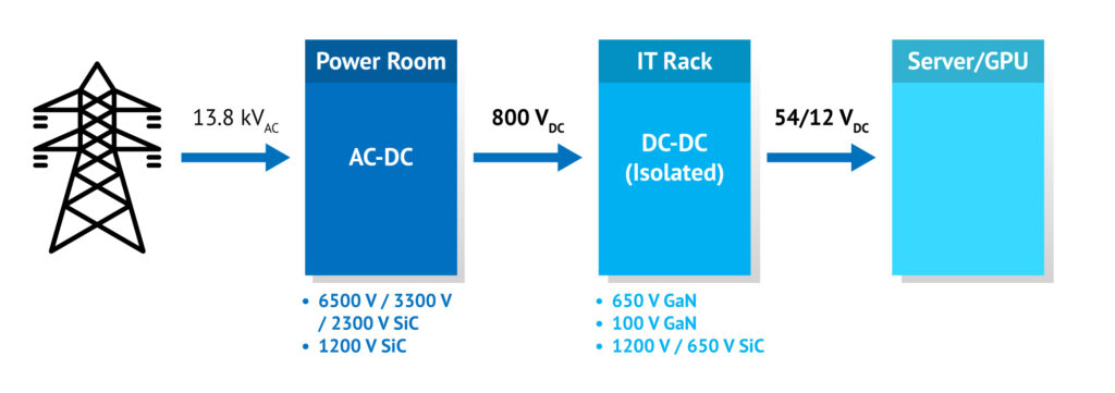
Fig. 1. Navitas GaN and SiC technologies cover the complete power delivery from grid to the GPU.
In August 2023, Navitas introduced a high-speed, high-efficiency 3.2 kW CRPS, achieving a 40% smaller size than best-in-class, legacy silicon solutions for power-hungry AI and Edge computing. This was followed by the world’s highest power density 4.5 kW CRPS, achieving a ground-breaking 137 W/in3, and an efficiency of over 97%. In November 2024, Navitas released the world’s first 8.5 kW AI data center power supply, powered by GaN and SiC that could meet 98% efficiency, complying with the Open Compute Project (OCP) and Open Rack v3 (ORv3) specifications. Additionally, Navitas created IntelliWeave, an innovative patented new digital control technique, that when combined with high-power GaNSafe and Gen 3-Fast SiC MOSFETs, enables PFC peak efficiencies to 99.3% and reduces power losses by 30% compared to existing solutions. Alongside the Computex exhibition in Taiwan, the latest release of their 12 kW PSU was presented at the Navitas ‘AI Tech Night’ on 21st May.
“We are proud to be selected by NVIDIA to collaborate on their 800 HVDC architecture initiative. Our latest innovations in high-power GaN and SiC technologies have seen world firsts and have created new inflections into markets such as AI datacenters and electric vehicles”, said Gene Sheridan, CEO and co-founder of Navitas. “With our wide portfolio range, we can support NVIDIA’s 800V HVDC infrastructure, from grid to the GPU. We appreciate that NVIDIA recognizes our technology and commitment to driving the next generation of data center power delivery.”
NVIDIA’s 800V HVDC architecture will improve end-to-end power efficiency up to 5%, reduce maintenance costs by 70% (due to fewer PSU failures), and lower cooling costs by directly connecting HVDC to the IT and compute racks.
Original – Navitas Semiconductor
-

Analog Devices, Inc. announced financial results for its fiscal second quarter 2025, which ended May 3, 2025.
- Revenue of $2.64 billion, with double-digit year-over-year growth across all end markets
- Operating cash flow of $3.9 billion and free cash flow of $3.3 billion on a trailing twelve-month basis or 39% and 34% of revenue, respectively
- Returned $0.7 billion to shareholders via dividends and repurchases during the second quarter
“ADI delivered second quarter revenue and earnings per share above the high end of guidance,” said Vincent Roche, CEO and Chair. “Against a backdrop of global trade volatility, our performance reflects the ongoing cyclical recovery, and the strength and resiliency of our business model. Our unwavering commitment to innovation and customer success, enables ADI to continue extending our leadership at the increasingly AI-driven Intelligent Edge, delivering exceptional value for shareholders over both the near- and long-terms.”
CFO Richard Puccio added, “Second quarter bookings accelerated across all end markets and all regions, resulting in continued sequential backlog growth. The improving demand signals we saw throughout our fiscal Q2, support our outlook for continued growth in Q3, and reinforce our view that we are in a cyclical upturn.”
Performance for the Second Quarter of Fiscal 2025 (PDF)
Outlook for the Third Quarter of Fiscal Year 2025
For the third quarter of fiscal 2025, we are forecasting revenue of $2.75 billion, +/- $100 million. At the midpoint of this revenue outlook, we expect reported operating margin of approximately 27.2%, +/-150 bps, and adjusted operating margin of approximately 41.5%, +/-100 bps. We are planning for reported EPS to be $1.23, +/-$0.10, and adjusted EPS to be $1.92, +/-$0.10.
Our third quarter fiscal 2025 outlook is based on current expectations and actual results may differ materially as a result of, among other things, the important factors discussed at the end of this release. The statements about our third quarter fiscal 2025 outlook supersede all prior statements regarding our business outlook set forth in prior ADI news releases, and ADI disclaims any obligation to update these forward-looking statements.
The adjusted results and adjusted anticipated results above are financial measures presented on a non-GAAP basis. Reconciliations of these non-GAAP financial measures to their most directly comparable GAAP financial measures are provided in the financial tables included in this release. See also the “Non-GAAP Financial Information” section for additional information.
Original – Analog Devices
-

Navitas Semiconductor has announced their latest 12 kW power supply unit (PSU) ‘designed for production’ reference design for hyperscale AI data centers with high-power rack densities of 120 kW.
The 12 kW PSU complies with Open Rack v3 (ORv3) specifications and Open Compute Project (OCP) guidelines. It utilizes Gen-3 Fast SiC MOSFETs, a novel ‘IntelliWeave™’ digital platform, and high-power GaNSafe ICs configured in 3-phase interleaved TP-PFC and FB-LLC topologies to ensure the highest efficiency and performance, with the lowest component count.
The 3-Phase interleaved totem-pole power factor correction (TP-PFC) is powered by Gen-3 Fast SiC MOSFETs with ‘trench-assisted planar’ technology, which has been enabled by over 20 years of SiC innovation leadership and offers world-leading performance over temperature, delivering cool-running, fast-switching, and superior robustness to support faster charging EVs and up to 3x more powerful AI data centers.
IntelliWeave digital control provides a hybrid control strategy of both Critical Conduction Mode (CrCM) and Continuous Conduction Mode (CCM), for light-load to full-load conditions, ensuring maximum efficiency while maintaining a simplistic design with low component count. This results in a 30% reduction in power losses compared to existing Continuous Conduction Mode (CCM) solutions.
The 3-phase interleaved full-bridge (FB) LLC topology is enabled by 4th generation high-power GaNSafe ICs, integrating control, drive, sensing, and critical protection features that allow unprecedented reliability and robustness. GaNSafe is the world’s safest GaN with short-circuit protection (350ns max latency), 2kV ESD protection on all pins, elimination of negative gate drive, and programmable slew rate control. All these features are controlled with four pins, allowing the package to be treated like a discrete GaN FET, requiring no VCC pin. Suitable for applications from 1 kW to 22 kW, 650 V GaNSafe in TOLL and TOLT packages are available with a range of RDS(ON)typ. from 18 to 70 mΩ.
The PSU is 790 x 73.5 x 40 mm and has an input voltage range of 180 – 305 VAC, outputting up to 50 VDC and delivering 12 kW when using input voltages above 207 VAC and 10 kW below this. Additionally, it implements active current sharing and over-current, over-voltage, under-voltage, and over-temperature protections. It has an operating temperature range of -5 to 45oC, a hold-up time of ³20 ms at 12 kW, and an inrush current of £3 times the steady-state current below 20 ms. Cooling is via the PSU’s internal fan.
“The continuation and leadership of Navitas’ AI power roadmap has seen a quadrupling in output power – from 2.7 to 12 kW – in just over 24 months,” said Gene Sheridan, CEO and co-founder of Navitas. “This increase in power delivery is vital for the world’s data centers to support the exponential power demanded by the latest GPU architectures. The ‘designed for production’ PSU enables our customers to quickly implement a highly efficient, simple, and cost-effective solution to address the power delivery challenges for AI and hyperscale data centers.”
The 12 kW PSU was presented at Navitas’ ‘AI Tech Night’ on 21st May, alongside the Computex exhibition in Taiwan.
Original – Navitas Semiconductor
-

Infineon Technologies AG is revolutionizing the power delivery architecture required for future AI data centers. In collaboration with NVIDIA, Infineon is developing the next generation of power systems based on a new architecture with central power generation of 800 V high-voltage direct current (HVDC).
The new system architecture significantly increases energy-efficient power distribution across the data center and allows power conversion directly at the AI chip (Graphic Processing Unit, GPU) within the server board. Infineon’s expertise in power conversion solutions from grid to core based on all relevant semiconductor materials silicon (Si), silicon carbide (SiC) and gallium nitride (GaN) is accelerating the roadmap to a full scale HVDC architecture.
This revolutionary step paves the way for the implementation of advanced power delivery architectures in accelerated computing data centers and will further enhance reliability and efficiency. As AI data centers already are going beyond 100,000 individual GPUs, the need for more efficient power delivery is becoming increasingly important. AI data centers will require power outputs of one megawatt (MW) and more per IT rack before the end of the decade. Therefore, the HVDC architecture coupled with high-density multiphase solutions will set a new standard for the industry, driving the development of high-quality components and power distribution systems.
“Infineon is driving innovation in artificial intelligence,” said Adam White, Division President Power & Sensor Systems at Infineon. “The combination of Infineon’s application and system know-how in powering AI from grid to core, combined with NVIDIA’s world-leading expertise in accelerated computing, paves the way for a new standard for power architecture in AI data centers to enable faster, more efficient and scalable AI infrastructure.”
“The new 800V HVDC system architecture delivers high reliability, energy-efficient power distribution across the data center,” said Gabriele Gorla, vice president of system engineering at NVIDIA. “Through this innovative approach, NVIDIA is able to optimize the energy consumption of our advanced AI infrastructure, which supports our commitment to sustainability while also delivering the performance and scalability required for the next generation of AI workloads.”
At present, the power supply in AI data centers is decentralized. This means that the AI chips are supplied with power by a large number of power supply units (PSU). The future system architecture will be centralized, making the best possible use of the constraint space in a server rack. This will increase the importance of leading-edge power semiconductor solutions using fewest power conversion stages and allowing upgrades to even higher distribution voltages.
Infineon is a leader in power semiconductor solutions and systems integration. The company expects the proportion of power semiconductors in a centralized HVDC architecture to be similar or higher than in today’s AC distribution architecture. Additionally, to the scaling of the HVDC power architecture, Infineon continues to support state of the art DCDC multiphase solutions and intermediate architectures for hyperscalers and AI data center operators with a broad product portfolio based on all relevant semiconductor materials along the entire power flow.
Learn more about Infineon’s AI power and data center solutions here.
Original – Infineon Technologies
-

Toshiba Electronic Devices & Storage Corporation (“Toshiba”) has launched four 650V silicon carbide (SiC) MOSFETs, equipped with its latest 3rd generation SiC MOSFET chips and housed in a compact DFN8×8 package, suitable for industrial equipment, such as switched-mode power supplies and power conditioners for photovoltaic generators. Volume shipments of the four devices, “TW031V65C,” “TW054V65C,” “TW092V65C,” and “TW123V65C,” start today.
The new products are the first 3rd generation SiC MOSFETs to use the small surface-mount DFN8×8 package, which reduces volume by more than 90% compared to lead-inserted packages, such as TO-247 and TO-247-4L(X) and improves equipment power density. Surface mounting also allows use of parasitic impedance components smaller than those of lead-inserted packages, reducing switching losses.
DFN8×8 is a 4-pin package, allowing use of a Kelvin connection of its signal source terminal for the gate drive. This reduces the influence of inductance in the source wire within the package, achieving high-speed switching performance; in the case of TW054V65C, it reduces turn-on loss by approximately 55% and turn-off loss by approximately 25% compared to current Toshiba products, helping to reduce power loss in equipment.
Toshiba will continue to expand its lineup to contribute to improved equipment efficiency and increased power capacity.
Applications
- Switched mode power supplies in servers, data centers, communications equipment, etc.
- EV charging stations
- Photovoltaic inverters
- Uninterruptible power supplies
Features
- DFN8×8 surface-mount package. Enables equipment miniaturization of and automated assembly. Low switching loss.
- Toshiba’s 3rd generation SiC MOSFETs
- Good temperature dependence of drain-source On-resistance by optimization of drift resistance and channel resistance ratio
- Low drain-source On-resistance×gate-drain charges
- Low diode forward voltage: VDSF=-1.35V(typ.) (VGS=-5V)
Original – Toshiba
-
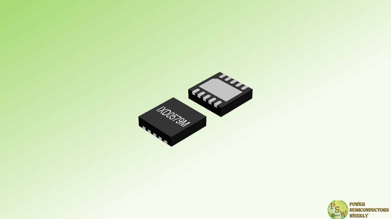
Littelfuse, Inc. announced the release of the IXD0579M high-speed gate driver IC. The IXD0579M simplifies board design, saves space, and offers a reliable, multiple-source alternative for driving N-channel MOSFETs or IGBTs in half-bridge configurations.
Designed to operate across a wide 6.5 V to 18 V supply range, the IXD0579M integrates a bootstrap diode and a series current limit resistor—components typically requiring discrete placement—into a single compact 3×3 mm² TDFN-10 package. This innovative integration reduces BOM count and cost while enabling easier PCB layout.
Key Product Features and Benefits
- High Drive Capability: 1.5 A source and 2.5 A sink output drive current
- Wide Supply Voltage Range: Operates from 6.5 V to 18 V with UVLO protection
- Integrated Bootstrap Circuitry: On-chip bootstrap diode and resistor simplify design
- Logic Level Compatibility: Interfaces directly with TTL and CMOS levels (down to 3.3 V)
- Cross-Conduction Protection: Prevents simultaneous high-side and low-side conduction
- Ultra-Low Standby Current: Less than 1 µA standby mode for energy efficiency
- Thermal Robustness: Operates from −40 °C to +125 °C
“With the IXD0579M, Littelfuse is offering a direct drop-in replacement for popular industry-standard gate driver ICs,” said June Zhang, Product Manager, Integrated Circuits Division at Littelfuse. “This gives customers greater flexibility to secure supply while simplifying their circuit design with an integrated solution.”
The IXD0579M is the first Littelfuse gate driver to feature both an integrated bootstrap diode and current limit resistor, expanding the company’s growing portfolio of power control solutions. As the eleventh high-side/low-side driver released by Littelfuse, it strengthens the company’s position in serving “multiple source” markets that demand performance and supply chain continuity.
Engineered for high-frequency switching, the IXD0579M is ideal for:
- Brushless DC (BLDC) motor drives
- Battery-powered hand tools
- DC-DC converters and power supplies
- General industrial and electrical equipment
It’s compact footprint and robust performance make it well-suited for space-constrained designs and high-efficiency power stages.
Original – Littelfuse
-
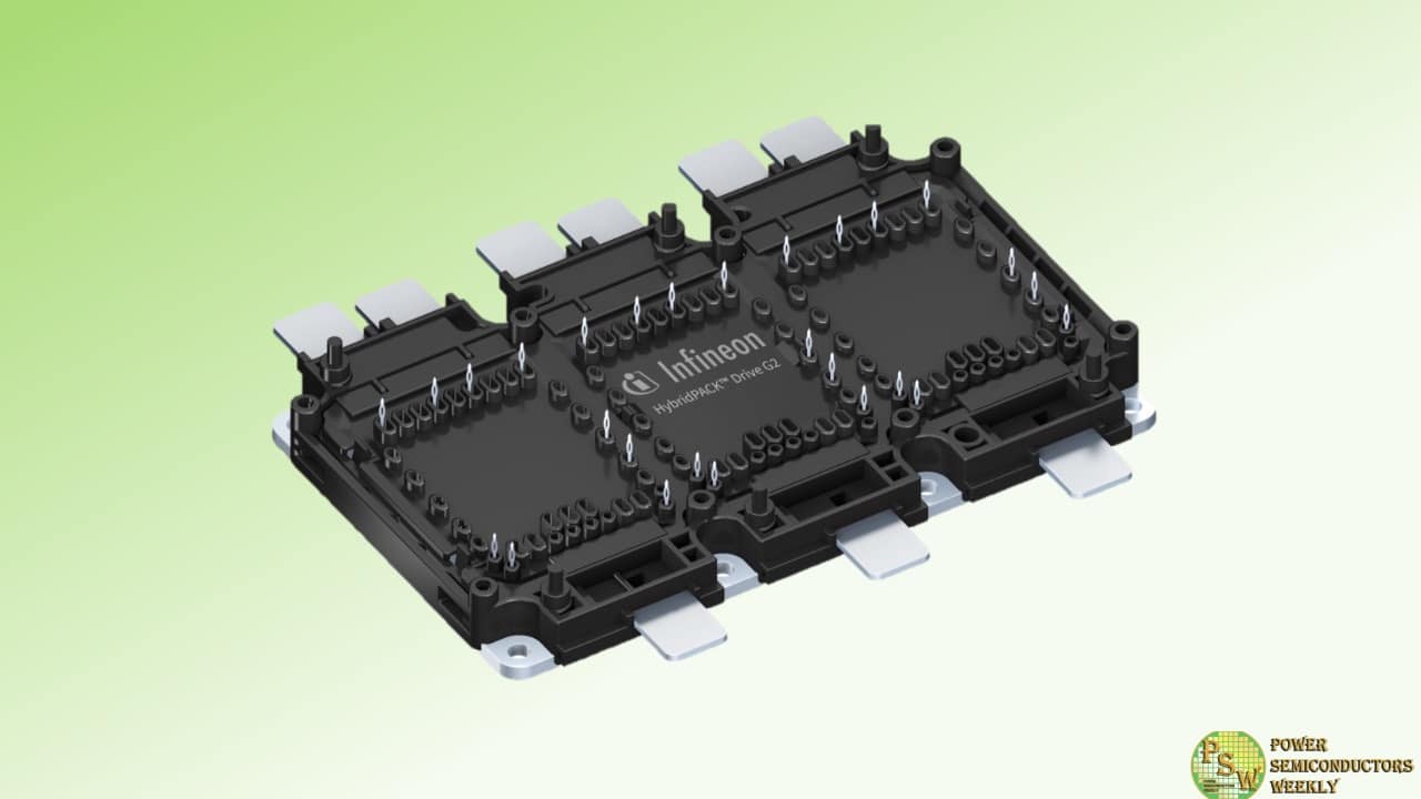
Infineon Technologies AG will supply Rivian’s R2 platform with power modules for traction inverters. The R2 platform will use silicon carbide (SiC) and silicon (Si) modules from Infineon’s HybridPACK™ Drive G2 family. Supply is expected to start in 2026. Additionally, Infineon will supply other products for the platform, including AURIX™ TC3x microcontrollers and power management ICs.
“We are committed to enhancing the performance and range of electric vehicles jointly with innovative automotive companies like Rivian,” said Stefan Obersriebnig, head of the product line for high voltage modules in Infineon’s Automotive Division. “Our dedication for innovation and zero-defect quality has made us the preferred partner of the automotive industry. With our broad product portfolio, system expertise and manufacturing capabilities, we are a key enabler of emission-free, sustainable mobility.”
HybridPACK Drive is Infineon’s market-leading power module family for electric vehicles. With more than 10.5 million units sold since 2017, it contributes significantly to the transition to electromobility. This transition will lead to strong market growth for power semiconductors, especially those based on wide bandgap materials like SiC.
With the expansion of its Kulim fab, Infineon is building the world’s most competitive 200-millimeter SiC power fab and further strengthens its market-leading role as a high-quality, high-volume supplier to the automotive industry. As “Infineon One Virtual Fab” for highly innovative wide bandgap (WBG) technologies, Infineon’s production sites in Kulim and Villach share technologies and processes. This allows for fast ramping and smooth and highly efficient operations in SiC and gallium nitride (GaN) manufacturing and reinforces Infineon’s technological leadership across the spectrum of all power semiconductor materials, in silicon as well as SiC and GaN.
Original – Infineon Technologies
