-

Navitas Semiconductor announced its partnership with BrightLoop supporting their latest series of hydrogen fuel-cell chargers with automotive qualified Gen 3 ‘Fast’ SiC (G3F) MOSFETs for heavy-duty agricultural transportation equipment.
BrightLoop offers leading-edge, top-performance solutions with power conversion efficiencies over 98% and extreme power densities up to 35 kW/kg and 60 kW/L. Their high-voltage, high-power multiverters paired to BrightLoop’s Power Flow Processor technology are designed to deliver exceptional performance in both AC and DC applications, such as energy management scenarios for fuel cells and heavy-duty applications, as well as HV network adaptation.
Navitas’ auto-qualified G3F SiC MOSFETs are incorporated into BrightLoop’s 250 kW HV-DC/DC converter, with an output of 950VDC at 480A, and can be paralleled to achieve megawatt power capability.
Enabled by 20 years of SiC innovation leadership, GeneSiC proprietary ‘trench-assisted planar’ technology provides world-leading performance over temperature, delivering high-speed, cool-running operation for high-power, high-reliability applications. G3F SiC MOSFETs deliver high-efficiency with high-speed performance, enabling up to 25°C lower case temperature, and up to 3x longer life than SiC products from other vendors.
Trench-assisted planar technology enables an extremely low RDS(ON) increase versus temperature, which results in the lowest power losses across the complete operating range and offers up to 20% lower RDS(ON) under real-life operation at high temperatures compared to competition. All GeneSiC MOSFETs have the highest-published 100%-tested avalanche capability, 30% longer short-circuit withstand time, and tight threshold voltage distributions for easy paralleling.
“We are proud to partner with BrightLoop, the established leaders in leading-edge high-power density and efficiency converters,” said Gene Sheridan, CEO and co-founder of Navitas. “Both companies provide the technology and system leadership to enable the roadmap for next generation, high-power density, high-reliability converter solutions”.
“Navitas offers leading-edge SiC technology where efficiency, ruggedness, and reliability are paramount. Our high power-density, smart, efficient, and scalable multiverters lead the industry by enhancing the quantity and quality of energy delivered to our customers”, said Florent Liffran, CEO and founder of BrightLoop.
Original – Navitas Semiconductor
-

Infineon Technologies AG announced the first of a new family of radiation hardened Gallium Nitride (GaN) transistors, fabricated at Infineon’s own foundry, based on its proven CoolGan™ technology. Designed to operate in harsh space environments, the company’s new product is the first in-house manufactured GaN transistor to earn the highest quality certification of reliability assigned by the United States Defense Logistics Agency (DLA) to the Joint Army Navy Space (JANS) Specification MIL-PRF-19500/794.
The new radiation hardened GaN High Electron Mobility Transistor (HEMT) devices are engineered for mission-critical applications required in on-orbit space vehicles, manned space exploration, and deep space probes. Combining the robust performance of GaN HEMTs with Infineon 50+ years of experience in high reliability applications, the new power transistors deliver best-in-class efficiency, thermal management and power density for smaller, lighter, and more reliable space designs. The devices complement Infineon’s proven legacy radiation hardened silicon MOSFET portfolio, providing customers with access to a full catalog of power solutions for space applications.
“The Infineon team continues to push the limits of power design with our new GaN transistor line,” said Chris Opoczynski, Senior Vice President and General Manager HiRel, at Infineon. “This milestone brings the next-generation of high reliability power solutions for mission-critical defense and space applications that utilize the superior material properties of wide bandgap semiconductors to customers serving the growing aerospace market.”
The first three product variations in the new radiation hardened GaN transistor line are 100 V, 52 A devices featuring an industry leading (R DS(on) (drain source on resistance) of 4 mΩ (typical) and total gate charge (Qg) of 8.8 nC (typical). Encased in robust hermetically sealed ceramic surface mount packages, the transistors are Single Event Effect (SEE) hardened up to LET (GaN) = 70 MeV.cm2/mg (Au ion). Two devices, which are not JANS certified, are screened to a Total Ionizing Dose (TID) of 100 krad and 500 krad. The third device, screened to 500 krad TID, is qualified to the rigorous JANS Specification MIL-PRF-19500/794.
Infineon is the first company in the industry to achieve the DLA JANS certification for fully internally manufactured GaN power devices. DLA JANS certification requires rigorous levels of screening and Quality of Service Class Identifiers to ensure the performance, quality, and reliability required for space flight applications – making Infineon a leader in GaN for high reliability applications. Infineon is also running multiple lots prior to full JANS production release to ensure long term manufacturing reliability.
Engineering samples and evaluation boards are available immediately with the final JANS device being released in the summer of 2025. Additional JANS parts are launching soon, expanding available voltages and currents to enable customers greater flexibility in creating efficient and reliable designs. For more information, visit www.infineon.com/radhardgan
Original – Infineon Technologies
-

Navitas Semiconductor has announced their latest 12 kW power supply unit (PSU) ‘designed for production’ reference design for hyperscale AI data centers with high-power rack densities of 120 kW.
The 12 kW PSU complies with Open Rack v3 (ORv3) specifications and Open Compute Project (OCP) guidelines. It utilizes Gen-3 Fast SiC MOSFETs, a novel ‘IntelliWeave™’ digital platform, and high-power GaNSafe ICs configured in 3-phase interleaved TP-PFC and FB-LLC topologies to ensure the highest efficiency and performance, with the lowest component count.
The 3-Phase interleaved totem-pole power factor correction (TP-PFC) is powered by Gen-3 Fast SiC MOSFETs with ‘trench-assisted planar’ technology, which has been enabled by over 20 years of SiC innovation leadership and offers world-leading performance over temperature, delivering cool-running, fast-switching, and superior robustness to support faster charging EVs and up to 3x more powerful AI data centers.
IntelliWeave digital control provides a hybrid control strategy of both Critical Conduction Mode (CrCM) and Continuous Conduction Mode (CCM), for light-load to full-load conditions, ensuring maximum efficiency while maintaining a simplistic design with low component count. This results in a 30% reduction in power losses compared to existing Continuous Conduction Mode (CCM) solutions.
The 3-phase interleaved full-bridge (FB) LLC topology is enabled by 4th generation high-power GaNSafe ICs, integrating control, drive, sensing, and critical protection features that allow unprecedented reliability and robustness. GaNSafe is the world’s safest GaN with short-circuit protection (350ns max latency), 2kV ESD protection on all pins, elimination of negative gate drive, and programmable slew rate control. All these features are controlled with four pins, allowing the package to be treated like a discrete GaN FET, requiring no VCC pin. Suitable for applications from 1 kW to 22 kW, 650 V GaNSafe in TOLL and TOLT packages are available with a range of RDS(ON)typ. from 18 to 70 mΩ.
The PSU is 790 x 73.5 x 40 mm and has an input voltage range of 180 – 305 VAC, outputting up to 50 VDC and delivering 12 kW when using input voltages above 207 VAC and 10 kW below this. Additionally, it implements active current sharing and over-current, over-voltage, under-voltage, and over-temperature protections. It has an operating temperature range of -5 to 45oC, a hold-up time of ³20 ms at 12 kW, and an inrush current of £3 times the steady-state current below 20 ms. Cooling is via the PSU’s internal fan.
“The continuation and leadership of Navitas’ AI power roadmap has seen a quadrupling in output power – from 2.7 to 12 kW – in just over 24 months,” said Gene Sheridan, CEO and co-founder of Navitas. “This increase in power delivery is vital for the world’s data centers to support the exponential power demanded by the latest GPU architectures. The ‘designed for production’ PSU enables our customers to quickly implement a highly efficient, simple, and cost-effective solution to address the power delivery challenges for AI and hyperscale data centers.”
The 12 kW PSU was presented at Navitas’ ‘AI Tech Night’ on 21st May, alongside the Computex exhibition in Taiwan.
Original – Navitas Semiconductor
-

Toshiba Electronic Devices & Storage Corporation (“Toshiba”) has launched four 650V silicon carbide (SiC) MOSFETs, equipped with its latest 3rd generation SiC MOSFET chips and housed in a compact DFN8×8 package, suitable for industrial equipment, such as switched-mode power supplies and power conditioners for photovoltaic generators. Volume shipments of the four devices, “TW031V65C,” “TW054V65C,” “TW092V65C,” and “TW123V65C,” start today.
The new products are the first 3rd generation SiC MOSFETs to use the small surface-mount DFN8×8 package, which reduces volume by more than 90% compared to lead-inserted packages, such as TO-247 and TO-247-4L(X) and improves equipment power density. Surface mounting also allows use of parasitic impedance components smaller than those of lead-inserted packages, reducing switching losses.
DFN8×8 is a 4-pin package, allowing use of a Kelvin connection of its signal source terminal for the gate drive. This reduces the influence of inductance in the source wire within the package, achieving high-speed switching performance; in the case of TW054V65C, it reduces turn-on loss by approximately 55% and turn-off loss by approximately 25% compared to current Toshiba products, helping to reduce power loss in equipment.
Toshiba will continue to expand its lineup to contribute to improved equipment efficiency and increased power capacity.
Applications
- Switched mode power supplies in servers, data centers, communications equipment, etc.
- EV charging stations
- Photovoltaic inverters
- Uninterruptible power supplies
Features
- DFN8×8 surface-mount package. Enables equipment miniaturization of and automated assembly. Low switching loss.
- Toshiba’s 3rd generation SiC MOSFETs
- Good temperature dependence of drain-source On-resistance by optimization of drift resistance and channel resistance ratio
- Low drain-source On-resistance×gate-drain charges
- Low diode forward voltage: VDSF=-1.35V(typ.) (VGS=-5V)
Original – Toshiba
-
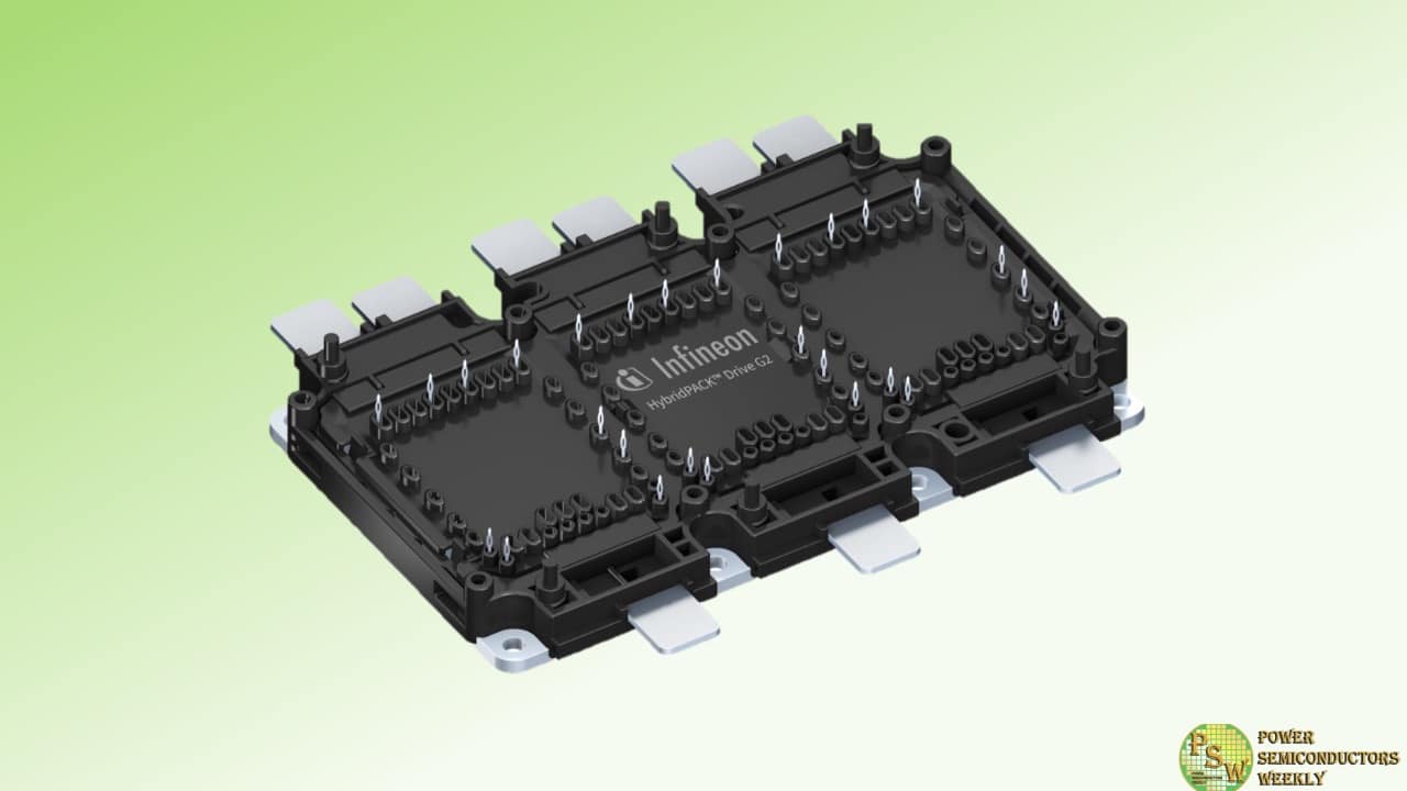
Infineon Technologies AG will supply Rivian’s R2 platform with power modules for traction inverters. The R2 platform will use silicon carbide (SiC) and silicon (Si) modules from Infineon’s HybridPACK™ Drive G2 family. Supply is expected to start in 2026. Additionally, Infineon will supply other products for the platform, including AURIX™ TC3x microcontrollers and power management ICs.
“We are committed to enhancing the performance and range of electric vehicles jointly with innovative automotive companies like Rivian,” said Stefan Obersriebnig, head of the product line for high voltage modules in Infineon’s Automotive Division. “Our dedication for innovation and zero-defect quality has made us the preferred partner of the automotive industry. With our broad product portfolio, system expertise and manufacturing capabilities, we are a key enabler of emission-free, sustainable mobility.”
HybridPACK Drive is Infineon’s market-leading power module family for electric vehicles. With more than 10.5 million units sold since 2017, it contributes significantly to the transition to electromobility. This transition will lead to strong market growth for power semiconductors, especially those based on wide bandgap materials like SiC.
With the expansion of its Kulim fab, Infineon is building the world’s most competitive 200-millimeter SiC power fab and further strengthens its market-leading role as a high-quality, high-volume supplier to the automotive industry. As “Infineon One Virtual Fab” for highly innovative wide bandgap (WBG) technologies, Infineon’s production sites in Kulim and Villach share technologies and processes. This allows for fast ramping and smooth and highly efficient operations in SiC and gallium nitride (GaN) manufacturing and reinforces Infineon’s technological leadership across the spectrum of all power semiconductor materials, in silicon as well as SiC and GaN.
Original – Infineon Technologies
-

Navitas Semiconductor will host an “AI Tech Night” event in Taipei, Taiwan, bringing together industry experts, supply chain partners, and technology developers for keynote speeches, demonstrations, and interactive discussions. The event will focus on how high-power GaNSafe™ and GeneSiC™ technologies are transforming AI data center infrastructure by overcoming efficiency and power density challenges to meet the growing power demands of AI and hyperscale data centers. Navitas will debut its next-generation OCP data center power supply unit (PSU) reference design, which has been ‘designed for production’ and achieves the world’s highest power density, performance, and efficiency.
With each GPU power exceeding 1,000W and AI cluster computing demand doubling every three months, traditional power supply technologies are struggling to keep pace with the evolving needs for energy efficiency and power density in AI infrastructure. Navitas’ GaN and SiC solutions will showcase the breakthrough of conventional architectural limitations and enable more efficient, high-density, and sustainable data center development.
Navitas ‘AI Power Roadmap’ was created in 2023, focusing on next-generation AI data center power delivery. The initial PSU was a high-speed, high-efficiency 2.7 kW CRPS (common redundant power supply), which offered 2x higher power density and a 30% reduction in energy loss. A 3.2kW CRPS followed, achieving a 40% smaller size than best-in-class, legacy silicon solutions for power-hungry AI and Edge computing. Next was the world’s highest-power-density 4.5kW CRPS, achieving 137W/in3 and an efficiency of over 97%. In November 2024, Navitas released the world’s first 8.5kW AI data-center power supply powered by GaN and SiC that could meet 98% efficiency, complying with the Open Compute Project (OCP) and Open Rack v3 (ORv3) specifications. Additionally, Navitas created IntelliWeave, a patented new digital control technique that, when combined with high-power GaNSafe and Gen 3-Fast SiC MOSFETs, enables PFC peak efficiencies of 99.3% and reduces power losses by 30% compared with existing solutions.
Navitas will also highlight the world’s first mass-produced 650V Bi-Directional GaNFast™ power ICs and IsoFast™ high-speed isolated gate drivers. These technologies drive a paradigm shift from traditional two-stage to single-stage power topologies, optimizing data center power supply design, reducing form factors, and increasing rack space utilization.
“The exponential growth of AI computing power poses stringent challenges for data center infrastructure. The debut of our latest AI data center PSU achieves dual breakthroughs in efficiency and power density, demonstrating Navitas’ continuous innovation in GaN and SiC technologies and deep understanding of the data center industry”, said Charles Zha, SVP and APAC GM of Navitas. “With years of focus on the Asia-Pacific market, we remain committed to aligning cutting-edge technologies with local needs and industry strengths. We look forward to collaborating with industry partners to explore how GaN and SiC innovation can drive efficiency and density upgrades in AI data centers, ensuring computing development progresses along with a sustainable future.”
The “AI Tech Night” will take place on May 21st, 2025, 6:30 pm-9:00 pm, at the Courtyard by Marriott Taipei. To participate in the ‘AI Tech Night’ event, please contact info@navitassemi.com.
Original – Navitas Semiconductor
-

Infineon Technologies AG has introduced the CoolGaN™ bidirectional switch (BDS) 650 V G5, a gallium nitride (GaN) switch capable of actively blocking voltage and current in both directions. Featuring a common-drain design and a double-gate structure, it leverages Infineon’s robust gate injection transistor (GIT) technology to deliver a monolithic bidirectional switch, enabled by Infineon’s CoolGaN technology. The device serves as a highly efficient replacement for traditional back-to-back configurations commonly used in converters.
The bidirectional CoolGaN switch offers several key advantages for power conversion systems. By integrating two switches in a single device, it simplifies the design of cycloconverter topologies, enabling single-stage power conversion, eliminating the need for multiple conversion stages. This leads to improved efficiency, increased reliability, and a more compact design. BDS-based microinverters also benefit from higher power density and reduced component count, which simplifies manufacturing and reduces costs. Additionally, the device supports advanced grid functions such as reactive power compensation and bidirectional operation.
As a result, this solution holds significant potential across a wide range of applications, including:
Microinverters: The CoolGaN bidirectional switch enables simpler and more efficient microinverter designs, reducing both size and cost. This makes microinverters more attractive for residential and commercial solar installations.
Energy Storage Systems (ESS): In ESS applications such as battery chargers and dischargers, the switch allows for more efficient and reliable energy storage and release.
Electric Vehicle (EV) Charging: In EV charging systems, the BDS switch supports faster, more efficient charging while also enabling vehicle-to-grid (V2G) functionality, where energy stored in the vehicle battery can be fed back into the grid.
Motor control: The CoolGaN BDS is ideal for use in Current Source Inverters (CSI) for industrial motor drives. Compared to traditional Voltage Source Inverters (VSI), CSIs offer benefits such as:
- Producing a sinusoidal output voltage, which supports longer cable runs, reduced losses, and improved fault tolerance.
- Replacing the DC-link capacitor with an inductor, improving high-temperature performance and short-circuit protection.
- Higher efficiency at partial loads, lower EMI, inherent buck-boost capability for voltage variation, and scalability for parallel operation.
These features make CSIs a more robust and efficient alternative for industrial motor applications.
AI data centers: In AI server power supplies, bidirectional switches like CoolGaN support higher switching frequencies and power density in architectures such as Vienna rectifiers and H4 PFCs. A single CoolGaN BDS can replace two conventional switches, reducing component count, cost, size, and overall power losses.
The CoolGaN bidirectional switch (BDS) 650 V G5 is available for ordering now as well as samples of the 110 mΩ product. More information is available here.
Original – Infineon Technologies
-

To enable the next generation of solid-state power distribution systems, Infineon Technologies AG is expanding its silicon carbide (SiC) portfolio with the new CoolSiC™ JFET product family. The new devices deliver minimized conduction losses, solid turn-off capability, and high robustness, making them ideal for advanced solid-state protection and distribution.
With robust short-circuit capability, thermal stability in linear mode, and precise overvoltage control, CoolSiC JFETs enable reliable and efficient system performance in a wide range of industrial and automotive applications, including solid-state circuit breakers (SSCBs), AI data center hot-swaps, eFuses, motor soft starters, industrial safety relays, and automotive battery disconnect switches.
“With CoolSiC JFET, we are addressing the growing demand for smarter, faster, and more robust power distribution systems,” says Dr. Peter Wawer, Division President Green Industrial Power at Infineon Technologies. “This application-driven power semiconductor technology is specifically designed to provide our customers with the tools they need to solve the complex challenges in this rapidly evolving space. We are proud to introduce devices that achieve best-in-class R DS(ON), setting a new standard for SiC performance and reaffirming Infineon’s leadership in the field of wide-bandgap technology.”
The first generation of CoolSiC JFETs features ultra-low R DS(ON) starting at 1.5 mΩ (750 V BDss) and 2.3 mΩ (1200 V BDss), significantly reducing conduction losses. The bulk-channel optimized SiC JFET offers high robustness under short-circuit and avalanche failure conditions. Housed in a Q-DPAK top-side cooled package, the devices support easy paralleling and scalable current handling, enabling compact, high-power systems with flexible layout and integration options. Their predictable switching behavior under thermal stress, overload and fault conditions provides maximum long-term reliability in continuous operation.
To meet the thermal and mechanical challenges of harsh application environments, CoolSiC JFETs leverage Infineon’s advanced .XT interconnection technology with diffusion soldering. This significantly improves transient thermal impedance and robustness under pulsed and cyclic loads typical of industrial power systems. Tested and qualified under real-world operating conditions of solid-state power switches and based on the industry-standard Q-DPAK package, the devices enable quick and seamless design integration in both industrial and automotive applications.
Engineering samples of the new CoolSiC JFET family will be available later in 2025, with volume production starting in 2026. The product portfolio will be further expanded with a variety of packages and modules. The product family has been successfully demonstrated at the Infineon booth at PCIM Europe 2025 in Nuremberg. More information is available at www.infineon.com/jfet.
Original – Infineon Technologies
-

Infineon Technologies AG and Visteon Corporation, a global leader in automotive cockpit electronics, announced the companies have signed a Memorandum of Understanding (MOU) to advance the development of next-generation electric vehicle powertrains.
In this joint effort, Infineon and Visteon will collaborate and integrate power conversion devices based on Infineon semiconductors, with particular emphasis on wideband gap device technologies, which provide significant advantages in power conversion applications compared to silicon-based semiconductors. These devices include greater power density, efficiency and thermal performance, which contribute to improved efficiency and reduced system costs for next-generation power conversion modules for the automotive sector.
Future Visteon EV powertrain applications incorporating Infineon CoolGaN™ (Gallium Nitride) and CoolSiC™ (Silicon Carbide) devices may include battery junction boxes, DC-DC converters and on-board chargers. The resulting powertrain systems will conform to the highest efficiency, robustness and reliability.
“Working with Infineon allows us to integrate cutting-edge semiconductor technologies that are essential in improving power conversion efficiency and overall system capability of next generation electric vehicles,” said Dr. Tao Wang, Head of the Electrification Product Line of Visteon Corporation. “This collaboration will advance technologies that accelerate the transition to a more sustainable and efficient mobility ecosystem.”
“Visteon is a recognized innovator and an early adopter of new technologies, making them an ideal partner for us,” said Peter Schaefer, Chief Sales Officer Automotive, Infineon Technologies AG. “Together, we will push the boundaries of electric vehicle technology and provide superior solutions to the global automotive industry.”
Original – Infineon Technologies
-

CISSOID and EDAG Group, a globally leading independent engineering services provider for the automotive industry, announced a strategic partnership aimed at accelerating the development of next-generation Silicon Carbide (SiC) traction inverters for electric mobility applications.
This collaboration brings together CISSOID’s cutting-edge expertise in SiC power semiconductor modules and control solutions with EDAG’s deep engineering know-how in the design, integration, and validation of electric powertrains. By combining their complementary strengths, the two companies aim to offer e-mobility OEMs and equipment suppliers unmatched technical support and complete solutions for the efficient, reliable, and functionally safe development of SiC-based traction inverters.
Key benefits of this partnership include:
- Joint development and integration of state-of-the-art SiC inverter platforms optimized for high-efficiency, high-power density, and extended operating life.
- Comprehensive engineering services covering inverter system design, thermal management, mechanical integration, functional safety and EMC compliance.
- Accelerated time-to-market through access to ready-to-implement, proven hardware and software solutions.
- End-to-end technical support, from concept design to prototyping and vehicle integration.
Pierre Delatte, CTO of CISSOID, stated: “This partnership with EDAG enables us to jointly address the growing demand for high-performance, SiC-based traction inverters. Together, we will help manufacturers harness the full potential of Silicon Carbide technology, making electric vehicles more efficient, compact, and reliable.”
Lennart Benthele, Head of Drivetrain & Thermal Development at EDAG, added: “At EDAG, we are committed to shaping the future of sustainable mobility. By partnering with CISSOID, we expand our capabilities in power electronics, offering our customers integrated solutions for the next generation of electric drivetrains.”
This collaboration marks a significant step forward in supporting the fast-evolving electric mobility market, where high-efficiency, compact, and robust inverter solutions are crucial to unlocking the full performance potential of modern EVs.
Original – CISSOID
