-

GlobalFoundries announced plans to invest $16 billion to expand its semiconductor manufacturing and advanced packaging capabilities across its facilities in New York and Vermont. GF’s investment is a strategic response to the explosive growth in artificial intelligence, which is accelerating demand for next-generation semiconductors designed for power efficiency and high-bandwidth performance across datacenters, communications infrastructure and AI-enabled devices.
GF is collaborating with major technology companies such as Apple, SpaceX, AMD, Qualcomm Technologies, Inc., NXP and GM, that are committed to reshoring semiconductor production to the U.S. and diversifying their global supply chains. These companies partner with GF to support their production of U.S.-made chips, underscoring GF’s role as a trusted supplier of essential semiconductors and a key enabler of supply chain security.
“At GlobalFoundries, we are proud to partner with pioneering technology leaders to manufacture their chips in the United States—advancing innovation while strengthening economic and supply chain resiliency,” said Tim Breen, CEO of GlobalFoundries. “The AI revolution is driving strong, durable demand for GF’s technologies that enable tomorrow’s datacenters – including GF’s leading silicon photonics, as well as GaN for power applications. Meanwhile at the edge, GF’s proprietary FDX technology is uniquely positioned to support AI functionality with low power consumption. With all these technologies and more manufactured right here in the U.S., GF is proud to play its part in accelerating America’s semiconductor leadership.”
“GlobalFoundries investment is a great example of the return of United States manufacturing for critical semiconductors,” said U.S. Secretary of Commerce, Howard Lutnick. “President Trump has made it a fundamental objective to bring semiconductor manufacturing home to America. Our partnership with GlobalFoundries will secure U.S. semiconductor foundry capacity and technology capabilities for future generations.”
The rapid rise of AI in both the cloud and at the edge is driving the adoption of new technology platforms and 3D heterogeneous integration technologies. These advanced solutions are essential to meet the exponentially growing requirements for power efficiency, bandwidth density and performance. GF is uniquely positioned to lead in this space, with its 22FDX® and silicon photonics capabilities in production in New York and advanced development of differentiated GaN-based power solutions in Vermont.
GF’s investment builds upon the company’s existing U.S. expansion plans, including more than $13 billion to expand and modernize its New York and Vermont facilities and funding for its recently launched New York Advanced Packaging and Photonics Center—the first U.S.-based facility of its kind dedicated to silicon photonics packaging. GF is committing an additional $3 billion, which includes advanced research and development initiatives focused on packaging innovation, silicon photonics and next-generation GaN technologies. In aggregate, these investments represent a $16 billion plan to strengthen U.S. semiconductor leadership and accelerate innovation in AI, aerospace, automotive and high-performance communications.
“Today’s announcement is a direct result of President Trump’s leadership and his vision to bring back high-paying manufacturing jobs and reestablish secure, domestic supply chains for critical technologies,” said Dr. Thomas Caulfield, Executive Chairman of GlobalFoundries. “We look forward to continuing to work with the U.S. government to help create the conditions for industry and government to work together and drive meaningful, long-term impact.”
“GlobalFoundries has supplied semiconductors for Apple products since 2010 and we’re excited to see them expand right here in the United States. These chips are an essential part of Apple products like iPhone, and they’re a powerful example of American manufacturing leadership.”
Tim Cook, Apple’s CEO
“Advanced semiconductors are critical to the advanced satellite capabilities which SpaceX has been pioneering for over two decades. We are excited by the expansion of GlobalFoundries’ manufacturing base right here in the U.S., which is core to Starlink’s growth and our commitment to manufacturing in the U.S., as well as our mission to deliver high-speed internet access to millions of people around the world.”
Gwynne Shotwell, president and COO at SpaceX
“As a valued technology partner, we’re pleased to see GlobalFoundries deepen its commitment to U.S. manufacturing. These efforts are critical to building a secure and resilient semiconductor supply chain in the U.S. to support the next wave of innovation in our industry.”
Dr. Lisa Su, AMD Chair and CEO
“As a strategic supplier of Qualcomm, GlobalFoundries shares our vision for strengthening U.S. chip production capacity. This commitment from GlobalFoundries will help secure a resilient semiconductor supply chain to support the next wave of U.S. technology innovation, especially in areas vital to enabling power efficient computing, connectivity, and edge intelligence.”
Cristiano Amon, president and CEO of Qualcomm Incorporated
“Deepening our partnership with GlobalFoundries aligns with NXP’s hybrid manufacturing strategy, where we work with leading foundry partners to better serve our customers’ strategic technology, capacity and resilience needs. This collaboration allows us to scale efficiently, expand production in the U.S. and continue delivering for our customers. It’s a strong step forward in building a resilient, high-performing semiconductor supply chain in the United States.”
Kurt Sievers, chief executive officer of NXP Semiconductors
“Semiconductors are critical to the future of vehicles, and their importance will only grow. GlobalFoundries’ investment supports our work to secure a reliable, U.S.-based chip supply—essential for delivering the safety, infotainment and features our customers expect.”
Mark Reuss, president of General Motors
Original – GlobalFoundries
-

On May 15, GlobalWafers Co., Ltd. hosted U.S. Investment Accelerator Executive Director Michael Grimes, Taiwan Minister of Economic Affairs Kuo Jyh-huei, AIT Director Raymond Greene, ROC Taiwan’s Representative to the United States Alexander Yui, Sherman Mayor Shawn Teamann, and hundreds of customers, suppliers, and partners in Sherman, Texas to celebrate the Grand Opening of GlobalWafers America (GWA), the company’s newest and most advanced 300mm silicon wafer manufacturing facility.
GlobalWafers made the decision to build its flagship facility in the United States in May 2022 and held the groundbreaking ceremony in Sherman on December 2, 2022. To date, the US$3.5 billion project has created 1200 construction and 180 permanent jobs in North Texas and will employ up to 650 engineering, technical and operational professionals by the end of 2028.
During the celebration Chairperson Doris Hsu unexpectedly announced the company’s plan to further grow its U.S. manufacturing base, stating: “On the three-year anniversary of our decision to build GWA, I am pleased to announce GlobalWafers’ intention to expand our current U.S. investment by another $4 billion to reach $7.5 billion!” In alignment with growth in market demand- combined with an advantageous tariff structure favoring cost effective U.S. expansion- GlobalWafers expects to add phases 3 and 4 to its existing commitment in Sherman. As the only advanced wafer supplier manufacturing in the United States, this additional investment, bolstered by ongoing support from the U.S. Government and the Trump Administration, is expected to fully secure the advanced wafer supply needed to power a broad range of next-generation technologies and innovation.
On this point, GWC President Mark England noted: “GWA will fill a key vulnerability in the U.S. supply chain and help build a more complete and self-sufficient local semiconductor ecosystem — one that is more resilient and future-ready.” In fact, GWA is the only fully integrated advanced silicon wafer manufacturing facility participating in the U.S. Government’s CHIPS for America Program and is the first production line of its kind built in the United States in over 20 years.
Under the CHIPS Program- now part of President Trump’s new U.S. Investment Accelerator- the U.S. Department of Commerce is investing US$406 million in GlobalWafers’ new U.S. operations in a strategy to rebuild a key node of the U.S. semiconductor supply chain. At the event, U.S. Investment Accelerator Executive Director Michael Grimes observed: “GlobalWafers investment is a great example of the return of United States manufacturing in a critical industry. President Trump and Secretary Lutnick have made it a fundamental objective to bring semiconductor manufacturing home to America. Through our work with GWA, we are ensuring that the essential starting material for advanced chips is manufactured right here in United States. GlobalWafers current investment, together with its new commitment announced today, will secure U.S. wafer supply for generations to come.”
The City of Sherman, Grayson County, and the State of Texas have also provided important incentives in the form of land, direct grants, tax incentives and excellent manufacturing infrastructure. Chairperson Doris Hsu noted, “There is simply not a more welcoming location in all the United States for doing business than Texas, Grayson County and Sherman. They have worked strategically to build the Silicon Prairie and GWA is thrilled to be part of it.” Governor Greg Abbott remarked, “We are proud that GlobalWafers America is now calling Texas home. GWA is rounding out the already well-established Texas semiconductor ecosystem, setting Texas apart as the only state in the country with advanced silicon wafers.”
From construction to production, GlobalWafers has partnered with hundreds of best-in-class suppliers who have also brought advanced engineering systems, technology and business processes to the project. “Without construction partners, toolmakers and materials suppliers also pushing the edge of their capabilities, GWA would not be able to deliver the quality wafers our customers have come to expect from GlobalWafers,” said GWA VP of Operations Wyatt Watson. “The GWA project has brought out the best of our entire supply chain.”
GlobalWafers is one of five global suppliers of advanced semiconductor wafers and the only one expanding in the United States during this new era of supply chain regionalization. Along these lines, Ashlie Wallace, GlobalFoundries’ SVP of Global Supply Chain, echoed the sentiment of many customers noting, “As a longstanding strategic partner, we are pleased to see GlobalWafers increasing domestic supply of silicon wafers critical to the essential semiconductors we manufacture.”
300mm silicon wafers are the essential input used by foundries and integrated device manufacturers to produce leading-edge, mature-node, and memory chips. Silicon from GWC’s semiconductor wafers is found in essentially every device that powers modern life– from home appliances, automobiles and physical infrastructure to cell phones, computers, and AI applications.
Further to the strategic phase 3 & 4 expansion announced today, GWA’s new 142-acre campus in Sherman— designed to accommodate up to six phases — has space to add two additional phases and significantly grow capacity in lockstep with chip producers who have collectively announced over US$500 billion in new U.S. investments over the next decade.
As part of our core ESG commitment, GlobalWafers companies worldwide practice green manufacturing. Once fully ramped, GWA will run on 100% renewable energy to produce the world’s most advanced silicon wafers. Across the GlobalWafers family, we remain deeply committed to minimizing our environmental impact while enabling the next generation of semiconductor innovation.
GlobalWafers Co., Ltd., the world’s third largest supplier of semiconductor wafers, maintains 18 manufacturing and operational sites spanning three continents and nine countries. The company is one of the global leaders in semiconductor technology, providing innovative and advanced technology solutions to leading chip manufacturers to transform lives around the world.
Original – GlobalWafers
-

Texas Instruments (TI) announced it is working with NVIDIA in the development of power management and sensing technologies for 800V high-voltage direct current (HVDC) power distribution systems for data center servers. The new power architecture paves the way for more scalable and reliable next-generation AI data centers.
With the growth of AI, the power required per data center rack is predicted to increase from 100kW today to more than 1MW in the near future. To power a 1MW rack, today’s 48V distribution system would require almost 450lbs of copper, making it physically impossible for a 48V system to scale power delivery to support computing needs in the long term.
The new 800V high-voltage DC power-distribution architecture will provide the power density and conversion efficiency that future AI processors require, while minimizing the growth of the power supply’s size, weight and complexity. This 800V architecture will enable engineers to scale power-efficient racks as data-center demand evolves.
“A paradigm shift is happening right in front of our eyes,” said Jeffrey Morroni, director of power management research and development at Kilby Labs and a TI Fellow. “AI data centers are pushing the limits of power to previously unimaginable levels. A few years ago, we faced 48V infrastructures as the next big challenge. Today, TI’s expertise in power conversion combined with NVIDIA’s AI expertise is enabling 800V high-voltage DC architectures to support the unprecedented demand for AI computing.”
“Semiconductor power systems are an important factor in enabling high-performance AI infrastructure,” said Gabriele Gorla, VP of System Engineering of NVIDIA. “NVIDIA is teaming with suppliers to develop an 800V high-voltage DC architecture that will efficiently support the next generation of powerful, large-scale AI data centers.”
Original – Texas Instruments
-

Navitas Semiconductor announced a collaboration with NVIDIA on their next-generation 800 V HVDC architecture to support ‘Kyber’ rack-scale systems powering their GPUs, such as Rubin Ultra, enabled by GaNFast™ and GeneSiC™ power technologies.
NVIDIA’s next generation of 800V DC architecture aims to establish high-efficiency, scalable power delivery for next-generation AI workloads, to ensure greater reliability, efficiency, and reduced infrastructure complexity.
Today’s existing data center architecture uses traditional 54 V in-rack power distribution and is limited to a few hundred kilowatts (kW). Bulky copper busbars are required to transfer this low-voltage electricity from the rack-mounted power shelves to the compute trays. As power increases above 200 kW, this architecture runs into physical limits due to power density, copper requirements, and reduced system efficiency.
Modern AI data centers require gigawatts (GW) of power for the increasing demand for AI computation. Nvidia’s approach is to directly convert the 13.8 kV AC grid power to 800 V HVDC at the data center perimeter using solid state transformers (SST) and industrial-grade rectifiers, eliminating several AC/DC and DC/DC conversion steps, maximizing efficiency and reliability.
Due to the higher voltage level of 800 V HVDC, the thickness of copper wires can be reduced by up to 45%, due to I2R losses, where the same amount of power can be delivered with increased voltage and lower current. Using a traditional 54V DC system, over 200 kg of copper would be needed to power a 1MW rack, which is not sustainable for next-generation AI data centers with GW power demand.
The 800V HVDC directly powers the IT racks (eliminating the need for additional AC-DC converters) and is converted by DC-DC converters to lower voltages, which will drive GPUs, such as the Rubin Ultra.
Navitas is an established leader in AI data center solutions enabled by GaN and SiC technology. The high-power GaNSafe™ power ICs integrate control, drive, sensing, and critical protection features, enabling unprecedented reliability and robustness. GaNSafe is the world’s safest GaN with short-circuit protection (350ns max latency), 2kV ESD protection on all pins, elimination of negative gate drive, and programmable slew rate control. All these features are controlled with 4-pins, allowing the package to be treated like a discrete GaN FET, requiring no VCC pin.
Additionally, Navitas offers a family of medium voltage (80-120V) GaN devices, which have been optimized for secondary side DC-DC conversion, delivering high-speed, high efficiency, and small footprint, for AI data centers PSUs with outputs of 48V-54V.
Enabled by 20 years of SiC innovation leadership, GeneSiC proprietary ‘trench-assisted planar’ technology provides world-leading performance over temperature, delivering high-speed, cool-running operation for high-power, high-reliability applications. G3F SiC MOSFETs deliver high-efficiency with high-speed performance, enabling up to 25°C lower case temperature, and up to 3x longer life than SiC products from other vendors.
Offering the industry’s broadest voltage range – stretching from 650 V to ultra-high voltages of 2.3 kV to 6.5 kV, the SiC technology has been implemented in multiple projects for MW energy storage and grid-tied inverters with the Department of Energy (DoE).
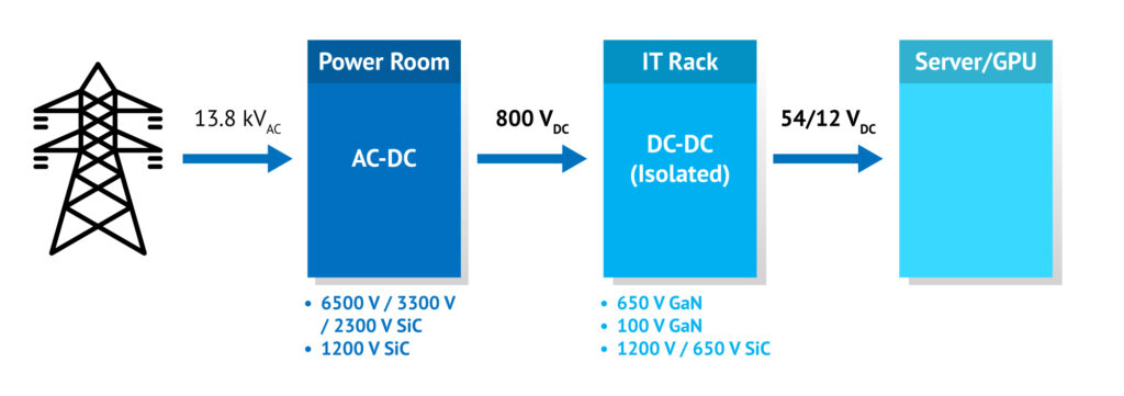
Fig. 1. Navitas GaN and SiC technologies cover the complete power delivery from grid to the GPU.
In August 2023, Navitas introduced a high-speed, high-efficiency 3.2 kW CRPS, achieving a 40% smaller size than best-in-class, legacy silicon solutions for power-hungry AI and Edge computing. This was followed by the world’s highest power density 4.5 kW CRPS, achieving a ground-breaking 137 W/in3, and an efficiency of over 97%. In November 2024, Navitas released the world’s first 8.5 kW AI data center power supply, powered by GaN and SiC that could meet 98% efficiency, complying with the Open Compute Project (OCP) and Open Rack v3 (ORv3) specifications. Additionally, Navitas created IntelliWeave, an innovative patented new digital control technique, that when combined with high-power GaNSafe and Gen 3-Fast SiC MOSFETs, enables PFC peak efficiencies to 99.3% and reduces power losses by 30% compared to existing solutions. Alongside the Computex exhibition in Taiwan, the latest release of their 12 kW PSU was presented at the Navitas ‘AI Tech Night’ on 21st May.
“We are proud to be selected by NVIDIA to collaborate on their 800 HVDC architecture initiative. Our latest innovations in high-power GaN and SiC technologies have seen world firsts and have created new inflections into markets such as AI datacenters and electric vehicles”, said Gene Sheridan, CEO and co-founder of Navitas. “With our wide portfolio range, we can support NVIDIA’s 800V HVDC infrastructure, from grid to the GPU. We appreciate that NVIDIA recognizes our technology and commitment to driving the next generation of data center power delivery.”
NVIDIA’s 800V HVDC architecture will improve end-to-end power efficiency up to 5%, reduce maintenance costs by 70% (due to fewer PSU failures), and lower cooling costs by directly connecting HVDC to the IT and compute racks.
Original – Navitas Semiconductor
-

Navitas Semiconductor has announced their latest 12 kW power supply unit (PSU) ‘designed for production’ reference design for hyperscale AI data centers with high-power rack densities of 120 kW.
The 12 kW PSU complies with Open Rack v3 (ORv3) specifications and Open Compute Project (OCP) guidelines. It utilizes Gen-3 Fast SiC MOSFETs, a novel ‘IntelliWeave™’ digital platform, and high-power GaNSafe ICs configured in 3-phase interleaved TP-PFC and FB-LLC topologies to ensure the highest efficiency and performance, with the lowest component count.
The 3-Phase interleaved totem-pole power factor correction (TP-PFC) is powered by Gen-3 Fast SiC MOSFETs with ‘trench-assisted planar’ technology, which has been enabled by over 20 years of SiC innovation leadership and offers world-leading performance over temperature, delivering cool-running, fast-switching, and superior robustness to support faster charging EVs and up to 3x more powerful AI data centers.
IntelliWeave digital control provides a hybrid control strategy of both Critical Conduction Mode (CrCM) and Continuous Conduction Mode (CCM), for light-load to full-load conditions, ensuring maximum efficiency while maintaining a simplistic design with low component count. This results in a 30% reduction in power losses compared to existing Continuous Conduction Mode (CCM) solutions.
The 3-phase interleaved full-bridge (FB) LLC topology is enabled by 4th generation high-power GaNSafe ICs, integrating control, drive, sensing, and critical protection features that allow unprecedented reliability and robustness. GaNSafe is the world’s safest GaN with short-circuit protection (350ns max latency), 2kV ESD protection on all pins, elimination of negative gate drive, and programmable slew rate control. All these features are controlled with four pins, allowing the package to be treated like a discrete GaN FET, requiring no VCC pin. Suitable for applications from 1 kW to 22 kW, 650 V GaNSafe in TOLL and TOLT packages are available with a range of RDS(ON)typ. from 18 to 70 mΩ.
The PSU is 790 x 73.5 x 40 mm and has an input voltage range of 180 – 305 VAC, outputting up to 50 VDC and delivering 12 kW when using input voltages above 207 VAC and 10 kW below this. Additionally, it implements active current sharing and over-current, over-voltage, under-voltage, and over-temperature protections. It has an operating temperature range of -5 to 45oC, a hold-up time of ³20 ms at 12 kW, and an inrush current of £3 times the steady-state current below 20 ms. Cooling is via the PSU’s internal fan.
“The continuation and leadership of Navitas’ AI power roadmap has seen a quadrupling in output power – from 2.7 to 12 kW – in just over 24 months,” said Gene Sheridan, CEO and co-founder of Navitas. “This increase in power delivery is vital for the world’s data centers to support the exponential power demanded by the latest GPU architectures. The ‘designed for production’ PSU enables our customers to quickly implement a highly efficient, simple, and cost-effective solution to address the power delivery challenges for AI and hyperscale data centers.”
The 12 kW PSU was presented at Navitas’ ‘AI Tech Night’ on 21st May, alongside the Computex exhibition in Taiwan.
Original – Navitas Semiconductor
-

Infineon Technologies AG is revolutionizing the power delivery architecture required for future AI data centers. In collaboration with NVIDIA, Infineon is developing the next generation of power systems based on a new architecture with central power generation of 800 V high-voltage direct current (HVDC).
The new system architecture significantly increases energy-efficient power distribution across the data center and allows power conversion directly at the AI chip (Graphic Processing Unit, GPU) within the server board. Infineon’s expertise in power conversion solutions from grid to core based on all relevant semiconductor materials silicon (Si), silicon carbide (SiC) and gallium nitride (GaN) is accelerating the roadmap to a full scale HVDC architecture.
This revolutionary step paves the way for the implementation of advanced power delivery architectures in accelerated computing data centers and will further enhance reliability and efficiency. As AI data centers already are going beyond 100,000 individual GPUs, the need for more efficient power delivery is becoming increasingly important. AI data centers will require power outputs of one megawatt (MW) and more per IT rack before the end of the decade. Therefore, the HVDC architecture coupled with high-density multiphase solutions will set a new standard for the industry, driving the development of high-quality components and power distribution systems.
“Infineon is driving innovation in artificial intelligence,” said Adam White, Division President Power & Sensor Systems at Infineon. “The combination of Infineon’s application and system know-how in powering AI from grid to core, combined with NVIDIA’s world-leading expertise in accelerated computing, paves the way for a new standard for power architecture in AI data centers to enable faster, more efficient and scalable AI infrastructure.”
“The new 800V HVDC system architecture delivers high reliability, energy-efficient power distribution across the data center,” said Gabriele Gorla, vice president of system engineering at NVIDIA. “Through this innovative approach, NVIDIA is able to optimize the energy consumption of our advanced AI infrastructure, which supports our commitment to sustainability while also delivering the performance and scalability required for the next generation of AI workloads.”
At present, the power supply in AI data centers is decentralized. This means that the AI chips are supplied with power by a large number of power supply units (PSU). The future system architecture will be centralized, making the best possible use of the constraint space in a server rack. This will increase the importance of leading-edge power semiconductor solutions using fewest power conversion stages and allowing upgrades to even higher distribution voltages.
Infineon is a leader in power semiconductor solutions and systems integration. The company expects the proportion of power semiconductors in a centralized HVDC architecture to be similar or higher than in today’s AC distribution architecture. Additionally, to the scaling of the HVDC power architecture, Infineon continues to support state of the art DCDC multiphase solutions and intermediate architectures for hyperscalers and AI data center operators with a broad product portfolio based on all relevant semiconductor materials along the entire power flow.
Learn more about Infineon’s AI power and data center solutions here.
Original – Infineon Technologies
-
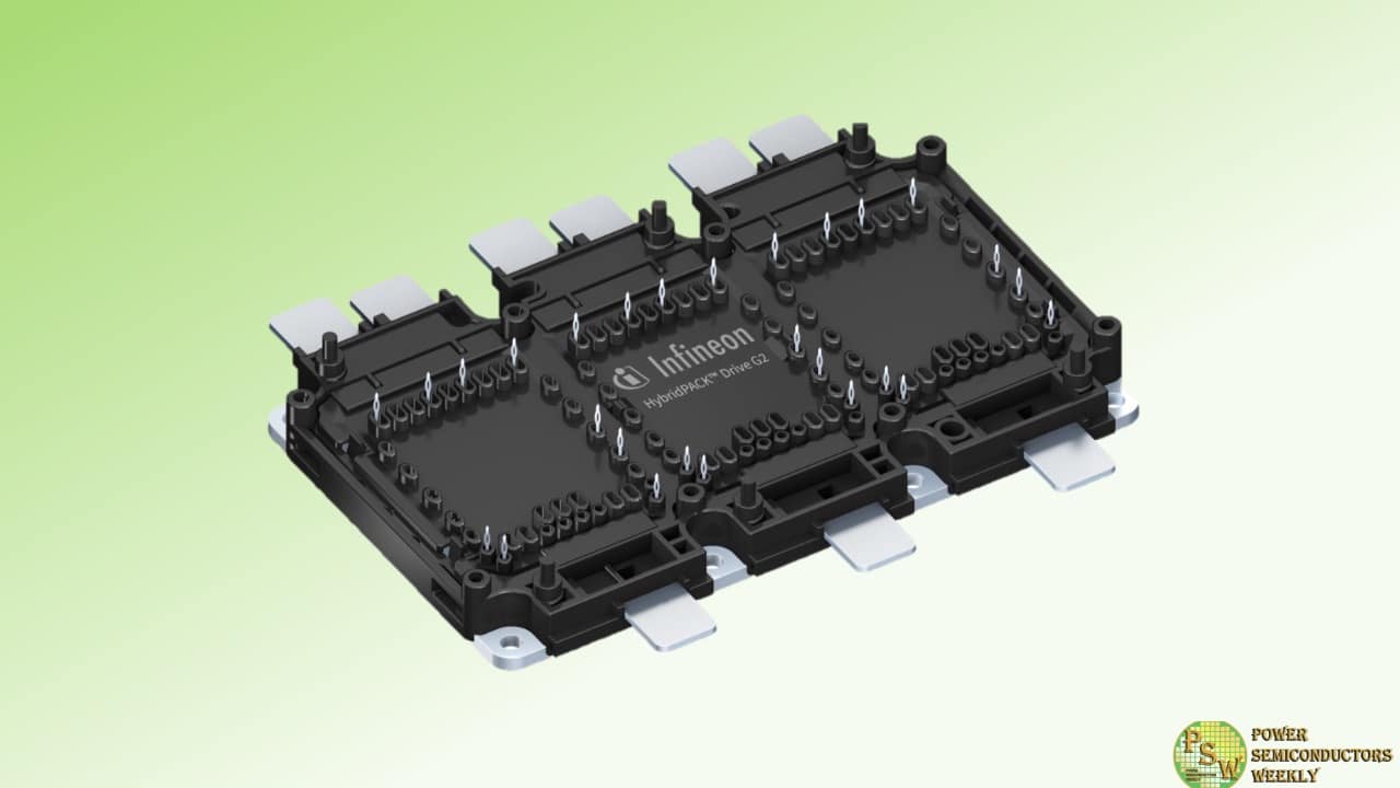
Infineon Technologies AG will supply Rivian’s R2 platform with power modules for traction inverters. The R2 platform will use silicon carbide (SiC) and silicon (Si) modules from Infineon’s HybridPACK™ Drive G2 family. Supply is expected to start in 2026. Additionally, Infineon will supply other products for the platform, including AURIX™ TC3x microcontrollers and power management ICs.
“We are committed to enhancing the performance and range of electric vehicles jointly with innovative automotive companies like Rivian,” said Stefan Obersriebnig, head of the product line for high voltage modules in Infineon’s Automotive Division. “Our dedication for innovation and zero-defect quality has made us the preferred partner of the automotive industry. With our broad product portfolio, system expertise and manufacturing capabilities, we are a key enabler of emission-free, sustainable mobility.”
HybridPACK Drive is Infineon’s market-leading power module family for electric vehicles. With more than 10.5 million units sold since 2017, it contributes significantly to the transition to electromobility. This transition will lead to strong market growth for power semiconductors, especially those based on wide bandgap materials like SiC.
With the expansion of its Kulim fab, Infineon is building the world’s most competitive 200-millimeter SiC power fab and further strengthens its market-leading role as a high-quality, high-volume supplier to the automotive industry. As “Infineon One Virtual Fab” for highly innovative wide bandgap (WBG) technologies, Infineon’s production sites in Kulim and Villach share technologies and processes. This allows for fast ramping and smooth and highly efficient operations in SiC and gallium nitride (GaN) manufacturing and reinforces Infineon’s technological leadership across the spectrum of all power semiconductor materials, in silicon as well as SiC and GaN.
Original – Infineon Technologies
-

Infineon Technologies AG has introduced the CoolGaN™ bidirectional switch (BDS) 650 V G5, a gallium nitride (GaN) switch capable of actively blocking voltage and current in both directions. Featuring a common-drain design and a double-gate structure, it leverages Infineon’s robust gate injection transistor (GIT) technology to deliver a monolithic bidirectional switch, enabled by Infineon’s CoolGaN technology. The device serves as a highly efficient replacement for traditional back-to-back configurations commonly used in converters.
The bidirectional CoolGaN switch offers several key advantages for power conversion systems. By integrating two switches in a single device, it simplifies the design of cycloconverter topologies, enabling single-stage power conversion, eliminating the need for multiple conversion stages. This leads to improved efficiency, increased reliability, and a more compact design. BDS-based microinverters also benefit from higher power density and reduced component count, which simplifies manufacturing and reduces costs. Additionally, the device supports advanced grid functions such as reactive power compensation and bidirectional operation.
As a result, this solution holds significant potential across a wide range of applications, including:
Microinverters: The CoolGaN bidirectional switch enables simpler and more efficient microinverter designs, reducing both size and cost. This makes microinverters more attractive for residential and commercial solar installations.
Energy Storage Systems (ESS): In ESS applications such as battery chargers and dischargers, the switch allows for more efficient and reliable energy storage and release.
Electric Vehicle (EV) Charging: In EV charging systems, the BDS switch supports faster, more efficient charging while also enabling vehicle-to-grid (V2G) functionality, where energy stored in the vehicle battery can be fed back into the grid.
Motor control: The CoolGaN BDS is ideal for use in Current Source Inverters (CSI) for industrial motor drives. Compared to traditional Voltage Source Inverters (VSI), CSIs offer benefits such as:
- Producing a sinusoidal output voltage, which supports longer cable runs, reduced losses, and improved fault tolerance.
- Replacing the DC-link capacitor with an inductor, improving high-temperature performance and short-circuit protection.
- Higher efficiency at partial loads, lower EMI, inherent buck-boost capability for voltage variation, and scalability for parallel operation.
These features make CSIs a more robust and efficient alternative for industrial motor applications.
AI data centers: In AI server power supplies, bidirectional switches like CoolGaN support higher switching frequencies and power density in architectures such as Vienna rectifiers and H4 PFCs. A single CoolGaN BDS can replace two conventional switches, reducing component count, cost, size, and overall power losses.
The CoolGaN bidirectional switch (BDS) 650 V G5 is available for ordering now as well as samples of the 110 mΩ product. More information is available here.
Original – Infineon Technologies
-

To enable the next generation of solid-state power distribution systems, Infineon Technologies AG is expanding its silicon carbide (SiC) portfolio with the new CoolSiC™ JFET product family. The new devices deliver minimized conduction losses, solid turn-off capability, and high robustness, making them ideal for advanced solid-state protection and distribution.
With robust short-circuit capability, thermal stability in linear mode, and precise overvoltage control, CoolSiC JFETs enable reliable and efficient system performance in a wide range of industrial and automotive applications, including solid-state circuit breakers (SSCBs), AI data center hot-swaps, eFuses, motor soft starters, industrial safety relays, and automotive battery disconnect switches.
“With CoolSiC JFET, we are addressing the growing demand for smarter, faster, and more robust power distribution systems,” says Dr. Peter Wawer, Division President Green Industrial Power at Infineon Technologies. “This application-driven power semiconductor technology is specifically designed to provide our customers with the tools they need to solve the complex challenges in this rapidly evolving space. We are proud to introduce devices that achieve best-in-class R DS(ON), setting a new standard for SiC performance and reaffirming Infineon’s leadership in the field of wide-bandgap technology.”
The first generation of CoolSiC JFETs features ultra-low R DS(ON) starting at 1.5 mΩ (750 V BDss) and 2.3 mΩ (1200 V BDss), significantly reducing conduction losses. The bulk-channel optimized SiC JFET offers high robustness under short-circuit and avalanche failure conditions. Housed in a Q-DPAK top-side cooled package, the devices support easy paralleling and scalable current handling, enabling compact, high-power systems with flexible layout and integration options. Their predictable switching behavior under thermal stress, overload and fault conditions provides maximum long-term reliability in continuous operation.
To meet the thermal and mechanical challenges of harsh application environments, CoolSiC JFETs leverage Infineon’s advanced .XT interconnection technology with diffusion soldering. This significantly improves transient thermal impedance and robustness under pulsed and cyclic loads typical of industrial power systems. Tested and qualified under real-world operating conditions of solid-state power switches and based on the industry-standard Q-DPAK package, the devices enable quick and seamless design integration in both industrial and automotive applications.
Engineering samples of the new CoolSiC JFET family will be available later in 2025, with volume production starting in 2026. The product portfolio will be further expanded with a variety of packages and modules. The product family has been successfully demonstrated at the Infineon booth at PCIM Europe 2025 in Nuremberg. More information is available at www.infineon.com/jfet.
Original – Infineon Technologies
-

DENSO CORPORATION and ROHM Co., Ltd. announced that the two companies have reached a basic agreement to establish a strategic partnership in the semiconductor field. This agreement follows discussions and considerations that began in September 2024.
Recently, the importance of semiconductors that support the electrification and intelligence of vehicles has been increasing significantly. This is driven by the development and spread of electric vehicles aimed at achieving carbon neutrality, as well as the realization of automated driving, which is expected to contribute to zero fatalities in traffic accidents.
DENSO and ROHM have a long-standing collaboration in the trade and development of automotive semiconductors. Going forward, both companies will integrate DENSO’s advanced system construction capabilities in the automotive sector with ROHM’s cutting-edge semiconductor technology, cultivated in the consumer market. This partnership will focus on enhancing the lineup of high-quality devices, particularly analog ICs, that support vehicle electrification and intelligence, and deepening collaboration in development. Additionally, in highly compatible fields within their semiconductor businesses, both companies will discuss broad collaboration. By globally supplying products created through this co-creation, both companies aim to contribute to technological innovation in the automotive field and realize a sustainable mobility society.
To further solidify this partnership, DENSO and ROHM will continue to consider strengthening their capital relationship.
DENSO CORPORATION President & CEO, Shinnosuke Hayashi
DENSO positions semiconductors as key devices to realize next-generation vehicle systems and has been deepening its cooperative relationships with semiconductor manufacturers that possess rich experience and knowledge. ROHM has a wide range of semiconductor lineups that are crucial for automotive electronics products, essential for vehicle intelligence and electrification. We are very pleased that the partnership with ROHM is progressing smoothly. By further deepening the collaboration between both companies and integrating DENSO’s accumulated automotive technology and expertise, we believe we can contribute to the development of the mobility society through stable supply and enhanced product value.ROHM Co., Ltd. President (Representative Director), Katsumi Azuma
We are very pleased to deepen our collaborative relationship with DENSO, a leader in technological innovation for the mobility society. This partnership not only strengthens our relationship as suppliers but also envisions broad collaboration in the semiconductor business of both companies. Initially, we will focus on the development of analog ICs related to next-generation systems such as electrification, automated driving, and connected vehicles. Furthermore, without narrowing the scope, we will integrate our respective technologies, knowledge, and assets across a wide range of fields to contribute to technological innovation and stable supply in the automotive industry.Original – DENSO
