-

A pan-European consortium dedicated to developing sustainable processes and technologies for the semiconductor-manufacturing industry today announced the launch of the GENESIS project. This integrated, large-scale initiative aims to enable Europe’s chip industry to meet its sustainability goals—from materials development to final waste treatment.
Coordinated by CEA-Leti, the three-year project brings together 58 partners spanning the entire European semiconductor value chain, from large enterprises and SMEs to research institutes, universities, and industry associations. GENESIS will drive innovative solutions in emission control, eco-friendly materials such as alternatives to PFAS-based ones, waste minimization, and raw material reuse, directly aligned with the European Green Deal and European Chips Act.
“GENESIS is designed to address the complex challenges of building a truly sustainable semiconductor ecosystem,” said Laurent Pain, Sustainable Electronics Program director at CEA-Leti. “Its structure reflects both the urgency and the opportunity of Europe’s green transition, powered by the complementary expertise and close collaboration of its partners.”
Pain, manager of the project, noted that the team expects to deliver approximately 45 sustainability-driven innovations covering the semiconductor lifecycle, guided by four strategic pillars that form the technological foundation of GENESIS’s vision for a green European semiconductor industry:
- Pillar 1 – Monitoring & Sensing: Real-time emissions tracking, traceability, and process feedback systems,
- Pillar 2 – New Materials: PFAS-free chemistries and low-GWP alternatives for advanced semiconductor processes,
- Pillar 3 – Waste Minimization: Innovations in recycling (solvent, gas, slurries), reuse, and sustainable replacements, and
- Pillar 4 – Critical Raw Materials Mitigation: Strategies to reduce dependency on CRM and strengthen resource security.
Complimenting these pillars, the project’s objectives establish an overall framework that includes deploying sensor-integrated abatement systems to reduce PFAS and GHG emissions. It also aims to position Europe as a leader in green semiconductor innovation by aligning supply-chain practices with environmental regulations.
“The launch of the GENESIS project marks a critical step toward aligning Europe’s semiconductor ambitions with its climate commitments,” said Anton Chichkov, head of programs at Chips Joint Undertaking (Chips JU), a public-private partnership created to bolster Europe’s semiconductor industry by fostering collaboration between the EU, member states, and the private sector.
“As chips become the backbone of everything from AI to energy systems, their environmental footprint is rapidly growing,” he said. “GENESIS responds to this urgent challenge by pioneering sustainable alternatives in materials, waste reduction, and resource efficiency. Through this initiative, Europe is not only investing in cleaner technologies—it’s positioning itself as a global leader in green semiconductor manufacturing.”
With a budget of close to €55 million, the GENESIS project is co-funded through the Chips Joint Undertaking by the European Commission, participating EU member states, and the Swiss State Secretariat for Education, Research and Innovation (SERI).
Original – CEA-Leti
-

Reflex Drive, a deep tech startup from India has selected power devices from Infineon Technologies AG for its next-generation motor control solutions for unmanned aerial vehicles (UAVs). By integrating Infineon’s OptiMOS™ 80 V and 100 V , Reflex Drive’s electric speed controllers (ESCs) achieve improved thermal management and higher efficiency, enabling high power density in a compact footprint.
Additionally, the use of Infineon’s MOTIX™ IMD701 controller solution – which combines the XMC1404 microcontroller with the MOTIX 6EDL7141 3-phase gate driver IC – delivers compact, precise, and reliable motor control. This enables improved performance, greater reliability, and longer flight times for UAVs.
“Our partnership with Reflex Drive is an important contribution to our market launch strategy and presence in India,” says Nenad Belancic, Global Application Manager Robotics and Drones at Infineon. “Our partner has proven its expertise with numerous customers who have obtained aviation certifications. In addition, the company has presented its innovative technologies enabled by Infineon systems at important international industry events.”
“Our collaboration with Infineon has led to significant advances in UAV electronics,” says Amrit Singh, Founder of Reflex Drive. “We believe drones have the potential to transform industries, from agriculture to logistics, and with Infineon’s devices, we can help drive this transformation at the forefront.”
Reflex Drives’s ESCs with field-oriented control (FOC) offer improved motor efficiency and precise control, while its high-performance BLDC motors are designed for optimized flight control and enable predictive maintenance of drive systems. Weighing only 180 g and with a compact volume of 120 cm³, the ESCs can deliver continuous power output of 3.8 kW (12S/48 V, 80 A continuous).
Due to their lightweight design, robust power output, and consistent FOC control – even under demanding weather conditions – make them ideal for motors in the thrust range from 15 to 20 kg. Therefore, they are particularly suitable for drone applications in the fields of agricultural spraying technology, seed dispersal, small-scale logistics, and goods transport.
Original – Infineon Technologies
-

Magnachip Semiconductor Corporation announced that the Board of Directors of the Company has approved an initiative intended to enhance independent Board oversight and feedback to management in conjunction with the Company’s previously announced transition to a pure-play Power business, implementation of management’s 3-3-3 strategy, and launch of new-generation Power discrete products.
The 3-3-3 strategy aims for Magnachip to achieve $300 million in annual revenue and a 30% gross margin over a three-year horizon to align Magnachip’s product roadmap, R&D investments, and operational priorities to drive structural improvements and sustainable profitability.
The Company’s Chairman, Camillo Martino, has agreed, on behalf of the Board to spend additional time on-site at the Company’s headquarters in Korea to meet with management and report back to the full Board during the implementation phase of its 3-3-3 strategy to achieve profitable growth and to maximize shareholder value. The Board expects Mr. Martino to spend several days each month in Korea for at least the remainder of 2025 in order to more closely oversee and report regularly to the Board’s other independent directors on the Company’s progress in its important strategy milestones, as well as to provide more timely feedback to management on behalf of the Board.
Camillo Martino, Chairman of Magnachip, said, “I look forward to spending more time on the ground with our management team in Korea to assist the full Board in its oversight responsibilities during the Company’s implementation of its 3-3-3 strategy as a pure-play Power business. Spending additional time on-site with the management team will allow more streamlined and timely communication with the rest of the independent Board members as Magnachip management implements its strategy to deliver new-generation Power discrete and Power IC products while also achieving its financial targets.”
YJ Kim, Magnachip’s CEO, said, “We welcome the additional support from Camillo on behalf of the Board, and look forward to continuing to provide timely feedback to the rest of the Board as we pursue these new exciting opportunities for Magnachip.”
Original – Magnachip Semiconductor
-

GlobalFoundries announced plans to invest $16 billion to expand its semiconductor manufacturing and advanced packaging capabilities across its facilities in New York and Vermont. GF’s investment is a strategic response to the explosive growth in artificial intelligence, which is accelerating demand for next-generation semiconductors designed for power efficiency and high-bandwidth performance across datacenters, communications infrastructure and AI-enabled devices.
GF is collaborating with major technology companies such as Apple, SpaceX, AMD, Qualcomm Technologies, Inc., NXP and GM, that are committed to reshoring semiconductor production to the U.S. and diversifying their global supply chains. These companies partner with GF to support their production of U.S.-made chips, underscoring GF’s role as a trusted supplier of essential semiconductors and a key enabler of supply chain security.
“At GlobalFoundries, we are proud to partner with pioneering technology leaders to manufacture their chips in the United States—advancing innovation while strengthening economic and supply chain resiliency,” said Tim Breen, CEO of GlobalFoundries. “The AI revolution is driving strong, durable demand for GF’s technologies that enable tomorrow’s datacenters – including GF’s leading silicon photonics, as well as GaN for power applications. Meanwhile at the edge, GF’s proprietary FDX technology is uniquely positioned to support AI functionality with low power consumption. With all these technologies and more manufactured right here in the U.S., GF is proud to play its part in accelerating America’s semiconductor leadership.”
“GlobalFoundries investment is a great example of the return of United States manufacturing for critical semiconductors,” said U.S. Secretary of Commerce, Howard Lutnick. “President Trump has made it a fundamental objective to bring semiconductor manufacturing home to America. Our partnership with GlobalFoundries will secure U.S. semiconductor foundry capacity and technology capabilities for future generations.”
The rapid rise of AI in both the cloud and at the edge is driving the adoption of new technology platforms and 3D heterogeneous integration technologies. These advanced solutions are essential to meet the exponentially growing requirements for power efficiency, bandwidth density and performance. GF is uniquely positioned to lead in this space, with its 22FDX® and silicon photonics capabilities in production in New York and advanced development of differentiated GaN-based power solutions in Vermont.
GF’s investment builds upon the company’s existing U.S. expansion plans, including more than $13 billion to expand and modernize its New York and Vermont facilities and funding for its recently launched New York Advanced Packaging and Photonics Center—the first U.S.-based facility of its kind dedicated to silicon photonics packaging. GF is committing an additional $3 billion, which includes advanced research and development initiatives focused on packaging innovation, silicon photonics and next-generation GaN technologies. In aggregate, these investments represent a $16 billion plan to strengthen U.S. semiconductor leadership and accelerate innovation in AI, aerospace, automotive and high-performance communications.
“Today’s announcement is a direct result of President Trump’s leadership and his vision to bring back high-paying manufacturing jobs and reestablish secure, domestic supply chains for critical technologies,” said Dr. Thomas Caulfield, Executive Chairman of GlobalFoundries. “We look forward to continuing to work with the U.S. government to help create the conditions for industry and government to work together and drive meaningful, long-term impact.”
“GlobalFoundries has supplied semiconductors for Apple products since 2010 and we’re excited to see them expand right here in the United States. These chips are an essential part of Apple products like iPhone, and they’re a powerful example of American manufacturing leadership.”
Tim Cook, Apple’s CEO
“Advanced semiconductors are critical to the advanced satellite capabilities which SpaceX has been pioneering for over two decades. We are excited by the expansion of GlobalFoundries’ manufacturing base right here in the U.S., which is core to Starlink’s growth and our commitment to manufacturing in the U.S., as well as our mission to deliver high-speed internet access to millions of people around the world.”
Gwynne Shotwell, president and COO at SpaceX
“As a valued technology partner, we’re pleased to see GlobalFoundries deepen its commitment to U.S. manufacturing. These efforts are critical to building a secure and resilient semiconductor supply chain in the U.S. to support the next wave of innovation in our industry.”
Dr. Lisa Su, AMD Chair and CEO
“As a strategic supplier of Qualcomm, GlobalFoundries shares our vision for strengthening U.S. chip production capacity. This commitment from GlobalFoundries will help secure a resilient semiconductor supply chain to support the next wave of U.S. technology innovation, especially in areas vital to enabling power efficient computing, connectivity, and edge intelligence.”
Cristiano Amon, president and CEO of Qualcomm Incorporated
“Deepening our partnership with GlobalFoundries aligns with NXP’s hybrid manufacturing strategy, where we work with leading foundry partners to better serve our customers’ strategic technology, capacity and resilience needs. This collaboration allows us to scale efficiently, expand production in the U.S. and continue delivering for our customers. It’s a strong step forward in building a resilient, high-performing semiconductor supply chain in the United States.”
Kurt Sievers, chief executive officer of NXP Semiconductors
“Semiconductors are critical to the future of vehicles, and their importance will only grow. GlobalFoundries’ investment supports our work to secure a reliable, U.S.-based chip supply—essential for delivering the safety, infotainment and features our customers expect.”
Mark Reuss, president of General Motors
Original – GlobalFoundries
-

Navitas Semiconductor announced its partnership with BrightLoop supporting their latest series of hydrogen fuel-cell chargers with automotive qualified Gen 3 ‘Fast’ SiC (G3F) MOSFETs for heavy-duty agricultural transportation equipment.
BrightLoop offers leading-edge, top-performance solutions with power conversion efficiencies over 98% and extreme power densities up to 35 kW/kg and 60 kW/L. Their high-voltage, high-power multiverters paired to BrightLoop’s Power Flow Processor technology are designed to deliver exceptional performance in both AC and DC applications, such as energy management scenarios for fuel cells and heavy-duty applications, as well as HV network adaptation.
Navitas’ auto-qualified G3F SiC MOSFETs are incorporated into BrightLoop’s 250 kW HV-DC/DC converter, with an output of 950VDC at 480A, and can be paralleled to achieve megawatt power capability.
Enabled by 20 years of SiC innovation leadership, GeneSiC proprietary ‘trench-assisted planar’ technology provides world-leading performance over temperature, delivering high-speed, cool-running operation for high-power, high-reliability applications. G3F SiC MOSFETs deliver high-efficiency with high-speed performance, enabling up to 25°C lower case temperature, and up to 3x longer life than SiC products from other vendors.
Trench-assisted planar technology enables an extremely low RDS(ON) increase versus temperature, which results in the lowest power losses across the complete operating range and offers up to 20% lower RDS(ON) under real-life operation at high temperatures compared to competition. All GeneSiC MOSFETs have the highest-published 100%-tested avalanche capability, 30% longer short-circuit withstand time, and tight threshold voltage distributions for easy paralleling.
“We are proud to partner with BrightLoop, the established leaders in leading-edge high-power density and efficiency converters,” said Gene Sheridan, CEO and co-founder of Navitas. “Both companies provide the technology and system leadership to enable the roadmap for next generation, high-power density, high-reliability converter solutions”.
“Navitas offers leading-edge SiC technology where efficiency, ruggedness, and reliability are paramount. Our high power-density, smart, efficient, and scalable multiverters lead the industry by enhancing the quantity and quality of energy delivered to our customers”, said Florent Liffran, CEO and founder of BrightLoop.
Original – Navitas Semiconductor
-

Infineon Technologies AG announced the first of a new family of radiation hardened Gallium Nitride (GaN) transistors, fabricated at Infineon’s own foundry, based on its proven CoolGan™ technology. Designed to operate in harsh space environments, the company’s new product is the first in-house manufactured GaN transistor to earn the highest quality certification of reliability assigned by the United States Defense Logistics Agency (DLA) to the Joint Army Navy Space (JANS) Specification MIL-PRF-19500/794.
The new radiation hardened GaN High Electron Mobility Transistor (HEMT) devices are engineered for mission-critical applications required in on-orbit space vehicles, manned space exploration, and deep space probes. Combining the robust performance of GaN HEMTs with Infineon 50+ years of experience in high reliability applications, the new power transistors deliver best-in-class efficiency, thermal management and power density for smaller, lighter, and more reliable space designs. The devices complement Infineon’s proven legacy radiation hardened silicon MOSFET portfolio, providing customers with access to a full catalog of power solutions for space applications.
“The Infineon team continues to push the limits of power design with our new GaN transistor line,” said Chris Opoczynski, Senior Vice President and General Manager HiRel, at Infineon. “This milestone brings the next-generation of high reliability power solutions for mission-critical defense and space applications that utilize the superior material properties of wide bandgap semiconductors to customers serving the growing aerospace market.”
The first three product variations in the new radiation hardened GaN transistor line are 100 V, 52 A devices featuring an industry leading (R DS(on) (drain source on resistance) of 4 mΩ (typical) and total gate charge (Qg) of 8.8 nC (typical). Encased in robust hermetically sealed ceramic surface mount packages, the transistors are Single Event Effect (SEE) hardened up to LET (GaN) = 70 MeV.cm2/mg (Au ion). Two devices, which are not JANS certified, are screened to a Total Ionizing Dose (TID) of 100 krad and 500 krad. The third device, screened to 500 krad TID, is qualified to the rigorous JANS Specification MIL-PRF-19500/794.
Infineon is the first company in the industry to achieve the DLA JANS certification for fully internally manufactured GaN power devices. DLA JANS certification requires rigorous levels of screening and Quality of Service Class Identifiers to ensure the performance, quality, and reliability required for space flight applications – making Infineon a leader in GaN for high reliability applications. Infineon is also running multiple lots prior to full JANS production release to ensure long term manufacturing reliability.
Engineering samples and evaluation boards are available immediately with the final JANS device being released in the summer of 2025. Additional JANS parts are launching soon, expanding available voltages and currents to enable customers greater flexibility in creating efficient and reliable designs. For more information, visit www.infineon.com/radhardgan
Original – Infineon Technologies
-
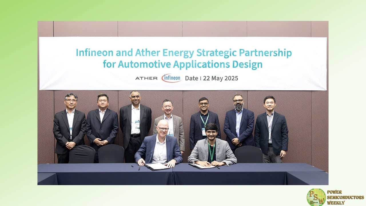
Ather Energy, a leading electric two-wheeler manufacturer in India and Infineon Technologies Asia Pacific Pte Ltd, a global leader in semiconductor solutions, signed a Memorandum of Understanding (MoU) in Seoul, South Korea, to jointly drive innovation in the electric vehicle (EV) industry in India. The collaboration focuses on advancing semiconductor technologies to support light electric vehicles (LEVs), charging infrastructure, and safety, with a shared vision to contribute to India’s growing EV ecosystem.
The partnership aims to leverage cutting-edge semiconductor solutions from Infineon based on various technologies, microcontrollers and automotive related sensors, alongside Ather’s expertise in designing state-of-the-art LEVs (Light Electric Vehicles). Together, the companies will work towards enabling more efficient, reliable, and cost-effective EV solutions, driving the adoption of electric two-wheelers in India.
Speaking on the occasion, Swapnil Jain, Executive Director and CTO, Ather Energy, said: “At Ather, we’ve always believed that building great EVs starts with getting the fundamentals right – performance, efficiency, reliability. Our approach has always been grounded in first-principles thinking and deep engineering, questioning how every system can be made better, faster, and more efficient. That’s where semiconductor innovation becomes critical. Infineon’s leadership in semiconductors and system solutions brings deep expertise that aligns with our engineering-first approach. Our partnership with Infineon gives us access to advanced technologies that can help us improve key systems, from charging to safety and explore ways to reduce system complexity and cost. We’re looking forward to seeing how this collaboration can help us push the boundaries, not just for our products, but for the larger EV ecosystem in India.”
Highlighting the importance of this partnership, Peter Schaefer, Executive Vice President and Chief Sales Officer Automotive at Infineon, said: “India is one of the fastest-growing EV markets globally, and electric two-wheelers are at the heart of this transformation. We are thrilled to partner with Ather Energy to enable the next generation of sustainable mobility solutions. Our advanced SiC and GaN technologies will help drive energy-efficient and high-performance electric vehicles. This partnership will foster innovation that contributes meaningfully to India’s ambitious objective to reach a 30 percent sales share for EVs by 2030.”
This collaboration will explore sensing and safety innovations to elevate vehicle safety and user experience. These solutions deliver significant advantages in terms of energy efficiency, charging speed, and overall system reliability, making EVs more accessible, sustainable, convenient and appealing to consumers.
Original – Infineon Technologies
-

MCC introduced the 100V P-channel MOSFET that optimizes space without sacrificing performance. Housed in a compact DFN3333 package, MCG085P10 utilizes innovative trench power LV MOSFET technology to maximize reliability and efficiency.
From its exceptionally low 85mΩ on-resistance that reduces voltage drops and heat generation to low conduction losses, this component is well-suited for diverse applications. Requiring lower gate drive voltages, our MOSFET ensures stable operation under harsh working conditions.
MCG085P10 also solves common challenges, including efficiency, heat management, and space constraints, offering engineers an edge in modern electronic design.
Features & Benefits:
- Trench Power LV MOSFET Technology: Enhances performance with reduced gate drive requirements and improved efficiency.
- Low On-Resistance: Boosts overall efficiency thanks to minimal voltage drop and heat generation during operation.
- Low Conduction Losses: Increases energy savings and improves thermal performance in power applications.
- Compact DFN3333 Package: Enables smaller, more innovative electronic designs.
Original – Micro Commercial Components
-

On May 15, GlobalWafers Co., Ltd. hosted U.S. Investment Accelerator Executive Director Michael Grimes, Taiwan Minister of Economic Affairs Kuo Jyh-huei, AIT Director Raymond Greene, ROC Taiwan’s Representative to the United States Alexander Yui, Sherman Mayor Shawn Teamann, and hundreds of customers, suppliers, and partners in Sherman, Texas to celebrate the Grand Opening of GlobalWafers America (GWA), the company’s newest and most advanced 300mm silicon wafer manufacturing facility.
GlobalWafers made the decision to build its flagship facility in the United States in May 2022 and held the groundbreaking ceremony in Sherman on December 2, 2022. To date, the US$3.5 billion project has created 1200 construction and 180 permanent jobs in North Texas and will employ up to 650 engineering, technical and operational professionals by the end of 2028.
During the celebration Chairperson Doris Hsu unexpectedly announced the company’s plan to further grow its U.S. manufacturing base, stating: “On the three-year anniversary of our decision to build GWA, I am pleased to announce GlobalWafers’ intention to expand our current U.S. investment by another $4 billion to reach $7.5 billion!” In alignment with growth in market demand- combined with an advantageous tariff structure favoring cost effective U.S. expansion- GlobalWafers expects to add phases 3 and 4 to its existing commitment in Sherman. As the only advanced wafer supplier manufacturing in the United States, this additional investment, bolstered by ongoing support from the U.S. Government and the Trump Administration, is expected to fully secure the advanced wafer supply needed to power a broad range of next-generation technologies and innovation.
On this point, GWC President Mark England noted: “GWA will fill a key vulnerability in the U.S. supply chain and help build a more complete and self-sufficient local semiconductor ecosystem — one that is more resilient and future-ready.” In fact, GWA is the only fully integrated advanced silicon wafer manufacturing facility participating in the U.S. Government’s CHIPS for America Program and is the first production line of its kind built in the United States in over 20 years.
Under the CHIPS Program- now part of President Trump’s new U.S. Investment Accelerator- the U.S. Department of Commerce is investing US$406 million in GlobalWafers’ new U.S. operations in a strategy to rebuild a key node of the U.S. semiconductor supply chain. At the event, U.S. Investment Accelerator Executive Director Michael Grimes observed: “GlobalWafers investment is a great example of the return of United States manufacturing in a critical industry. President Trump and Secretary Lutnick have made it a fundamental objective to bring semiconductor manufacturing home to America. Through our work with GWA, we are ensuring that the essential starting material for advanced chips is manufactured right here in United States. GlobalWafers current investment, together with its new commitment announced today, will secure U.S. wafer supply for generations to come.”
The City of Sherman, Grayson County, and the State of Texas have also provided important incentives in the form of land, direct grants, tax incentives and excellent manufacturing infrastructure. Chairperson Doris Hsu noted, “There is simply not a more welcoming location in all the United States for doing business than Texas, Grayson County and Sherman. They have worked strategically to build the Silicon Prairie and GWA is thrilled to be part of it.” Governor Greg Abbott remarked, “We are proud that GlobalWafers America is now calling Texas home. GWA is rounding out the already well-established Texas semiconductor ecosystem, setting Texas apart as the only state in the country with advanced silicon wafers.”
From construction to production, GlobalWafers has partnered with hundreds of best-in-class suppliers who have also brought advanced engineering systems, technology and business processes to the project. “Without construction partners, toolmakers and materials suppliers also pushing the edge of their capabilities, GWA would not be able to deliver the quality wafers our customers have come to expect from GlobalWafers,” said GWA VP of Operations Wyatt Watson. “The GWA project has brought out the best of our entire supply chain.”
GlobalWafers is one of five global suppliers of advanced semiconductor wafers and the only one expanding in the United States during this new era of supply chain regionalization. Along these lines, Ashlie Wallace, GlobalFoundries’ SVP of Global Supply Chain, echoed the sentiment of many customers noting, “As a longstanding strategic partner, we are pleased to see GlobalWafers increasing domestic supply of silicon wafers critical to the essential semiconductors we manufacture.”
300mm silicon wafers are the essential input used by foundries and integrated device manufacturers to produce leading-edge, mature-node, and memory chips. Silicon from GWC’s semiconductor wafers is found in essentially every device that powers modern life– from home appliances, automobiles and physical infrastructure to cell phones, computers, and AI applications.
Further to the strategic phase 3 & 4 expansion announced today, GWA’s new 142-acre campus in Sherman— designed to accommodate up to six phases — has space to add two additional phases and significantly grow capacity in lockstep with chip producers who have collectively announced over US$500 billion in new U.S. investments over the next decade.
As part of our core ESG commitment, GlobalWafers companies worldwide practice green manufacturing. Once fully ramped, GWA will run on 100% renewable energy to produce the world’s most advanced silicon wafers. Across the GlobalWafers family, we remain deeply committed to minimizing our environmental impact while enabling the next generation of semiconductor innovation.
GlobalWafers Co., Ltd., the world’s third largest supplier of semiconductor wafers, maintains 18 manufacturing and operational sites spanning three continents and nine countries. The company is one of the global leaders in semiconductor technology, providing innovative and advanced technology solutions to leading chip manufacturers to transform lives around the world.
Original – GlobalWafers
-

Soitec announced the appointment of Albin Jacquemont as its new Chief Financial Officer (CFO).
Albin Jacquemont brings over 30 years of international experience in financial leadership, strategic planning, and corporate governance. His career spans listed and private equity-backed industrial and technology companies, including Inetum, Saur, Altran Technologies, Darty, and Carrefour. Throughout his tenure in these organizations, he has led major financial transformations and delivered significant value through operational performance improvement, cash-flow optimization and M&A execution.
In his new role, Albin Jacquemont will be responsible for all finance-related matters at Group level. He will play a pivotal role in reinforcing Soitec’s financial and operational foundations and supporting the company’s next phase of sustainable growth and value creation.
He succeeds Léa Alzingre, who will be stepping down to pursue new professional opportunities, having supported Soitec’s growth over the past six years.
“We are delighted to welcome Albin Jacquemont to Soitec’s Executive Committee. His extensive experience across complex industrial and technology environments, combined with his proven track record in financial transformation and value creation, will be instrumental as we continue to scale globally. I am confident that his leadership will strengthen our financial strategy and support the acceleration of our sustainable growth ambitions. I would also like to warmly thank Léa Alzingre for her strong commitment and valuable contributions to Soitec’s development during her tenure”, commented Pierre Barnabé, Soitec’s CEO.
“I am honored and excited to join Soitec’s Executive Committee, a global leader in innovative semiconductor materials. After a career spanning over three decades in senior financial leadership roles across Europe, the U.S., and emerging markets — including listed groups and private equity-owned companies — I look forward to bringing my experience to support Soitec’s global ambitions and pioneering technologies”, Albin Jacquemont stated.
Original – Soitec
