-
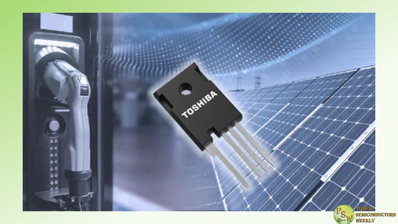
Toshiba Electronic Devices & Storage Corporation has launched silicon carbide (SiC) MOSFETs, the “TWxxxZxxxC series,” that use a four-pin TO-247-4L(X) package that reduces switching loss with the company’s latest 3rd generation SiC MOSFETs chip for industrial equipment. Volume shipments of ten products, five with 650V ratings and five with 1200V, start today.
The new products are the first in Toshiba’s SiC MOSFET line-up to use the four-pin TO-247-4L(X) package, which allows Kelvin connection of the signal source terminal for the gate drive. The package can reduce the effect of source wire inductance inside the package, improving high-speed switching performance. For the new TW045Z120C, the turn-on loss is approximately 40% lower and the turn-off loss reduced by approximately 34%, compared with Toshiba’s current product TW045N120C in a three-pin TO-247 package. This helps to reduce equipment power loss.
Applications
- Switching power supplies (servers, data centers, communications equipment, etc.)
- EV charging stations
- Photovoltaic inverters
- Uninterruptible power supplies (UPS)
Features
- Four-pins TO-247-4L(X) package:
Switching loss is reduced by Kelvin connection of the signal source terminal for the gate drive - 3rd generation SiC MOSFETs
- Low drain-source On-resistance x gate-drain charge
- Low diode forward voltage: VDSF=-1.35V (typ.) (VGS=-5V)
Original – Toshiba
-

Toshiba Electronic Devices & Storage Corporation developed “MG250YD2YMS3,” the industry’s first 2200V dual silicon carbide (SiC) MOSFET module for industrial equipment. The new module has a drain current (DC) rating of 250A and uses the company’s third generation SiC MOSFET chips. It is suitable for applications that use DC1500V, such as photovoltaic power systems and energy storage systems. Volume shipments start today.
Industrial applications like those mentioned above generally use DC1000V or lower power, and their power devices are mostly 1200V or 1700V products. However, anticipating widespread use of DC1500V in coming years, Toshiba has released the industry’s first 2200V product.
MG250YD2YMS3 offers low conduction loss with a low drain-source on-voltage (sense) of 0.7V (typ.). It also offers lower turn-on and turn-off switching loss of 14mJ (typ.) and 11mJ (typ.) respectively, an approximately 90% reduction against a typical silicon (Si) IGBT. These characteristics contribute to higher equipment efficiency. Realizing low switching loss also allows the conventional three-level circuit to be replaced with a two-level circuit with a lower module count, contributing to equipment miniaturization.
Toshiba will continue to meet the market needs for high efficiency and the downsizing of industrial equipment.
Applications
Industrial Equipment
- Renewable energy power generation systems (photovoltaic power systems, etc.)
- Energy storage systems
- Motor control equipment for industrial equipment
- High frequency DC-DC converter, etc.
Features
- Low drain-source on-voltage (sense):
VDS(on)sense=0.7V (typ.) (ID=250A, VGS=+20V, Tch=25°C) - Low turn-on switching loss:
Eon=14mJ (typ.) (VDD=1100V, ID=250A, Tch=150°C) - Low turn-off switching loss:
Eoff=11mJ (typ.) (VDD=1100V, ID=250A, Tch=150°C) - Low stray inductance:
LsPN=12nH (typ.)
Original – Toshiba
-
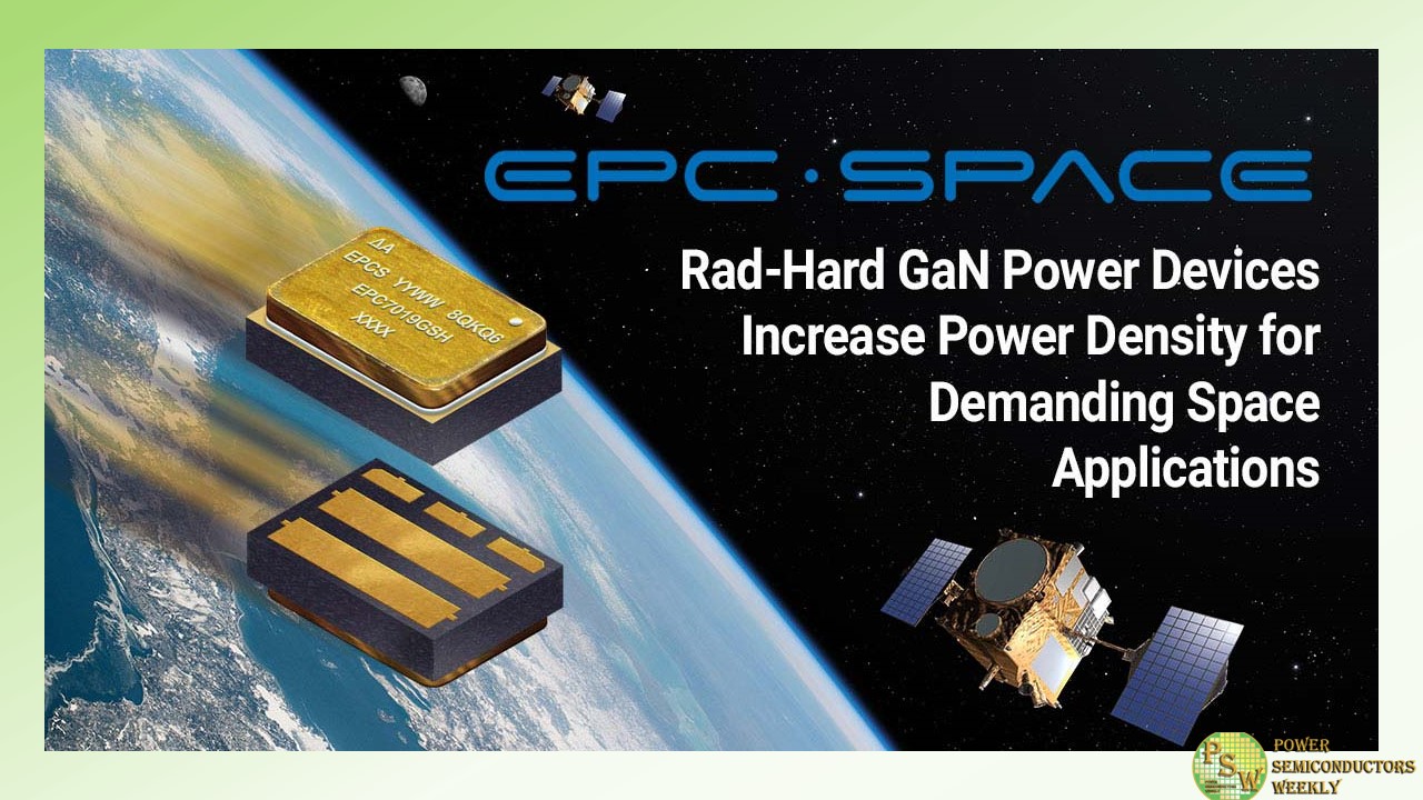
EPC Space announced the introduction of two new rad-hard GaN transistors with ultra-low on-resistance and high current capability for high power density solutions that are lower cost and more efficient than the nearest comparable radiation-hardened silicon MOSFET. These devices come packaged in hermetic packages in very small footprints.
The EPC7020G is a 200 V, 14.5 mΩ, 200 Apulsed radiation-hardened gallium nitride transistor and the EPC7030G is a 300 V, 32 mΩ, 200 Apulsed radiation-hardened gallium nitride transistor. These devices join the 40 V, 4.5 mΩ EPC7019G and the 100 V, 4.5 mΩ EPC7018G to cover applications including power supplies for satellites and space mission equipment, motor drives for robotics, instrumentation and reaction wheels, and deep space probes. This product family comes packaged in a compact hermetic package in a footprint less than 45 mm2.
Part Number Drain to Source Voltage (VDS) Drain to Source Resistance (RDS(on)) Single-Pulse Drain Current (IDM) EPC7019G 40 V 4 mΩ 530 A EPC7018G 100 V 6 mΩ 345 A EPC7020G 200 V 14.5 mΩ 200 A EPC7030G 300 V 32 mΩ 200 A With higher breakdown strength, lower gate charge, lower switching losses, better thermal conductivity, and lower on-resistance, power devices based on GaN significantly outperform silicon-based devices and enable higher switching frequencies resulting in higher power densities, higher efficiencies, and more compact and lighter weight circuitry for critical spaceborne missions.
“The G-Package family offers the lowest on-resistance of any packaged rad hard transistor currently on the market,” said Bel Lazar, CEO of EPC Space. “These devices offer mission-critical components with superior figure of merit, significantly smaller size, and lower cost for the space and other high-reliability markets than alternative rad hard silicon solutions”.
Original – EPC Space
-
Navitas Semiconductor will reveal a new, high-performance wide bandgap power platform as part of its display at one of Asia’s most prestigious electronics exhibitions – sponsored by Navitas – SEMICON Taiwan 2023, from September 6th-8th.
Visitors will discover the latest gallium nitride (GaN) GaNFast™ power ICs integrate gallium nitride (GaN) power and drive, with control, sensing, and protection to enable faster charging, higher power density, and greater energy savings. Complementary GeneSiC™ power devices are optimized high-power, high-voltage, and high-reliability silicon carbide (SiC) solutions.
Additionally, Navitas will showcase cutting-edge, power-system platforms to dramatically accelerate customer developments, minimize time-to-market, and set new industry benchmarks in energy efficiency, power density and system cost. These system platforms include complete design collateral with fully-tested hardware, embedded software, schematics, bill-of-materials, layout, simulation and hardware test results. Examples include:
- Navitas’ CRPS185 data center power platform, that delivers a full 3,200 W of power in only 1U (40 mm) x 73.5mm x 185 mm (544 cc), achieving 5.9 W/cc, or almost 100 W/in3 power density. This is a 40% size reduction vs, the equivalent legacy silicon approach and reaches over 96.5% efficiency at 30% load, and over 96% stretching from 20% to 60% load, creating a ‘Titanium Plus’ benchmark.
- Navitas’ 6.6 kW 3-in-1 bi-directional EV on-board charger (OBC) with 3 kW DC-DC. This 96%+ efficient unit has over 50% higher power density, and with efficiency over 95%, delivers up to 16% energy savings as compared to competing solutions.
As part of SEMICON’s Power and Opto Semiconductor Forum, Navitas’ Charles Bailley, Senior Director of Business Development, will present “GaN Power ICs Increase Power Density in EV Power Systems”. The presentation is at 2pm, on September 6th, in room 402, 4F, TaiNEX 1.
“Breakthrough high efficiency, high reliability, and high power density – all from the new GaN power IC platform,” said Kevin 汪時民 Wang, Manager of Navitas Taiwan. “The new platform announcement matches SEMICON’s theme of ‘Innovating the World through Semiconductors’ and our own mission to ‘Electrify Our World™’.”
Original – Navitas Semiconductor
-
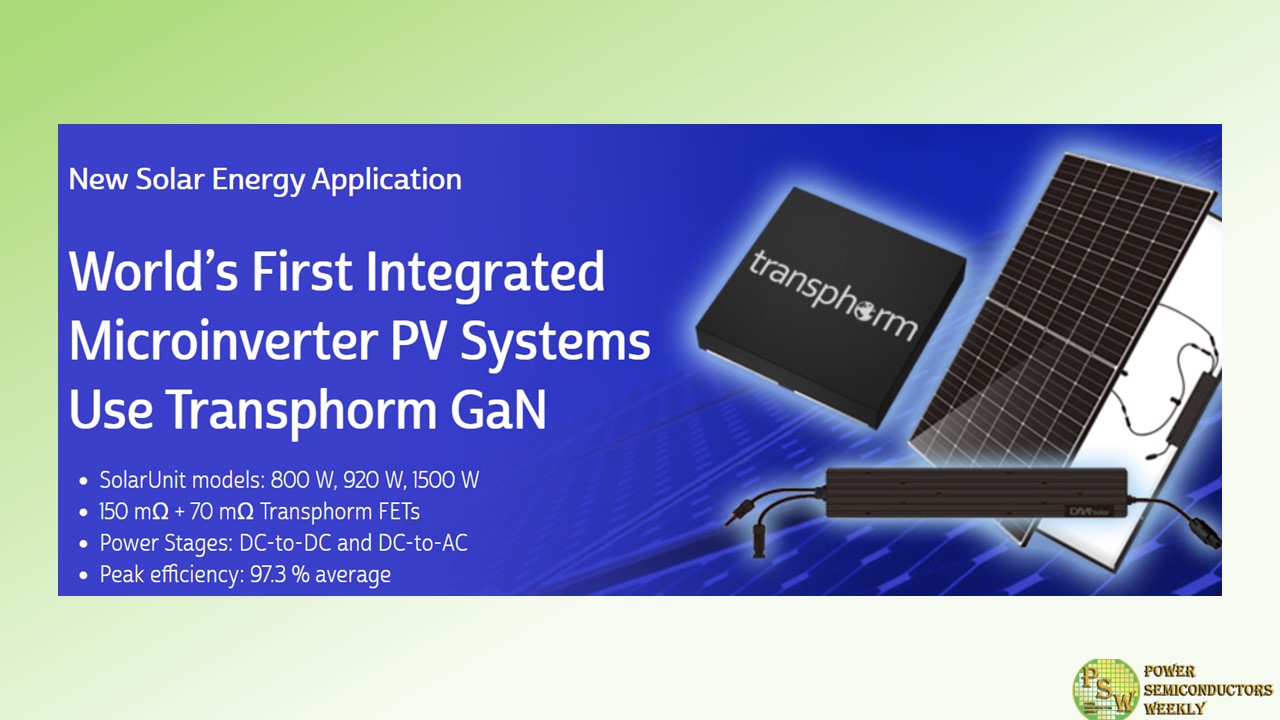
Transphorm, Inc. announced that its GaN platform powers the world’s first integrated photovoltaic (PV) systems from DAH Solar Co., Ltd. (Anhui Daheng New Energy Technology Co., LTD/subsidiary of DAH Solar). The PV systems are used in DAH Solar’s new SolarUnit product line. DAH Solar credits Transphorm’s GaN FETs with enabling it to produce smaller, lighter, and more reliable solar panel systems that also offer higher overall power generation with lower energy consumption.
The design achievements continue to demonstrate Transphorm’s One Core GaN Platform, Crossing the Power Spectrum leadership position by solidifying its value proposition in the renewables market, which currently represent a GaN TAM of more than $500M.
DAH Solar uses Transphorm’s 150 mΩ and 70 mΩ GaN FETs in the SolarUnits’ design architecture (both DC-to-DC and DC-to-AC power stages). The SolarUnits are available in three models with power outputs of 800 W, 920 W, or 1500 W and peak efficiencies of 97.16%, 97.2%, and 97.55% respectively. The GaN devices deliver higher switching frequencies and power density versus incumbent silicon solutions. Notably, the two FETs are available in PQFN88 performance packages that pair with commonly-used gate drivers—features that helped DAH Solar quicken its design time.
“We have a strong legacy of producing innovative PV products. As such, we consistently look for ways to advance our products with state-of-the-art technologies to create a better, more efficient end user experience,” said Yong Gu, GM, DAH Solar. “We view Transphorm as an authority in the field of GaN production and found their advanced GaN FETs to be the optimal devices for our new SolarUnit line. The devices are easy to design in and offer performance advantages that enable us to continue building on our legacy.”
Transphorm today supports the largest range of power conversion requirements (45 W to 10+ kW) across the widest range of power applications. The company’s FET portfolio includes 650 V and 900 V devices with 1200 V devices in development. These FETs are JEDEC and AEC-Q101 qualified, making them optimal solutions for power adapters and computer PSUs through to broad industrial UPSs and electric vehicle mobility systems.
The company’s technology innovations continue to set new benchmarks across the GaN power semiconductor industry. In parallel, they help customers bring to market new, disruptive applications in their own markets—such as DAH Solar’s PV systems.
These achievements are due to Transphorm’s normally-off SuperGaN® platform, which uses the cascode d-mode configuration to harness GaN’s intrinsic advantages. The superior physics of this high performance GaN platform design delivers competitively unmatched benefits such as easier drivability, easier designability, higher reliability, and greater manufacturability.
“The value Transphorm’s GaN platform brings to a variety of applications continues to be demonstrated by market leaders like DAH Solar,” Kenny Yim, Vice President of Asia Sales, Transphorm. “Solar inverters as well as other high-power applications require highly reliable, high performing power semiconductors that can withstand decades of operation in harsh environments.
Using Transphorm’s SuperGaN technology helps reduce power loss thereby minimizing thermal stress on other designed-in components. That’s a phenomenal achievement over alternative GaN and Silicon solutions underscoring the benefits our GaN brings to next generation power systems.”
Original – Transphorm
-

The University of Arkansas celebrated an important milestone with the groundbreaking on a building that Chancellor Charles Robinson suggested might someday rival the U of A’s most iconic structure, Old Main, in significance to the university and the state of Arkansas.
Robinson and other university leaders, including University of Arkansas System President Don Bobbitt and members of the U of A System Board of Trustees, as well as researchers and industry leaders, gathered at the Arkansas Research and Technology Park in South Fayetteville to celebrate construction of the national Multi-User Silicon Carbide Research and Fabrication Facility, or MUSiC.
The new semiconductor research and fabrication facility will produce microelectronic chips made with silicon carbide, a powerful semiconductor that outperforms basic silicon in several critical ways. The facility will enable the federal government – via national laboratories – businesses of all sizes, and other universities to prototype with silicon carbide, a capability that does not presently exist elsewhere in the U.S.
Work at the facility will bridge the gap between traditional university research and the needs of private industry and will accelerate technological advancement by providing a single location where chips can go from developmental research to prototyping, testing and fabrication.
“This fills a gap for our nation, allowing companies, national laboratories and universities around the nation to develop the low-volume prototypes that go from their labs to fab, ultimately scaling up to the high-volume manufacturing…” said Alan Mantooth, Distinguished Professor of electrical engineering and principal investigator for the MUSiC facility. “We fill that gap. And there’s no other place like it in the world. This is the only place that will be able to do that with silicon carbide.”
The 18,660 square-foot facility, located next to the National Center for Reliable Electrical Power Transmission at the research and technology park, will address obstacles to U.S. competitiveness in the development of silicon-carbide electronics used in a wide range of electronic devices, circuits and other consumer applications. The building will feature approximately 8,000 square feet of clean rooms for fabrication and testing.
Education and training within the facility will also accelerate workforce development, helping supply the next generation of engineers and technicians in semiconductor manufacturing, which Mantooth and other leaders have said is critical for bringing semiconductor manufacturing back to the U.S., after it was offshored in the late 1990s and early 2000s.
“This is truly a special day in the life of the University of Arkansas,” said Robinson. “This building, it really doesn’t need to be hyped. It is a very important building, and you just know it, important for our university, important for our state, important for our nation.”
Robinson invoked another groundbreaking, that of Old Main, the university’s oldest and best known structure, which the university celebrated Aug. 17, 1873, almost exactly 150 years ago.
“I took that 150th anniversary of the groundbreaking as a good sign that we are moving in a timely way,” Robinson said, “doing important work in establishing this building.”
Friday’s groundbreaking occurred a day after the university and the Arkansas Department of Commerce hosted the CHIPS AMERICA Summit, an event in which research, industry and governmental leaders discussed semiconductor-related opportunities resulting from the CHIPS (Creating Helpful Incentives to Produce Semiconductors) and Science Act passed by Congress in 2022. The event featured Adrienne Elrod, director of external and government affairs for the U.S. Department of Commerce’s CHIPS Program Office, U.S. Rep. Steve Womack and Arkansas Secretary of Commerce Hugh McDonald.
During the summit, Elrod stated that prior to the coronavirus pandemic, 90% of the world’s leading-edge chips were manufactured at one facility in Taiwan. The federal government prioritized the onshoring of this critical technology as a result of manufacturing and production shortages of essential computer chips during the pandemic.
“If America is going to compete and lead the world over the next century, we must invest in our technology and manufacturing,” Elrod said. “We want to make sure, at the very least, that we have two new large-scale clusters of leading- edge fabs created (in the United States).”
As Mantooth mentioned, the University of Arkansas can contribute to this effort on a fundamental level and is uniquely positioned to take advantage of opportunities offered by the CHIPS and Science Act, which is providing approximately $280 billion in funding to stimulate domestic research and manufacturing of semiconductors.
“The university is leaning forward and has now secured funding for projects important to microelectronics research and development,” Womack said during Thursday’s summit. “The university has positioned itself, as I say often, to be the preeminent university research location for microelectronics. … I am grateful for the bright minds at the University of Arkansas with a proven track record of success who will make this happen.”
Original – University of Arkansas
-

The rapid growth of technology over the past century brought us as many advantages as many disadvantages including the accelerating global warming with its dramatic consequences we face every day in various parts of the Earth. So far no one found a solution how to stop this process, but there are many solutions how to slow it down.
Today we try to respond to this challenge with carbon neutrality initiatives launched in many countries across the globe. And one of the major steps in this green society program is the electrification of passenger and commercial vehicles.
Right now, companies have various approaches to vehicle electrification including mild-hybrid electric vehicles MHEV, full hybrid electric vehicles HEV, plug-in hybrid electric vehicles PHEV, battery electric vehicles BEV, and fuel-cell electric vehicle FCEV. What some time ago seemed like a big step forward is a reality we live in now.
And to make this dream come true became possible with the help of power semiconductors. For a long time, semiconductors were used in the automotive industry, and the evolution of power semiconductor materials pushed the transition to the electrification of vehicles. Electric vehicles’ performance and cost depend on the technical level of the motor control system.
Previously, silicon (Si) IGBT modules served as the heart of electronic control systems with their relatively high switching speed and low conduction loss. But with the growth of silicon carbide (SiC) technology, EVs step into the new era of electrification.
Silicon-based semiconductors have been dominating the market for many decades. No wonder, several generations of power electronics engineers were passing their knowledge and experience working with silicon semiconductors. Through time they have short-listed their preferred solutions produced by several companies.
Based on the current requirements for the improvement of battery life and dynamic performance of electric passenger and commercial vehicles, higher efficiency, and fewer parts and materials are required to further improve the power density of inverters and electric drive assemblies. All this becomes possible with the transition from Si to SiC power devices. But when it comes to the all-new silicon carbide semiconductors and the rapidly growing EV industry, many face difficulties to make the right choice of the silicon carbide devices available in the market.
Recently I launched a poll to understand what is most important for EV companies when choosing a supplier of SiC power devices. Power electronics engineers from the semiconductor and automotive industries shared their experience and unanimously confirmed that the performance of the power devices plays a crucial role when choosing a supplier. The poll results are:
- Performance/characteristics – 66%
- Price – 16%
- Lead time – 9%
- Brand – 9%
Based on the results it is clear that for the EV market today characteristics of SiC power devices and price play the most important role. After all, consumers want high performance and reliability at affordable prices.
Nowadays SiC is still more expensive than Si. However, the prices have dropped a lot in the past decade, and the growing number of SiC fabs promises to drop the price in the future. Fingers crossed, in the nearest future, the dream of the consumers for the high-performance, reliable, and affordable EV will come true.
-
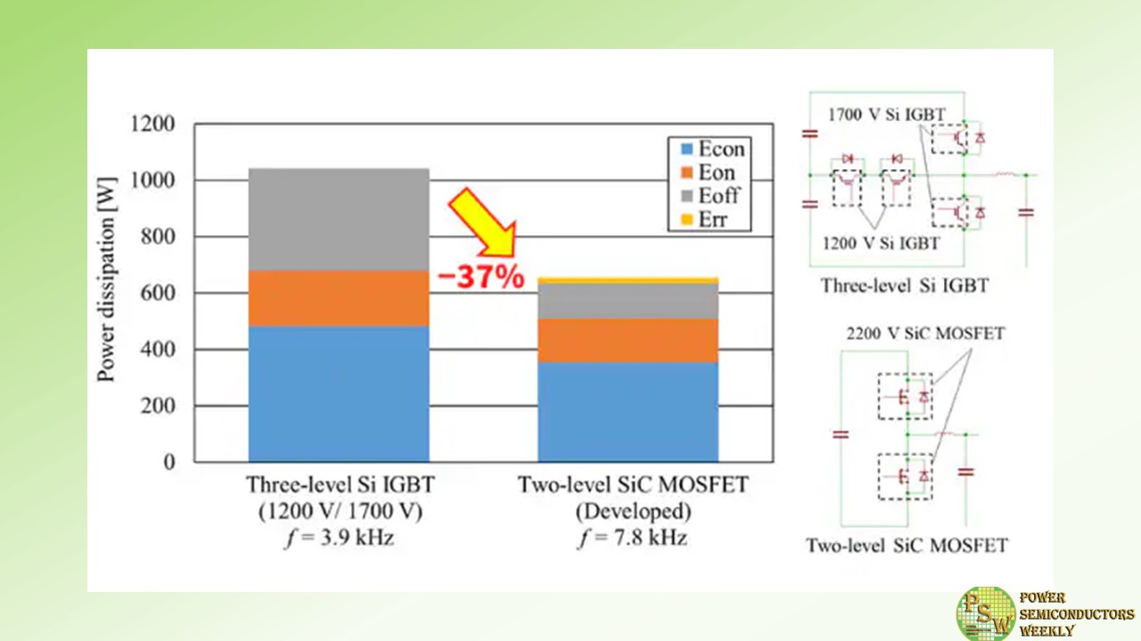
Toshiba Electronic Devices & Storage Corporation has developed 2200 V silicon carbide (SiC) metal oxide semiconductor field effect transistors (MOSFETs) for photovoltaic (PV) inverters. A two-level inverter with the new devices realized higher frequency operation and lower power loss than a conventional three-level silicon (Si) insulated gate bipolar transistor (IGBT) inverter. The new MOSFETs also contribute to simplification of inverter systems and reductions in their size and weight.
Three-level inverters enjoy the advantage of low switching losses because the voltage applied to switching devices in the inverters during off-state is half the line voltage. Against this, two-level inverters have fewer switching modules than three-level inverters, realizing a simpler, smaller, and lighter system. However, they require semiconductors with higher breakdown voltage, as the applied voltage is equal to the line voltage. Also, demand for semiconductors with both low loss and high breakdown voltage is growing as 1500 V DC line voltage systems are introduced in photovoltaic and other renewable energy markets.
Toshiba Electronic Devices & Storage Corporation has developed 2200 V Schottky barrier diode (SBD)-embedded SiC MOSFETs for two-level inverters in 1500 V DC voltage systems. The impurity concentration and thickness of the drift layer has been optimized to maintain the same relationship between the on-resistance and the breakdown voltage as our existing products, and also to achieve high resistance to cosmic rays, a requirement for PV systems. It has also been confirmed that embedding SBDs clamped parasitic PN junctions between the p-base regions and the n-drift layer secure high reliability in reverse conduction.
Switching energy loss for the developed all-SiC module is far lower than for the Si module (Si IGBTs + Si fast recovery diodes) with the same 2000 V rated voltage class. Estimates of inverter power dissipation found that the developed SiC module achieves higher frequency operation twice that of a conventional Si IGBT, as well as a 37% lower loss for the two-level SiC inverter against the three-level Si inverter. The higher frequency operation enables downsizing and weight reduction of other system components, such as heat sinks and filters.
Original – Toshiba
-

The University of Arkansas has taken the next step to becoming a national leader in the United States’ semiconductor economy. Semiconductors, such as silicon, are essential materials in most electronic devices and advance performance in fields such as healthcare, national defense, computing and transportation.
This August, the university began construction on the national Multi-User Silicon Carbide Research and Fabrication Facility, or MUSiC. Capable of silicon or silicon carbide chip fabrication, this new semiconductor research and fabrication facility will enable the government, businesses of all sizes, and universities to prototype in silicon carbide, introducing a capability that does not presently exist in the U.S.
This unique facility will offer low-volume prototyping for high-volume manufacturing, bridging the gap between traditional university research and the needs of private industry. This will accelerate both workforce development and technological advancement in semiconductors by providing a single location where chips can be go from developmental research to prototyping, testing and fabrication.
Alan Mantooth, Distinguished Professor of electrical engineering at the U of A, is principal investigator for MUSiC. He stated that with MUSiC, the university could “begin training the next generation at a variety of degree levels to provide well-trained and educated talent for onshoring semiconductor manufacturing that domestic suppliers offshored in the late 90s and early 2000s. Our training will be equally applicable to silicon and silicon carbide and other materials.”
Construction coincides with the CHIPS America Summit on Aug. 17, an invitation-only event for research, industry and governmental leaders from across the nation to discuss CHIPS and Science Act semiconductor-related opportunities and the ways in which the U of A and the State of Arkansas are uniquely positioned to lead.
The summit will feature Director of External and Government Affairs for the U.S Department of Commerce’s CHIPS Program Office, Adrienne Elrod. U.S. Representative Steve Womack and Arkansas Secretary of Commerce Hugh McDonald will also participate.
In addition to the MUSiC facility, the U of A is also home to the first Energy Frontier Research Center in Arkansas, as part of a team of researchers who received $10.35 million from the U.S. Department of Energy. The Center for Manipulation of Atomic Ordering for Manufacturing Semiconductors is dedicated to investigating the formation of atomic orders in semiconductor alloys and their effects on various physical properties. This research program will enable reliable, cost-effective and transformative manufacturing of semiconductors.
Researchers at the U of A previously established the MonArk NSF Quantum Foundry to accelerate the development of quantum materials and devices. In collaboration with Montana State University, and other member universities, the foundry supports the study of 2-D materials — consisting of a single layer of bonded atoms — by aiding researchers and facilitating the exchange of ideas across academia and industry. The project leads the fabrication of 2-D material quantum devices and their characterization, using low-temperature electronic transport and optoelectronic techniques.
The U of A’s existing and expanding research foundation means it’s uniquely positioned to take advantage of the recent CHIPS (Creating Helpful Incentives to Produce Semiconductors) and Science Act, which is providing approximately $280 billion in funding to stimulate domestic research and manufacturing of semiconductors.
As a result of manufacturing and production shortages of essential computer chips during the pandemic, which are overwhelmingly manufactured overseas, the federal government has prioritized the onshoring of this critical technology.
About the University of Arkansas: As Arkansas’ flagship institution, the U of A provides an internationally competitive education in more than 200 academic programs. Founded in 1871, the U of A contributes more than $2.2 billion to Arkansas’ economy through the teaching of new knowledge and skills, entrepreneurship and job development, discovery through research and creative activity while also providing training for professional disciplines.
The Carnegie Foundation classifies the U of A among the few U.S. colleges and universities with the highest level of research activity. U.S. News & World Report ranks the U of A among the top public universities in the nation. See how the U of A works to build a better world at Arkansas Research and Economic Development News.
The national Multi-User Silicon Carbide Research and Fabrication Facility, or MUSiC, will provide opportunities for the government and business of all sizes, and universities to prototype in silicon carbide, introducting a capability that does not currently exist in the U.S.
Original – University of Arkansas
-

Transphorm, Inc. announced it has demonstrated up to 5 microsecond short circuit withstand time (SCWT) on a GaN power transistor with a patented technology. The achievement is the first of its kind on record, marking an important milestone for the industry as a whole. It proves Transphorm GaN’s ability to meet the required short circuit capabilities of rugged power inverters such as servo motors, industrial motors, and automotive powertrains served traditionally by silicon IGBTs or silicon carbide (SiC) MOSFETs— an over $3 billion GaN TAM over the next 5 years.
The demonstration was developed with support from Yaskawa Electric Corporation, a long-term strategic partner of Transphorm’s and a global leader in low and medium voltage drives, servo systems, machine controllers, and industrial robots. This makes GaN a highly attractive power conversion technology for servo systems, as it allows for higher efficiency and reduced size compared to incumbent solutions.
To do that, GaN must pass stringent robustness tests—of which, short-circuit survivability is the most challenging. In case of short-circuit faults, the device must survive extreme conditions with both high current and high voltage. The system can take up to a few microseconds to detect the fault and shut down the operations. During this time, the device must withstand the fault on its own.
“If a power semiconductor device cannot survive short-circuit events, the system itself may fail. There was a strong perception that GaN power transistors could not meet the short circuit requirements needed for heavy-duty power applications such as ours,” said Motoshige Maeda, Department Manager of Fundamental R&D Management Department, Corporate Technology Division, Yaskawa. “Having worked with Transphorm for many years, we believed that perception to be unfounded and have been proven right today. We’re excited about what their team has accomplished and look forward to demonstrating how this new GaN feature can benefit our designs.”
The short-circuit technology has been demonstrated on a newly designed 15 mΩ 650 V GaN device. Notably, that device reaches a peak efficiency of 99.2% and a maximum power of 12 kW in hard-switching conditions at 50 kHz. The device demonstrated not only performance, but also reliability, passing high-temperature high-voltage stress requirements.
“Standard GaN devices can withstand short-circuit for only a few hundredths of nanoseconds, which is too short for fault detection and safe shut-down. However, with our cascode architecture and key patented technology, we were able to demonstrate short-circuit withstand time up to 5 microseconds with no additional external components, thus retaining low cost and high performance,” said Umesh Mishra, CTO and Co-Founder, Transphorm.
“We understand the demands of high-power, high-performance inverter systems. We have a long history of strong innovation, and we’re proud to say that experience helped us bring GaN to the next level. This is yet another validation of Transphorm’s global leadership in high voltage GaN robustness and reliability and will be a gamechanger for GaN in motor drives and other high-power systems.”
The full description explaining the SCWT achievement, the demonstration analysis, and more is expected to be presented at a major power electronics conference next year.
Original – Transphorm
