-

Infineon Technologies AG has been nominated for the Deutscher Zukunftspreis 2024, the Federal President’s Award for Technology and Innovation, for its development of a new type of energy-saving chip based on the innovative semiconductor material silicon carbide (SiC). The Jury of Deutscher Zukunftspreis has announced the three nominated teams in Munich.
A team of developers from Infineon, together with Chemnitz University of Technology, has succeeded in developing the world’s first silicon carbide MOSFET with a vertical channel (trench MOSFET) and innovative copper contacting in the 3300V voltage class. The new SiC modules and the power converters equipped with the modules represent a revolutionary innovation leap in semiconductor technology from conventional silicon to more energy-efficient silicon carbide, which reduces switching losses in high-current applications by 90%.
MOSFETs are electrical switches for a wide range of applications. Trench MOSFETs differ from so-called planar MOSFETs in their cell structure and performance. While the current flow in planar MOSFETs is initially horizontal, trench MOSFETs offer purely vertical channels. This results in a higher cell density per surface area, which in turn significantly reduces the losses in the chip during energy conversion and therefore increases efficiency.
“The transition towards green energy and many other pressing challenges of our time can only be solved with technological progress,” said Jochen Hanebeck, CEO of Infineon Technologies AG. “It is therefore important to promote and reward innovation and make it visible in society. The ‘Deutscher Zukunftspreis’ is the most important national award that is presented with this aim in mind. The nomination is a great honor for us and proof of the successful research and development work at Infineon. Congratulations to all colleagues involved!”
The CoolSiC™ XHP™2 module family enables significant energy savings, for example in industrial power generation in solar parks or wind turbines, in power transmission and, above all, in end consumption, where high energies in the megawatt range are required. A single train with a silicon carbide drive system can save around 300 MWh per year compared to the previous silicon-based solution. This is roughly equivalent to the annual consumption of 100 single-family homes. Together with drive technology manufacturers and rail operators, Infineon is making an important contribution to decarbonization. At the same time, local residents also benefit from the lower noise level of trains with SiC modules when they pass through residential areas.
Through numerous innovative developments in chip processing and design as well as contacting and module technology, the team led by Dr. Konrad Schraml, Dr. Caspar Leendertz (both Infineon) and Prof. Dr. Thomas Basler (Chemnitz University of Technology) has brought the 3300V CoolSiC XHP2 high-performance module to production readiness. With ten times greater reliability against thermomechanical stress and a significantly higher power density compared to silicon modules, the new silicon carbide module can also be used to electrify large drives in diesel locomotives, agricultural and construction machinery, aircraft and ships, which were previously reserved for fossil fuels. The significantly higher switching frequencies permitted by the new module are helpful, as they enable a significant reduction in weight and volume of the power converters in the application.
“This nomination shows that climate change and sustainable resource consumption have become central aspects of our society,” said Dr. Peter Wawer, Division President Green Industrial Power (GIP) at Infineon. “Innovative energy solutions and power semiconductors are a core component in decarbonization and fighting climate change, as the expert jury of Deutscher Zukunftspreis has recognized. I am proud that we at Infineon can make a significant contribution to a green future with pioneering technology.”
Project manager Dr. Konrad Schraml: “For us as a development team, it is a matter close to our hearts to develop innovative chips that contribute to efficient energy consumption and thus also to green mobility on our planet. This nomination is a great recognition for my team, whose tireless efforts, expertise and passion for sustainability have made the technology breakthrough in silicon carbide possible.”
On November 27, Federal President Frank-Walter Steinmeier presents the Deutscher Zukunftspreis to the winning team in Berlin.
Original – Infineon Technologies
-

Wolfspeed, Inc. unveiled a silicon carbide module designed to transform the renewable energy, energy storage, and high-capacity fast-charging sectors through improved efficiency, durability, reliability, and scalability. The 2300V baseplate-less silicon carbide power modules for 1500V DC Bus applications were developed and launched utilizing Wolfspeed’s state-of-the-art 200mm silicon carbide wafers.
Wolfspeed also announced that it is partnering with EPC Power, a premier North American utility-scale inverter manufacturer. EPC Power will be employing the Wolfspeed® modules in utility-grade solar and energy storage systems, which offer a scalable high-power conversion system and high-performance controls and system redundancy.
“The solar and energy storage market remains among the fastest-growing segments of the renewable energy industry. As the pioneers of silicon carbide, we are driven to create solutions that will open the door to a new era of modern energy,” said Jay Cameron, Wolfspeed Senior Vice President and General Manager, Power. “Energy efficiency, reliability, and scalability are top of mind for our customers, such as EPC Power, who recognize the substantial advantages Wolfspeed’s silicon carbide brings to the table.”
“Silicon carbide devices open the door to a step-change in inverter performance and reliability. With our commitment to extreme reliability, performance, and security in our new ‘M’ inverter while also forging a deep commercial relationship with key suppliers, Wolfspeed was the obvious choice,” said Devin Dilley, President and Chief Product Officer, EPC Power.
With mounting global investment in renewable energy, the solar energy market is estimated to reach a $300 billion market capitalization by 2032. According to the International Energy Agency (IEA), 2024-25 will see the highest energy demand growth rate since 2007, reinforcing the need for efficient and reliable clean power. Wolfspeed’s silicon carbide solution helps bridge this crucial gap, supporting the next era of modern energy technologies while reinforcing U.S. clean energy manufacturing leadership.
Cameron continued, “This platform further validates our investments in 200mm wafer technology and production as the potential of silicon carbide continues to be recognized by industry leaders across all mission-critical applications.”
Original – Wolfspeed
-
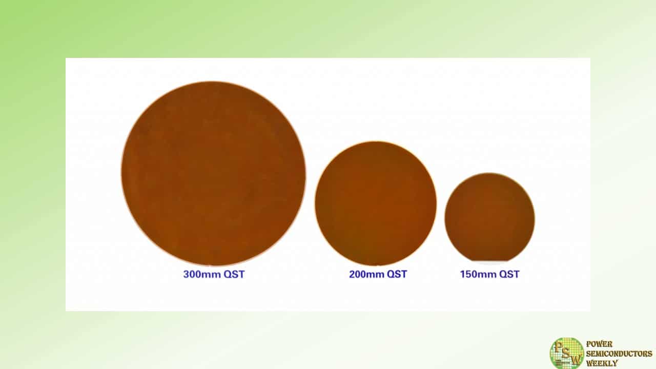
Shin-Etsu Chemical Co., Ltd. has created a 300-mm (12-inch) QSTTM substrate, which is a substrate dedicated to GaN epitaxial growth, and recently started supplying samples.
Shin-Etsu Chemical has sold 150-mm (6-inch) and 200-mm (8-inch) QSTTM substrates and GaN on QSTTM epitaxial substrates of each diameter. Meanwhile, the company worked on further increasing the diameter in response to strong customer demand and successfully developed a 300-mm (12-inch) QSTTM substrate. GaN device manufacturers cannot benefit from increasing the diameter of materials because of the lack in large-diameter substrate suitable for GaN growth, despite the fact that they can use the existing Si production line for GaN.
This 300-mm QSTTM substrate enables GaN epitaxial growth without warping or cracks, which was unattainable on Si substrates, thus significantly reducing device costs. In addition to the enhancement of facilities for 150-mm and 200-mm QSTTM substrates already in progress, Shin-Etsu Chemical will work on mass-producing 300-mm QSTTM substrates.
Since QSTTM substrates have the same coefficient of thermal expansion as that of GaN, it is possible to constrain warping and cracks of GaN epitaxial layer on QSTTM substrate of the SEMI standard thickness. This substrate material allows for high-quality and thick GaN epitaxial growth with a large diameter. Leveraging this feature, many customers are evaluating QSTTM substrates and GaN on QSTTM epitaxial substrates for power devices, high-frequency devices, and LEDs. Despite the challenging business environment, customers have entered the development phase toward practical to address the recently increasing interest in power devices, including power supplies for data centers.
The addition of the 300-mm QSTTM substrate to the lineup of the 150-mm and 200-mm can significantly accelerate the spread of GaN devices. Shin-Etsu Chemical is committed to contribute to the realization of a sustainable society where energy can be used efficiently through the social implementation of GaN devices.
Original – Shin-Etsu Chemical
-

North Carolina State University Professor B. Jayant Baliga has been awarded the 2024 Millennium Technology Prize for his work on the invention, development and commercialization of insulated gate bipolar transistors (IGBTs), which play a critical role in energy efficiency for technologies worldwide. The Millennium Technology Prize, which comes with a €1 million award, is the most prestigious international award focused on recognizing technological innovation.
The IGBT is an energy-saving semiconductor switch that controls the flow of power from an electrical energy source to any application that needs energy. The IGBT improves energy efficiency by more than 40 percent in an array of products, from cars and refrigerators to light bulbs, and is a critical component enabling modern compact cardiac defibrillators.
The IGBT has reduced global carbon dioxide emissions by over 82 gigatons (180 trillion pounds) over the past 30 years. This is equivalent to offsetting carbon dioxide emissions from all human activity for three years, based on average emissions of the past 30 years.
“The IGBT has already had and continues to have a major impact on supporting sustainability with improved living standards worldwide, while mitigating environmental impact,” says Minna Palmroth, chair of the Board of Technology Academy Finland, the foundation which awards the Millennium Technology Prize. “The main solution to tackle global warming is electrification and moving to renewable energy. The IGBT is the key enabling technology in addressing these issues.”
“It is very exciting to have been selected for this great honor,” says Baliga, who is the Progress Energy Distinguished University Emeritus Professor of Electrical and Computer Engineering at NC State.
“I am particularly happy that the Millennium Technology Prize will bring attention to my innovation, as the IGBT is an embedded technology that is hidden from the eyes of society. It has enabled a vast array of products that have improved the comfort, convenience and health of billions of people around the world while reducing carbon dioxide emissions to mitigate global warming. Informing the public of this impactful innovation will illustrate the betterment of humanity by modern technology.”
Baliga’s portfolio of 123 U.S. patents includes many other inventions that have also been commercialized. The split-gate power MOSFET is widely manufactured for use in laptops, PCs and servers. And his silicon carbide inventions – including the JBS rectifier and shielded channel power MOSFET – are used in a variety of state-of-the-art electrical power management technologies.
Baliga – who Forbes has called “the man with the world’s largest negative carbon footprint” – continues to work on technological challenges related to energy efficiency. He and his collaborators are currently working on new inventions to improve efficiencies related to solar power generation, electric vehicles and power delivery for AI servers.
The Millennium Technology Prize will be presented to Professor Bantval Jayant Baliga in Finland on Oct. 30 in an award ceremony that also celebrates the 20th anniversary of the prize. The prize will be presented by its patron, the president of Finland.
The €1 million Millennium Technology Prize is the preeminent award focused on technological innovations for a better life. This includes work that improves human well-being, biodiversity and wider sustainability. Overseen by the Technology Academy Finland, it was first awarded in 2004, and its patron is the President of Finland. Winners are selected by a distinguished international panel of experts from academia and industry. Innovations must be backed up by rigorous academic and scientific research and fulfill several criteria, including promoting sustainable development and biodiversity, having generated applications with commercial viability, and creating accessible socio-economic value.
Past winning innovations range from DNA sequencing that helped to develop COVID-19 vaccines, to ethical stem-cell research and versatile, affordable smart technology. Visit the Millennium Prize website for more information.
Original – North Carolina State University
-

ROHM announced the adoption of power modules equipped with 4th generation SiC MOSFET bare chips for the traction inverters in three models of ZEEKR EV brand from Zhejiang Geely Holding Group (Geely), a top 10 global automaker. Since 2023, these power modules have been mass produced and shipped from HAIMOSIC (SHANGHAI) Co., Ltd. – a joint venture between ROHM and Zhenghai Group Co., Ltd. to Viridi E-Mobility Technology (Ningbo) Co., Ltd, a Tier 1 manufacturer under Geely.
Geely and ROHM have been collaborating since 2018, beginning with technical exchanges, then later forming a strategic partnership focused on SiC power devices in 2021. This led to the integration of ROHM’s SiC MOSFETs into the traction inverters of three models: the ZEEKR X, 009, and 001. In each of these EVs, ROHM’s power solutions centered on SiC MOSFETs play a key role in extending the cruising range and enhancing overall performance.
ROHM is committed to advancing SiC technology, with plans to launch 5th generation SiC MOSFETs in 2025 while accelerating market introduction of 6th and 7th generation devices. What’s more, by offering SiC in various forms, including bare chips, discrete components, and modules, ROHM is able to promote the widespread adoption of SiC technology, contributing to the creation of a sustainable society.
Original – ROHM
-

Texas Instruments (TI) and the U.S. Department of Commerce have signed a non-binding Preliminary Memorandum of Terms for up to $1.6 billion in proposed direct funding under the CHIPS and Science Act to support three 300mm wafer fabs already under construction in Texas and Utah. In addition, TI expects to receive an estimated $6 billion to $8 billion from the U.S. Department of Treasury’s Investment Tax Credit for qualified U.S. manufacturing investments. The proposed direct funding, coupled with the investment tax credit, would help TI provide a geopolitically dependable supply of essential analog and embedded processing semiconductors.
“The historic CHIPS Act is enabling more semiconductor manufacturing capacity in the U.S., making the semiconductor ecosystem stronger and more resilient,” said Haviv Ilan, president and CEO of Texas Instruments. “Our investments further strengthen our competitive advantage in manufacturing and technology as we expand our 300mm manufacturing operations in the U.S. With plans to grow our internal manufacturing to more than 95% by 2030, we’re building geopolitically dependable, 300mm capacity at scale to provide the analog and embedded processing chips our customers will need for years to come.”
Since its founding more than 90 years ago, TI has been advancing technology, pioneering the transition from vacuum tubes to transistors and then to integrated circuits. Today, TI is the largest U.S. analog and embedded processing semiconductor manufacturer. TI chips are essential in nearly every type of electronic device, from cars with advanced safety and intelligence systems to life-saving medical equipment and smart appliances that make homes safer and more efficient.
The proposed direct funding under the CHIPS Act would support TI’s investment of more than $18 billion through 2029, which is part of the company’s broader investment in manufacturing. This proposed direct funding will support three new wafer fabs, two in Sherman, Texas, (SM1 and SM2) and one in Lehi, Utah (LFAB2), specifically to:
- Construct and build the SM1 cleanroom and complete pilot line for first production;
- Construct and build the LFAB2 cleanroom for first production; and
- Construct the SM2 shell.
These connected, multi-fab sites benefit from shared infrastructure, talent and technology sharing, and a strong network of suppliers and community partners. They will produce semiconductors in 28nm to 130nm technology nodes, which provide the optimal cost, performance, power, precision and voltage levels required for TI’s broad portfolio of analog and embedded processing products.
“With this proposed investment from the Biden-Harris Administration in TI, a global leader of production for current-generation and mature-node chips, we would help secure the supply chain for these foundational semiconductors that are used in every sector of the U.S. economy, and create tens of thousands of jobs in Texas and Utah,” said U.S. Secretary of Commerce Gina Raimondo. “The CHIPS for America program will supercharge American technology and innovation and make our country more secure – and TI is expected to be an important part of the success of the Biden-Harris Administration’s work to revitalize semiconductor manufacturing and development in the U.S.”
With a long history of supporting its employees to build long-term, successful careers, TI is also investing in building its future workforce. TI will create more than 2,000 company jobs across its three new fabs in Texas and Utah, along with thousands of indirect jobs for construction, suppliers and supporting industries.
“We are proud to work with Texas Instruments as they build new semiconductor fabs in Sherman and solidify Texas as the best state for semiconductors. Texas Instruments invented the microchip in Texas, and we are honored to be home to TI’s semiconductor manufacturing facilities in Dallas, Richardson and Sherman,” said Texas Gov. Greg Abbott. “With this latest project, TI is building on its more than 90-year legacy in Texas and adding thousands of good-paying jobs for Texans to manufacture critically important technology.”
“By investing in semiconductor manufacturing, we are helping secure this vulnerable supply chain, boosting our national security and global competitiveness, and creating new jobs for Texans,” said U.S. Sen. John Cornyn. “The chipmaking capabilities these resources will enable at Texas Instruments will help the U.S. reclaim its leadership role in the critically important semiconductor industry, and I look forward to seeing more Texas-led advancements in the years to come.”
In order to build a future-ready workforce, TI is enhancing the skills of current employees, expanding internships and creating pipeline programs with a focus on building electronic and mechanical skills. TI has robust engagements with 40 community colleges, high schools and military institutions across the U.S. to develop future semiconductor talent.
“Utah is thrilled that Texas Instruments is expanding its manufacturing presence in the Silicon Slopes, furthering the impact Utahns have on critical semiconductor technology,” said Utah Gov. Spencer Cox. “This investment in semiconductor manufacturing not only creates more jobs, but also brings supply chains back to the United States.”
“This proposed CHIPS funding will further support Texas Instruments’ investment in its new semiconductor fab in Lehi —and enhance Utah’s vital role in our national defense and economic success,” said U.S. Senator Mitt Romney. “I was an original sponsor of the CHIPS and Science Act—which made today’s announcement possible—because in order to compete on the world stage, we must continue to promote innovation, foster scientific talent, and expand research here at home. Texas Instruments’ expanded operations will help make the United States more self-reliant for chips essential to our national security and economy.”
TI has a long-standing commitment to responsible, sustainable manufacturing and environmental stewardship. As part of this commitment, TI continually invests in its fabrication processes and equipment to reduce energy, material and water consumption, and greenhouse gas (GHG) emissions.
The company’s 300mm wafer fabs will be entirely powered by renewable electricity. Additionally, all of TI’s new 300mm fabs are designed to meet LEED Gold standards for structural efficiency and sustainability. TI’s 300mm manufacturing facilities bring advantages in reducing waste and improving water and energy consumption per chip.
TI semiconductors are and will increasingly play a critical role in helping reduce the impact on the environment, helping customers create smaller, more efficient and cost-effective technology solutions that in turn drive continued innovation in electrification and the expanded usage of renewable energy.
Original – Texas Instruments
-
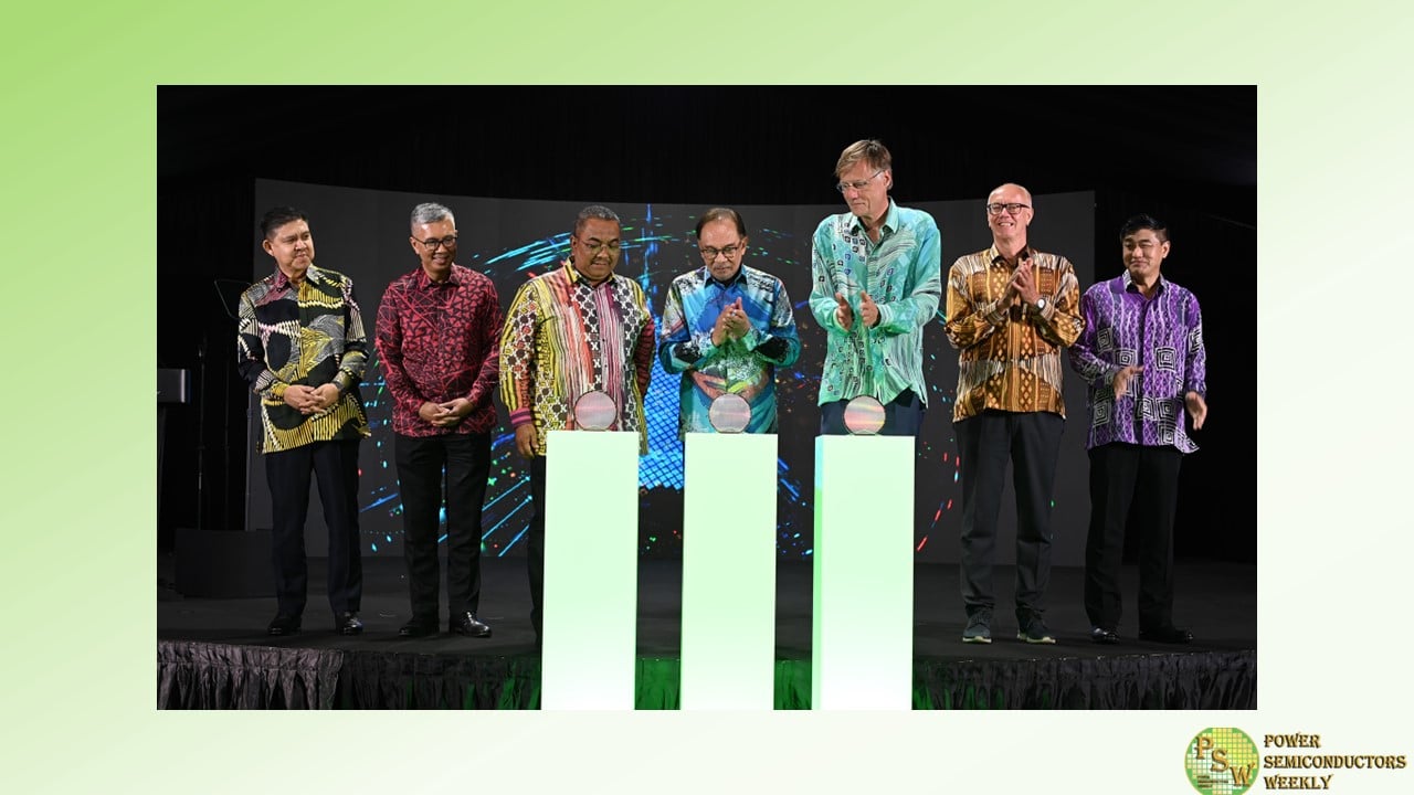
As global decarbonization efforts drive demand for power semiconductors, Infineon Technologies AG has officially opened the first phase of a new fab in Malaysia that will become the world’s largest and most competitive 200-millimeter silicon carbide (SiC) power semiconductor fab. Malaysian Prime Minister YAB Dato’ Seri Anwar Ibrahim and Chief Minister of the state of Kedah YAB Dato’ Seri Haji Muhammad Sanusi Haji Mohd Nor joined Infineon CEO Jochen Hanebeck, to symbolically launch production.
The highly efficient 200-millimeter SiC power fab will strengthen Infineon’s role as the global leader in power semiconductors. The first phase of the fab, with an investment volume of two billion euros, will focus on the production of silicon carbide power semiconductors and will include gallium nitride (GaN) epitaxy. SiC semiconductors have revolutionized high-power applications because they switch electricity even more efficiently and enable even smaller designs.
SiC semiconductors increase efficiency in electric vehicles, fast charging stations and trains as well as renewable energy systems and AI data centers. 900 high-value jobs will be created already in the first phase. The second phase, with an investment of up to five billion euros, will create the world’s largest and most efficient 200-millimeter SiC power fab. Overall, up to 4.000 jobs will be created with the project.
“New generations of power semiconductors based on innovative technology such as silicon carbide are an absolute prerequisite to achieving decarbonization and climate protection. Our technology increases the energy efficiency of ubiquitous applications such as electric cars, solar and wind power systems and AI data centers. We are therefore investing in the largest and most efficient high-tech SiC production facility in Malaysia, backed by strong customer commitments,” said Jochen Hanebeck, CEO of Infineon Technologies AG. “Since the demand for semiconductors will constantly rise, the investment in Kulim is highly attractive to our customers, who are backing it with their prepayments. It also increases the resilience of the supply chain for critical components needed for the green transition.”
“Infineon’s remarkable project reinforces Malaysia’s position as a rising major global semiconductor hub” says Malaysian Prime Minister YAB Dato’ Seri Anwar Ibrahim. “This major investment, which will locate the world’s largest and most competitive SiC power fab on our shores, will create jobs and opportunities, as well as attract suppliers, universities and top talent. Moreover, it will support Malaysia’s efforts to protect our climate by boosting electrification and increasing the efficiency of many applications, including electric cars and renewable energy. Thus, technology made in Malaysia will become a central part of global decarbonization efforts in the future.”
“Infineon’s deeply rooted presence in Kulim is a testament to the region’s potential as a hub for high-tech industries,” says Kedah Chief Minister YAB Muhammad Sanusi Md Nor. “This investment will not only create high-value job opportunities for the local community, it will also catalyze economic growth in the region. We are committed to continue providing top business conditions in Kedah and supporting Infineon’s efforts to establish a leading semiconductor facility in Kulim, which will have a positive ripple effect on the entire ecosystem.”
Infineon has secured design wins with a total value of approximately five billion euros and has received approximately one billion euros in prepayments from existing and new customers for the ongoing expansion of the Kulim 3 fab. Notably, these design wins include six OEMs in the automotive sector as well as customers in the renewable energy and industrial segments.
Kulim 3 will be closely connected to the Infineon site in Villach, Austria, Infineon’s global competence center for power semiconductors. Infineon already increased capacity for SiC and GaN power semiconductors in Villach in 2023. As “One Virtual Fab” for wide-bandgap technologies, both manufacturing sites now share technologies and processes which allow for fast ramping and smooth and highly efficient operation. The project also offers a high grade of resilience and flexibility, which will ultimately benefit Infineon’s customers.
The expansion will benefit from the excellent economies of scale already achieved for 200-millimeter manufacturing in Kulim. It will complement Infineon’s leading position in silicon, based on 300-millimeter manufacturing in Villach and Dresden. Thus, Infineon is strengthening its technological leadership across the entire spectrum of power semiconductors, in silicon as well as SiC and GaN.
In addition, the investment in wide-bandgap capacity in Kulim strengthens the local ecosystem and proves that Infineon is a reliable partner within the growing semiconductor hub Malaysia. Infineon’s operations in Malaysia started as early as 1973 in Melaka. In 2006, the company opened Asia’s first frontend fab in Kulim. Currently, Infineon employs more than 16.000 highly skilled people in Malaysia.
The Kulim 3 fab will be powered by 100% green electricity and will employ the latest energy efficiency measures to support Infineon’s goal of carbon neutrality. To avoid emissions, Infineon will use a state-of-the-art abatement system and green refrigerants that combine high efficiency with extremely low global warming potential. Other measures to ensure sustainable operations include state-of-the-art recycling of indirect materials and state-of-the-art water efficiency and recycling processes. Infineon is working towards recognition with the renowned Green Building Index certification.
Original – Infineon Technologies
-

Dominic Dorfner, Senior Vice President of the Automotive Division in Semikron Danfoss, will take over as President, when Claus A. Petersen retires on August 31, after 40 years in the Danfoss Group – the last 26 years leading Danfoss Silicon Power and Semikron Danfoss.
Dominic Dorfner has been named new President of Semikron Danfoss – a leading global manufacturer of power electronics based in Germany and part of the Danfoss Group. Dominic Dorfner joined Semikron Danfoss in 2021 as Head of the Industry Business in Danfoss Silicon Power. For the past 13 months he has been leading the Automotive Division in Semikron Danfoss.
Chairman of the Semikron Danfoss Board, Danfoss Power Electronics and Drives Segment president Mika Kulju says:
“The Board of Directors for Semikron Danfoss are very pleased that Dominic Dorfner has accepted the role as President. It is an important continuation of the work that has been done in Semikron Danfoss since the company was established two years ago with the merger of Danfoss Silicon Power and SEMIKRON. We are very excited to be working with him to continue the growth and realizing the huge potential for Semikron Danfoss in energy efficiency, in electrification, and in green energy.
Dominic Dorfner is taking over for Claus A. Petersen – a renowned name in the power electronics industry.
Claus A. Petersen has been with Danfoss for more than 40 years. He was named President of Semikron Danfoss when the merger was finalized in 2022. Before the merger he was leading Danfoss Silicon Power, a position he has held since the company was established in Schleswig-Holstein in 1998 with, at that time only around 20 employees. Today, Semikron Danfoss has around 4,000 global employees and annual sales over EUR 1 billion.
Though now retiring as company President, Claus A. Petersen is not completely leaving Semikron Danfoss, as he has joined the Board of Directors.
“We are fully committed to the ambitions and the strategy for Semikron Danfoss that has been developed under Claus’ leadership. I want to extend a big thank you to him, both for what he has accomplished, and for accepting to join the Board. This will ensure a very smooth and proficient transition,” says Mika Kulju, and continues: “Dominic Dorfner has big shoes to fill, but he has all the needed qualities to do so, and strong teams around him.”
Efficient power electronics are vital for decarbonization. Yet another reason why the new President of Semikron Danfoss is really excited about the challenge ahead.
Says Dominic Dorfner:
“Our purpose is to enable a huge transformation towards a CO2 neutral world for us and our kids. To do so, we need extensive electrification, we need green energy, and we need to save energy much more through energy efficiency. All that needs power electronics with the best power modules and systems out there. We can provide that, and I can’t think of a better reason to wake up early and go to work.”
First day in the new role for Dominic Dorfner will be September 1, 2024.
Original – Semikron Danfoss
-
Many different trends are taking center stage in both consumer electronics and industrial applications, such as portability, electrification, and weight reduction. All of these trends require compact and efficient designs. They also go hand in hand with unconventional PCB designs with severe space constraints that limit the use of external components.
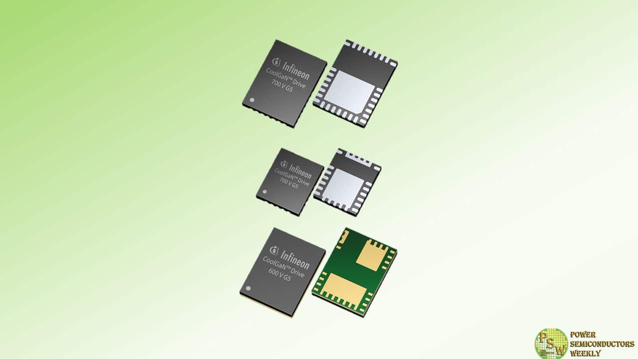
To address these challenges, Infineon Technologies AG expands its GaN portfolio with the CoolGaN™ Drive product family. It consists of the CoolGaN Drive 700 V G5 single switches, integrating one transistor plus gate driver in PQFN 5×6 and PQFN 6×8 packages, as well as the CoolGaN Drive HB 600 V G5 devices, combining two transistors with integrated high- and low-side gate drivers in a LGA 6×8 package. The new product family enables improved efficiency, reduced system size, and overall cost savings. This makes the devices suitable for longer-range e-bikes, portable power tools, and lighter-weight household appliances such as vacuums, fans, and hairdryers.
“For several years, Infineon has been focused on accelerating innovation in GaN to provide targeted solutions for real-world power challenges”, said Johannes Schoiswohl, Senior Vice President & General Manager, GaN Systems Business Line Head at Infineon. “The new CoolGaN Drive product family is another proof point of how we support our customers in developing compact designs with high power density and efficiency through GaN.”
The CoolGaN Drive family offers a wide range of single switches and half bridges with integrated drivers based on the recently announced CoolGaN Transistors 650 V G5. Depending on the product group, the components feature a bootstrap diode and are characterized by loss-free current measurement, and adjustable switch-on and switch-off dV/dt. They also provide OCP/OTP/SCP protection functions. As a result, the devices enable higher switching frequencies, leading to smaller and more efficient system solutions with high power density. At the same time, the bill of materials (BoM) is reduced. This not only results in a lower system weight, but also reduces the carbon footprint.
Samples of the half-bridge solutions are available now. Single-switch samples will be available starting Q4 2024. Further information is available at www.infineon.com/GaN-innovations.
Original – Infineon Technologies
-
According to a survey by Global Market Insights, Super Junction MOSFETs captured over 30% market share in the energy and power sector in 2023. Their applications span multiple domains, including electric vehicle charging stations, server and data center power supplies, LED drivers, solar inverters and home appliance controls.
The global Super Junction MOSFET market is projected to achieve a compound annual growth rate (CAGR) exceeding 11.5% by 2032. Super Junction MOSFETs offers robust assurance to customers seeking exceptional performance and stability backed by WeEn’s well-established reliability standards, comprehensive supply chain systems and continuously evolving technological roadmaps.
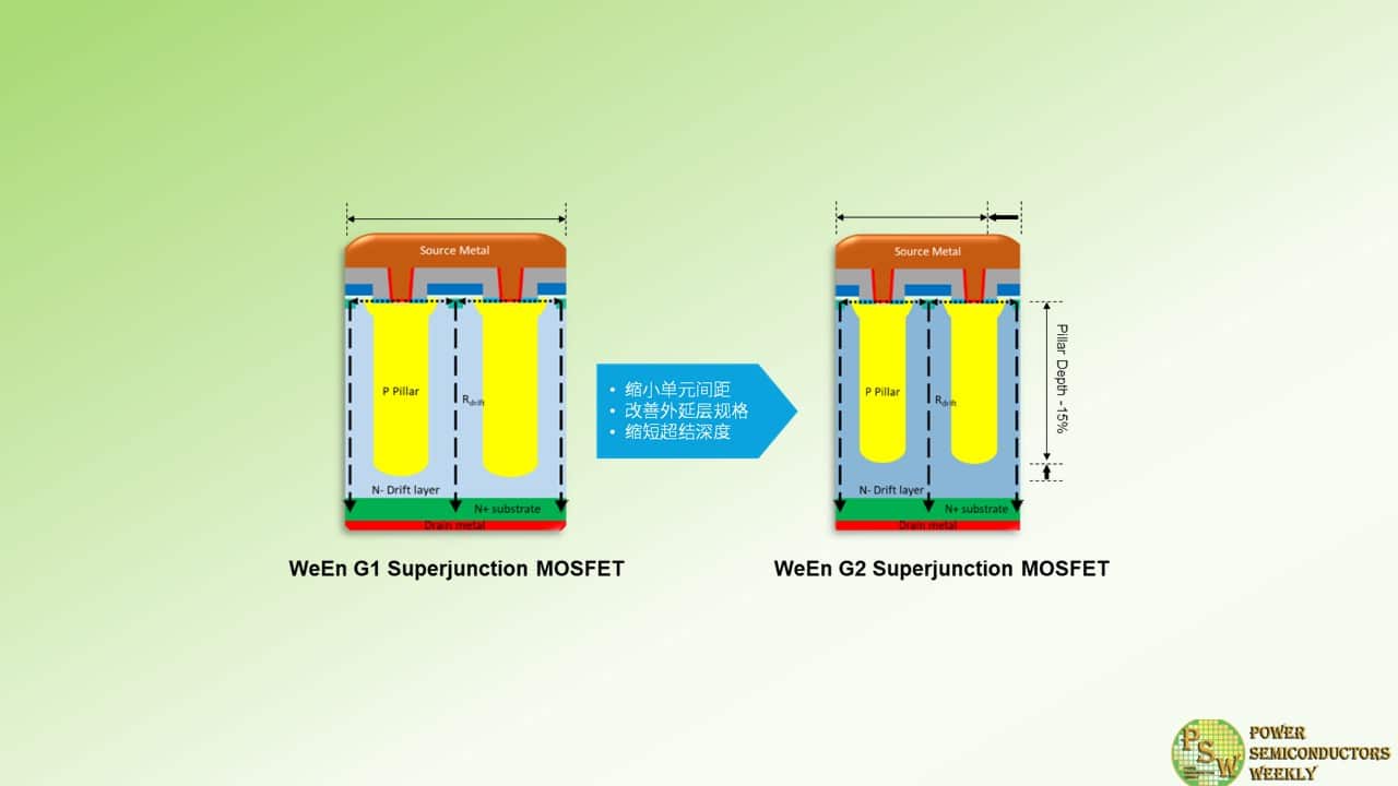
WeEn currently offers two series of Super Junction MOSFETs: G1 and G2. G2 Super Junction MOSFETs feature advanced design improvements, such as reduced cell pitch, low-resistance epitaxial layers, and shorter P-column depths. These innovations significantly reduce the device’s on-state resistance.
Simultaneously, WeEn precisely controlled the charge balance of the super junction structure, ensuring excellent avalanche ruggedness and low capacitive losses. This results in a balanced, outstanding performance in both hard and soft-switching applications that demand high efficiency, reliability, and superior thermal management.
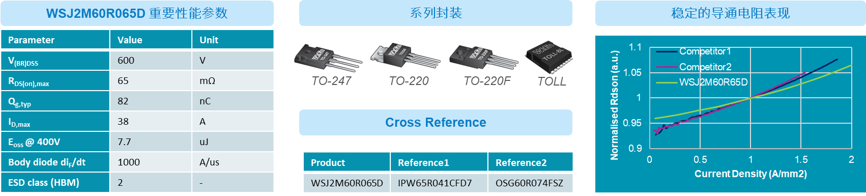
The WSJ2M60R065D is one of the flagship products in WeEn’s G2 Super Junction MOSFET lineup. Available in various packages including TO-220, TO-220F, TO-247, and TOLL. It particularly excels in terms of on-state resistance. Compared to competitors’ products, the WSJ2M60R065D maintains more stable on-state resistance across different current densities. Within its maximum continuous current range, the resistance variation does not exceed 10%. This stability provides customers with reliable performance data. Furthermore, the WSJ2M60R065D adapts well to applications with varying power requirements, demonstrating exceptional performance across diverse and complex operating environments.
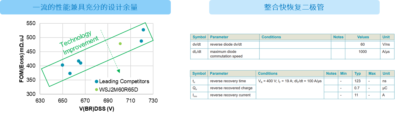
WeEn’s G2 MOSFETs are at the forefront of performance, with their Figure of Merit (FOM) on par with top global competitors. While ensuring stringent yield and process control, WeEn reserves more breakdown voltage margin for customers. 600V devices approach the standards of 650V devices available on the market, thoroughly safeguarding the reliability of customer applications. Moreover, the G2 MOSFET integrates a finely tuned fast recovery body diode, with a reverse recovery time (Trr) of only 123 ns. The body diode can withstand a commutation speed of 1000 A/μs without damage. This makes the WSJ2M60R065D particularly suitable for Zero Voltage Switching (ZVS) applications in soft-switching topologies, delivering high efficiency while handling irregular operating conditions.
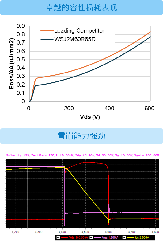
However, the WSJ2M60R065D is not limited to soft-switching applications. It also demonstrates excellent performance in hard-switching applications. The WSJ2M60R065D offers significant advantages in terms of lower capacitive losses (Eoss) compared to top competitors. Additionally, its normalized ruggedness is significantly higher than the industry standard, enabling it to withstand higher overvoltage and oscillation. It also demonstrates stable and safe performance in hard-switching topologies such as Power Factor Correction (PFC) circuits.
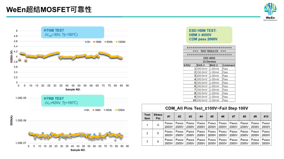
WeEn consistently adheres to rigorous and reliable quality assessment practices. In accelerated aging tests, the company maintains a zero-tolerance policy for product failures. WeEn MOSFET products demonstrate excellent consistency in performance during high-temperature stress aging tests at 168, 500, and 1000 hours. Furthermore, WeEn conducts additional reviews of the ESD (Electrostatic Discharge) capability of the device to minimize quality issues during production, packaging, and transportation. The WSJ2M60R065D demonstrates a robust quality level with a CDM (Charged Device Model) capability exceeding 2000V and an HBM (Human Body Model) capability of over 4000V.
Original – WeEn Semiconductors
