-
“The 31st International Optoelectronics Exposition (OPTO Taiwan)”, organized by Photonics Industry & Technology Development Association, is taking place in Taipei Nangang Exhibition Hall 1 from October 25th to 27th, for a three-day technological extravaganza. As a leading company in semiconductor technology, GlobalWafers unveils its latest achievements in compound semiconductors.
At this year’s exposition, GlobalWafers features 8”N type SiC crystal growth technology, Thinning technology of 6”and 8”SiC wafers, and high-value niche products in the GaN epitaxy field, demonstrating its technical prowess honed over many years in the compound semiconductor industry. SiC crystal growth presents challenges due to the need for growth in extremely high-temperature sealed environments, with factors like hot zone design and crucible materials in crystal growth furnace adding the complexity to equipment and operations.
GlobalWafers independently designs and develops 8”SiC-specific Physical Vapor Transport Method Grower (PVT) to further reduce crystal growth costs while achieving higher material quality control. Through outstanding technical control and production efficiency, as well as continuous research and development, GlobalWafers overcomes the technical challenges of SiC crystal growth, successfully moving forward to 8 inches, providing customers with high-quality, superior-performance SiC materials.
The high hardness and brittleness of SiC make subsequent wafering process extremely challenging. Leveraging its edge in wafer processing, GlobalWafers has successfully developed SiC ultra-thin thinning technology, showcasing 6” 90µm and 8”350µm ultra-thin polished SiC wafers at the exhibition. Ultra-thin SiC wafers offer advantages in lightweighting, heat dissipation, thermal conductivity, high-frequency operation, component miniaturization, and material costs, making them an ideal choice for high-performance semiconductor devices.
GlobalWafers’ SiC wafers include 4”~ 6” semi-insulating wafers and 6”~ 8”conductive SiC wafers, offering a comprehensive range of products to cater for diverse customer needs and expand into various fields of application.
Heteroepitaxy of GaN poses various technical challenges, such as lattice mismatch, stress, and defects. GlobalWafers focuses on research and development, launching a full range of GaN heteroepitaxy products, including silicon, SiC and sapphire substrates. A variety of substrate selections can meet different requirements and expand terminal applications in an all-round way.
With its wealth of semiconductor substrate technology and years of industry experience, GlobalWafers has been able to give full play to our strengths and provide more advanced and high-efficiency solutions for the rapidly growing electric vehicle market.
Original – GlobalWafers
-
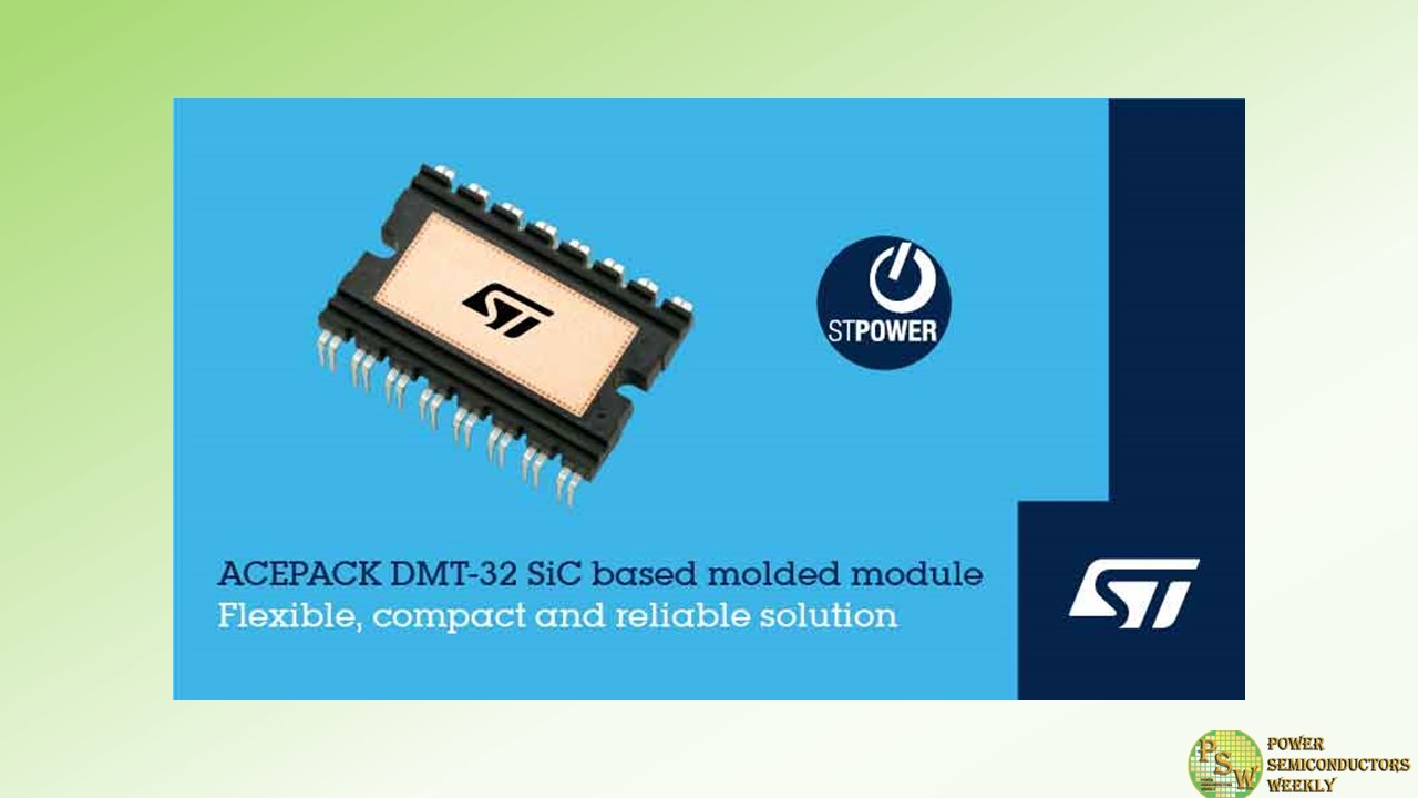
STMicroelectronics has released the ACEPACK DMT-32 family of silicon carbide (SiC) power modules in a convenient 32-pin, dual-inline, molded, through-hole package for automotive applications. Targeted at systems such as on-board chargers (OBC), DC/DC converters, fluid pumps and air conditioning, they deliver advantages including high power density, very compact design, and simplified assembly. The product family enhances flexibility for system designers by presenting a choice of four-pack, six-pack, and totem-pole configurations.
The modules contain 1200V SiC power switches that leverage ST’s state-of-the-art, second- and third-generation SiC MOSFET technology ensuring low RDS(on) values. The devices deliver efficient switching performance with minimal dependence on temperature to ensure high efficiency and reliability at converter system level.
Leveraging ST’s proven, robust ACEPACK technology, the modules reduce overall system- and design-development costs while ensuring outstanding reliability. The package technology features a high-performance aluminum nitride (AlN) insulated substrate for excellent thermal performance. There is also an integrated NTC sensor that provides temperature monitoring for thermal protection.
The first product in ACEPACK DMT-32, introduced today with ramp-up to volume production since Q4’23, is M1F45M12W2-1LA. The M1F80M12W2-1LA, M1TP80M12W2-2LA, M1P45M12W2-1LA, M1P80M12W2-1LA, M1P30M12W3-1LA are sampling now with ramp-up to volume production starting from Q1’24.
Original – STMicroelectronics
-
The Fraunhofer Institute for Solar Energy Systems ISE has developed and suc-cessfully commissioned the world’s first medium-voltage string inverter for large-scale power plants. By feeding power into the medium-voltage grid, the “MS-LeiKra” project team has demonstrated that PV inverters are technically capable of handling higher voltage levels.
The benefits for photovoltaics in-clude enormous cost and resource savings for passive components and cables. The device lays the foundation for a new system concept for the next genera-tion of large-scale PV power plants, which can also be applied to wind turbines, electric mobility and industrial applications.
Modern PV string inverters have an output voltage of between 400 VAC and 800 VAC. Although the output of power plants is steadily growing, voltage has not yet been increased. There are two reasons for this: First, building a highly efficient and compact inverter based on silicon semiconductors is a challenge. Second, there are currently no PV-specific standards that cover only the low-voltage range (max. 1,500 VDC / 1,000 VAC).
In a project funded by the German Federal Ministry for Economic Affairs and Climate Action (BMWK), Fraunhofer ISE, in collaboration with Siemens and Sumida, has developed an inverter that enables the output voltage to be increased to the medium-voltage range (1,500 V) at 250 kVA. The key to this is the use of silicon carbide semiconductors, which have a higher blocking voltage.
The research team has also implemented a more efficient cooling concept using heat pipes, which reduces the amount of aluminum required.
Thinner cables offer huge savings potential
An average photovoltaic power plant requires dozens of kilometers of copper cables. Increasing the voltage generates significant savings potential: At today’s possible output voltage of 800 VAC, a 250 kVA string inverter requires cables with a minimum cross section of 120 mm². By increasing the voltage to 1,500 VAC, the cable cross section can be reduced to 35 mm².
This in turn cuts copper consumption by around 700 kilograms per kilometer of cable. “Our resource analyses show that in the medium term, the electrification of the energy system will lead to copper becoming scarce. Increasing the voltage allows us to save valuable resources,” says Prof. Dr. Andreas Bett, Director of the Fraunhofer Institute for Solar Energy Systems ISE.
Standards need to change
With the “MS LeiKra” project, we are leaving the scope of low-voltage (<1000 VAC / <1500 VDC) standards. There are currently no PV-specific standards for this range. This is why the project team is also working on the standards that would result from increasing the voltage.
Finding a demo project partner
Having fed power into the medium-voltage grid successfully, the research team is now looking for solar farm developers and grid operators to test the power plant concept in the field.
Besides photovoltaics, moving beyond low voltage is also of interest for other applications, such as wind turbines, where the growing system capacities also require cables with large cross sections. The same is true for the charging infrastructure for large electric vehicles and vehicle fleets, and for industrial grids, where medium-voltage inverters could save a lot of material if cable cross sections could be reduced.
Original – Fraunhofer ISE
-

onsemi announced the completed expansion of its state-of-the-art, world-largest silicon carbide (SiC) fabrication facility in Bucheon, South Korea. At full capacity, this fab will be able to manufacture more than one million 200 mm SiC wafers per year.
To support the ramp in SiC manufacturing capacity, onsemi plans to hire up to 1,000 local employees over the next three years to fill the mostly highly technical positions – a more than 40% increase over the present workforce of about 2,300.
Silicon carbide devices are a critical component for power conversion in electric vehicles (EVs), energy infrastructure and high-power EV chargers. The rapidly growing demand for these products has created a surge in demand for SiC chips, with demand outpacing supply for the foreseeable future. The expansion of the Bucheon fab addresses the pressing need for additional production capacity, allowing onsemi to continue to provide supply assurance for its customers and strengthen its leadership in intelligent power solutions.
Construction of the new advanced 150 mm/200 mm SiC fab line along with the high-tech utility building and adjacent parking garage began in the middle of 2022 and was completed in September 2023. The expansion of the 150 mm/200 mm SiC Epi and wafer fab emphasizes onsemi’s focus on building out its vertically integrated silicon carbide manufacturing supply chain at brownfield locations. The Bucheon SiC line is starting with the production of 150 mm wafers and will be converted to 200 mm in 2025 upon qualification of the 200 mm SiC process.
onsemi’s leadership was joined by a delegation of dignitaries led by Vice Governor for Economy of the Gyeonggi-Do Taeyoung Yeom; followed by Bucheon City Mayor YongEek Cho; National Assembly delegates; and Bucheon Chamber of Commerce and Industry Chairman JongHuem Kim. Also in attendance were representatives from local communities, customers, suppliers and the semiconductor industry.
onsemi CEO Hassane El-Khoury opened the event, noting, “The 150 mm/200 mm SiC wafer fab in Bucheon is critical to the continued success of our fully integrated SiC supply chain, enabling us to support the acceleration of electrification globally. The last five years have shown what extraordinary performance our Bucheon team is capable of, and what we can achieve when we work together with governmental agencies toward the common goal of a more sustainable future.”
“I am truly impressed by onsemi’s diligent and yet fast execution of its strategic plan to expand the Bucheon SiC wafer fab,” said Bucheon City Mayor YongEek Cho. “Not only will the city of Bucheon benefit from the creation of new employment opportunities in technology, but it will also be a part of laying the foundation for a sustainable ecosystem through electrification.”
Original – onsemi
-
Navitas Semiconductor announced its continued sponsorship of the 2023 China Power Electronics and Energy Conversion Congress & the 26th China Power Supply Society (CPSS) Conference and Exhibition (CPSSC 2023), revealing major next-generation gallium nitride (GaN) and silicon carbide (SiC) power semiconductor platforms, including GaNSafe™ – the world’s safest GaN power semiconductor.
Hosted in Guangzhou from November 10th-13th, CPSSC 2023 celebrates its 40th anniversary and promotes academic and technical exchange in the fields of power electronics, energy conversion, and power technology, to foster technical innovation and related industries.
Navitas is the technology and market leader in GaN, with over 100 million GaNFast™ power ICs shipped, and over 12 million GeneSiC™ power MOSFETs and diodes shipped into a $22 billion per year total market opportunity.
With GaNSafe, Navitas has optimized its 4th-generation GaN technology for demanding, high-power applications in data centers, solar / energy storage and EV markets, where efficiency, power density and robust & reliable operation are critical. Adopting a novel, robust, and cool-running surface-mount TOLL package, GaNSafe integrates features and functions, including:
- Protected, regulated, integrated gate-drive control, with zero gate-source loop inductance for reliable high-speed 2 MHz switching to maximize power density.
- High-speed short-circuit protection, with autonomous ‘detect and protect’ within 50 ns – 4x faster than competing discrete solutions.
- Electrostatic discharge (ESD) protection of 2 kV, vs. zero for discrete GaN transistors.
- 650/ 800 V capability to aid survival during extraordinary application conditions.
- Easy-to-use, complete, high-power, high-reliability, high-performance power IC with only 4 pins, accelerating customer designs.
- Programmable turn-on and turn-off (dV/dt) to simplify EMI regulatory requirements.
Navitas’ CPSSC 2023 program includes comprehensive, in-depth technology, application and market presentations include a plenary keynote speech, full conference paper, four industrial sessions, a guest PSMA presentation, an in-depth 3.5-hour technology seminar and full GaNSafe launch. Visitors to the exhibition will discover ground-breaking technology demonstrations and complete power system platform designs at the Navitas booth.
Original – Navitas Semiconductor
-
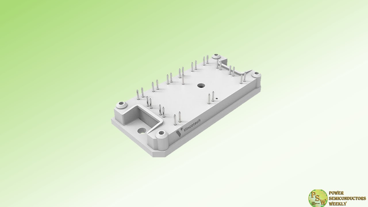
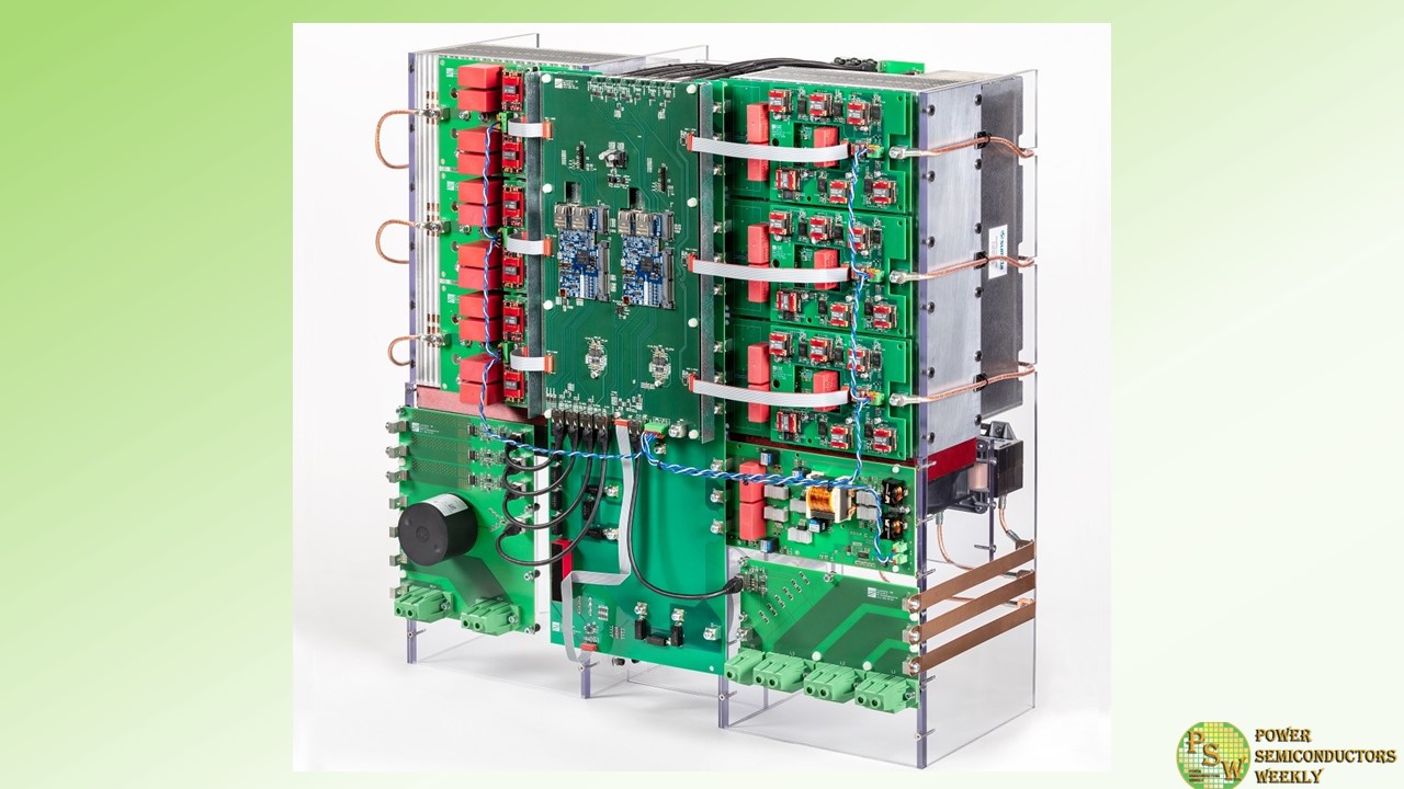
Designing state-of-the-art heat pumps and HVAC systems is not easy. Finding a way to overcome demands, such as giving more power in a smaller footprint requires a lot from a power module.
Vincotech’s new 1200 V PIM+PFC is the answer. Its integrated three-phase ANPFC and inverter stage resolve contradiction to boost efficiency and cut systems costs. More compact designs at higher power ranges is not a problem any more.
Samples are available through our usual channels.
Main benefits
- All-in-one solution: 3-phase PFC with inverter stage in a compact flow1 housing allows for more compact designs and higher power density
- High efficient AN-PFC topology with SiC diodes for switching frequencies up to 150 kHz reduces systems costs
- High speed IGBT’s in the inverter stage for high switching frequency operation
- Thin Al2O3 substrate eases the system’s thermal design
- Integrated thermal sensor simplifies temperature measurement
Applications
- Embedded drives
- Industrial drives
Original – Vincotech
-

Axcelis Technologies, Inc. announced the shipment of the Company’s Purion EXE SiC Power Series™ 200mm high energy implanter to a leading SiC power device chipmaker located in Japan. The system will be used in high volume production of SiC power devices for use in automotive applications.
Executive Vice President of Marketing and Applications, Greg Redinbo, commented, “The power device market is one of the fastest growing segments in IC manufacturing, due in part to the robust growth in the electric vehicles market. The power device market is at a critical inflection point as chipmakers transition from 150mm to 200mm SiC wafers.
The Purion Power Series family is uniquely suited to excel at these applications due to its innovative platform that offers the flexibility to handle multiple wafer sizes, various substrate types and operate at various implant temperatures. We look forward to continuing to expand the Purion platform footprint in Japan and supporting our customers’ goals to increase their manufacturing capacity.”
Original – Axcelis Technologies
-
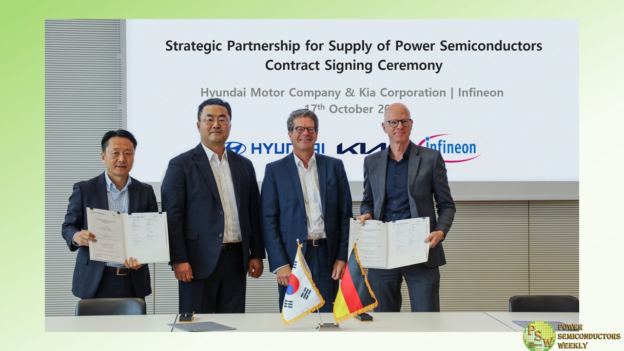
Infineon Technologies AG and Hyundai Motor Company and Kia Corporation have signed a multi-year supply agreement for silicon carbide (SiC) and silicon (Si) power semiconductors. Infineon will build and reserve manufacturing capacity to supply SiC as well as Si power modules and chips to Hyundai/Kia until 2030. Hyundai/Kia will support the capacity build-up and capacity reservation with financial contributions.
“Infineon stands as a valued strategic partner, boasting steadfast production capabilities and distinct technological prowess within the power semiconductor market,” said Heung Soo Kim, Executive Vice President and Head of Global Strategy Office (GSO) at Hyundai Motor Group. “This partnership not only empowers Hyundai Motor and Kia to stabilize its semiconductor supply but also positions us to solidify our leadership in the global EV market, underpinned by our competitive product lineups.”
“The future car will be clean, safe and smart and semiconductors are at the heart of this transformation. As a trusted partner, we are proud to advance our long-term partnership with Hyundai/Kia,” said Peter Schiefer, President of Infineon’s Automotive Division. “We contribute premium products of high quality, our system knowledge and application understanding combined with continued investments in manufacturing capacity to address the increasing demand for automotive power electronics.”
Infineon’s power semiconductors are key enablers for the transition to electromobility. This transition will lead to strong market growth for power semiconductors, especially those based on wide bandgap materials like SiC.
With the significant expansion of its Kulim fab, Infineon will build the world’s largest 200-millimeter SiC power fab and further strengthen its market-leading role as a high-quality, high-volume supplier to the automotive industry. In line with Infineon’s multi-site strategy, the Kulim facility will complement Infineon’s current manufacturing capacity in Villach, Austria, and further capacity expansions in Dresden, Germany.
Original – Infineon Technologies
-
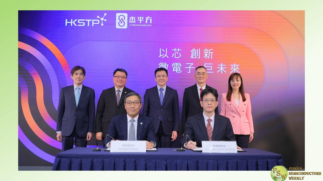
With support from the Innovation, Technology and Industry Bureau and the Office for Attracting Strategic Enterprises (OASES), the Hong Kong Science and Technology Parks Corporation (HKSTP) has signed a Memorandum of Understanding (MoU) with mainland China-based microelectronics enterprise J2 Semiconductor (Shanghai) Co. Ltd. (J2 Semiconductor), to set up a global research and development (R&D) Centre focusing on third-generation semiconductors at the Hong Kong Science Park, and to set up Hong Kong’s first Silicon Carbide (SiC) 8-inch advanced wafer fab.
This is a milestone moment in the government’s ambition to establish Hong Kong as a leading microelectronics hub in the region. This further promotes new industrialisation, a core for the Innovation, Technology and Industry Bureau which published its “Hong Kong Innovation and Technology Development Blueprint”, with a mission to develop strategically advanced manufacturing industries, such as microelectronics and semiconductors. As one of the world’s largest import and export markets for semiconductors, Hong Kong is at the heart of the Greater Bay Area which offers huge potential in becoming a key hub in the global semiconductor supply and value chain.
Professor Sun Dong, Secretary for Innovation, Technology and Industry, said “This collaboration between HKSTP and J2 Semiconductor to set up the Hong Kong’s first-ever large-scale semiconductor wafer fab, demonstrates the commitment of the HKSAR Government in taking the initiative to turn its ‘new industrialisation’ vision into action. J2 Semiconductor is proactively building up the capacity, quality and competitiveness of Hong Kong’s tech talent pool. The project will also drive the development of related industries, including semiconductor equipment manufacturers, material suppliers, testing service providers, to develop a complete ecosystem to reinforce Hong Kong’s position in the global semiconductor industry value chain.”
The collaboration between HKSTP and J2 Semiconductor is jointly supported by the Innovation, Technology and Industry Bureau and OASES with a view to sustain Hong Kong’s innovation and technology ecosystem and promote new industrialisation. The MoU was witnessed by Professor Sun Dong, Secretary of Innovation, Technology and Industry Bureau, Mr Philip Yung, Director-General of OASES, Ms Lillian Cheong, Under Secretary for Innovation, Technology and Industry, Dr Sunny Chai, Chairman of HKSTP and Dr Robert Tsu, Chairman of J2 Semiconductor. While Mr Albert Wong, CEO of HKSTP and Mr TY Chu, Co-CEO of J2 Semiconductor formally signed the MoU.
Dr Sunny Chai, Chairman of HKSTP said, “The plan of establishing J2 Semiconductor’s R&D Centre in the Science Park will promote Hong Kong’s R&D and advanced manufacturing capabilities of third-generation semiconductor devices. J2 Semiconductor brings the core technology and expertise to Hong Kong in advanced chip design, fabrication process and semiconductor product development, which is an important milestone in the development of microelectronics industry in Hong Kong. As one of Hong Kong’s flagship innovation and technology platforms, we provide high-quality infrastructure and facilities as well as a vast network of partners, which will continue to promote Hong Kong’s microelectronics R&D capabilities and strengthen Hong Kong’s position as an international I&T hub.”
Dr Robert Tsu, Chairman of J2 Semiconductor said, “I am very grateful for the level of attention and support from both the Innovation, Technology and Industry Bureau and HKSTP to this project. The MoU signing officially launches our third-generation semiconductor ‘SiC 8-inch advanced wafer fab’ project. J2 Semiconductor will invest an estimated HK$6.9 billion into the project, with plans to start volume production in the next couple of years, and reach annual production capacity of 240,000 SiC wafers in 2028, generating an annual production value of more than HK$11 billion and creating more than 700 job positions in Hong Kong. The project will assist in the early completion of the localisation of the new energy vehicle supply chain and drive the long-term development and prosperity of the semiconductor industry in Hong Kong.”
As a semiconductor chip design enterprise, J2 Semiconductor is committed to meeting the strong demand for domestically produced automotive chips from the China automotive industry. It mainly provides high-performance silicon carbide (SiC) devices with a focus on automotive, power conversion and communications. J2 Semiconductor’s superior SiC technology can be applied to relevant applications such as electric vehicles, as well as the related infrastructure such as charging stations, smart grids and energy storage.
HKSTP is committed to promoting Hong Kong’s new industrialisation mission and building a world-leading microelectronics ecosystem. HKSTP has established an extensive network of microelectronics hardware infrastructure, including Sensor Packaging and Integration Laboratory (Sensor Lab), Heterogenous Integration Lab (HI Lab) and the Hardware Lab, which can support the end-to-end process of design, prototyping and pilot production of chip-related equipment and systems as well as products. The Microelectronics Centre in Yuen Long Innovation Park is set to begin operation in 2024, supporting HKSTP’s infrastructure to accelerate microelectronics R&D pilot production, creating opportunities for upstream and downstream enterprises in the industry chain.
The microelectronics ecosystem of HKSTP is flourishing, with more than 200 microelectronics related companies. The establishment of the J2 Semiconductor facilities in Hong Kong will create greater level of synergy and knowledge exchange. Currently, five universities in Hong Kong are ranked among the top 100 universities in the world, with more than 100 university researchers engaged in microelectronics research, and promote the R&D of third-generation semiconductors. In this year’s Budget Speech, the HKSAR Government announced its plan to establish a Microelectronics Research and Development Institute to strengthen collaboration with universities, R&D centres and companies in the industry, and further accelerate the “1 to N” translation of R&D outcomes and bolster industry development.
Original – HKSTP
-
With decades of expertise in power device packaging and testing, JCET Group offers a comprehensive power product portfolio encompassing IGBT, SiC, GaN, and more. In the field of high-density power solutions for automotive applications, JCET’s unique power module technology positions us at the forefront of power main drive solutions.
JCET’s innovative packaging technology for high power density Silicon Carbide (SiC) power modules minimizes parasitic effects and thermal resistance, while our groundbreaking interconnect technology ensures high reliability. Reduced power loss and improved performance, making JCET the preferred choice for high-reliability SiC device packaging for the automotive industry.
The rapid growth of the power semiconductor market in automotive applications is being driven by the acceleration of vehicle electrification. In this evolving landscape, a multitude of power devices find applications in crucial automotive systems such as motor control, DC-DC conversion, air conditioning drives, on-board chargers (OBC), and battery management for electrical vehicles.
According to research by Strategy Analytics, the value of power devices in battery electric vehicles (BEVs) is nearly five times that in traditional fuel vehicles. This is where SiC devices come into play, offering several advantages. SiC devices feature smaller conductor resistors per unit area, higher voltage capabilities, faster switching speeds, and the ability to operate at high temperatures. These characteristics are instrumental in enhancing the power density of the inverter, ultimately leading to improved operational efficiency and extended mileage for electric vehicles under real-world conditions.
JCET combines low stray inductance package technology, advanced interconnect packaging technology, and cutting-edge thermal management solutions, tailoring our packaging processes to meet individual customer requirements. Within this package, a suite of integrated solutions, including the whole-silver sintering process, copper wire bonding, and single-side direct water cooling, is employed.
Furthermore, SiC devices, with their smaller footprint, increased power density, and higher breakdown voltage compared to conventional silicon-based power devices, are at the core of our packaging. When integrated into an 800V platform, SiC devices deliver substantial system advantages, enabling rapid charging and extended mileage. JCET’s unwavering commitment to optimizing packaging technology is evident in our High-Performance Device (HPD) package, which is continuously fine-tuned to excel in SiC high-frequency switching applications.
With the growing adoption of SiC devices across diverse sectors like automotive controllers, charging stations, and photovoltaic energy storage, JCET has pioneered innovative designs encompassing packaging materials, internal connections, and packaging structures. JCET has introduced a range of packaging solutions tailored to meet various user requirements, including:
- 400V platform, A0/A00 vehicles within 70KW: Si Hybrid Package1 solution;
- 400V platform, Class A vehicles between 100-200KW: Si/SiC Hybrid Package Driver solution;
- 800V platform, Class B and luxury cars with 200KW and above: SiC single/double sided heat dissipation solution.
Automotive power devices, including SiC, hold vast market potential and exhibit a high level of technical innovation certainty. This presents a compelling opportunity for device designers and manufacturers. Looking ahead, JCET remains committed to its core mission of advancing power device packaging solutions, We are dedicated to expanding our technology offerings, ensuring our customers have a diverse array of options, helping them integrate more efficient and reliable technologies into the new energy vehicle systems.
Original – JCET
