-

Magnachip Semiconductor Corporation announced the launch of two new 6th-generation (Gen6) 650V Insulated Gate Bipolar Transistors (IGBTs), specifically designed for solar inverters.
The newly introduced Gen6 IGBTs, incorporating polyimide insulation layers, demonstrate outstanding performance by passing high-voltage, high-humidity and high-temperature reverse bias (HV-H3TRB) tests. These products offer dependable reliability in industrial equipment operating under extreme conditions, including elevated temperatures and humidity.
Additionally, integrated fast recovery anti-parallel diodes ensure swift removal of residual current, reducing switching losses in applications while supporting an operating temperature range of up to 175°C.
Of the two new products, the MBQ40T65S6FHTH features exceptional conduction loss reduction. Compared to the previous generation, this IGBT decreases conduction loss by approximately 25% and boosts system efficiency by about 15% in 15kW solar inverters.
The MBQ40T65S6FSTH is engineered to significantly reduce switching loss. It cuts switching loss by 15% and conduction loss by approximately 8% compared to its predecessor, enhancing system efficiency by about 11% in 3kW solar inverters.
With these performance upgrades, the new IGBTs are suitable for applications that demand high reliability and efficiency, such as solar inverters, industrial motor drives, power supply units and uninterruptible power supplies.
According to market research firm Omdia, the discrete IGBT market in the renewable energy sector is expected to grow at a compound annual growth rate of 19% from 2025 to 2028.
“In the second half of this year, we plan to introduce a broader range of Gen6 650V IGBT products with current ratings from 5A to 75A, as part of our strategy to significantly expand our pipeline of new-generation Power products,” said YJ Kim, CEO of Magnachip. “We have a proven track record in Power with nearly 1,000 chip designs and the manufacture and shipment of more than 23 billion units since we entered the Power business in 2007. Moving forward, we will continue to strengthen our IGBT product family to drive innovation in renewable energy, automotive, industrial and AI applications.”
Original – Magnachip Semiconductor
-

Magnachip Semiconductor Corporation announced a significant expansion of its product lineup with the launch of 25 new 6th-generation (Gen6) SJ MOSFETs (Super Junction Metal-Oxide-Semiconductor Field-Effect Transistors).
The switching speeds of the newly developed Gen6 SJ MOSFETs have been improved by approximately 23%, reducing the RSP of applications by about 40% compared to the previous generation, thereby enhancing the Figure of Merit by 40%.
Additionally, a Zener diode is embedded between the gate and source to enhance reliability and protect the SJ MOSFETs from ESD-induced damage. The chip sizes of the new products are also approximately 30% smaller than their predecessor product.
The new product lineup consists of 600V, 650V, and 700V voltage ratings and is available in 7 package types, including TO220, TO220FT, SOT223, PDFN88, and D2PAK, with high-demand options, such as DPAK and TO220F.
As a result, these SJ MOSFETs are well-suited for various applications requiring high power efficiency, including AI TVs, smart refrigerators, AI laptop adapters and power supplies. According to market research firm Omdia, the global smart home device market is projected to grow by 20% annually from 2025 to 2028.
“With the successful launch of 25 new Gen6 SJ MOSFETs integrating Magnachip’s latest technology, we have further strengthened our product lineup to meet our customers’ evolving technical requirements,” said YJ Kim, CEO of Magnachip. “By delivering optimal power solutions for the AI, industrial applications and smart home appliances, we aim to contribute to the growth and success of our customers in these sectors, and further advance our technology and market leadership as we transition to a pure-play Power company.”
Original – Magnachip Semiconductor
-

Alpha and Omega Semiconductor Limited (AOS) announced the release of two state-of-the-art surface mounting package options for its industry-leading high power MOSFET portfolio. Designed to meet the robust packaging requirements for the most demanding applications that require increased performance and reliability, the new GTPAK™ and GLPAK™ packages will first be available on AOS’ AOGT66909 and AOGL66901 MOSFETs respectively. Combining AOS-proven robust MOSFET technology with advanced packaging know-how, these devices provide low ohmic and high current capabilities, critical to reducing the number of parallel MOSFETs needed in high current designs such as in next-generation e-mobility and industrial applications.
The GTPAK offered with the AOGT66909 is a topside cooling package designed with a large exposed pad for more efficient heat transfer. The topside cooling technology transfers most heat to the heat sink mounted on the top exposed pad. This feature allows the GTPAK to offer a more effective thermal dissipation route than going through the PCB board, allowing a lower-cost PCB, such as FR4, to be used.
The GLPAK offered with the AOGL66901 is a gull-wing version of AOS’ successful TOLL package. It is designed using AOS’ advanced clip technology to achieve a high inrush current rating. The GLPAK with clip technology offers very low package resistance and parasitic inductance, improving EMI performance compared to other package types that employ standard wire bonding.
The GTPAK and GLPAK packages feature gull-wing leads, enabling excellent solder joint reliability even for insulated metal substrates (IMS) applications. This gull-wing construction also provides enhanced thermal cycling for IMS boards and other critical applications that must meet higher reliability objectives. AOS MOSFETs in the new GTPAK and GLPAK packages are manufactured in IATF16949-certified facilities and are compatible with automated optical inspection (AOI) manufacturing requirements.
“We are committed to delivering new solutions to help our customers meet or exceed their power performance requirements. By offering our industry-leading MOSFETs in the new robust GTPAK and GLPAK packages, AOS allows designers to select from two state-of-the-art packaging technologies that offer significant performance improvements. Furthermore, the advanced technologies in our AOGT66909 and AOGL66901 MOSFETs will help simplify new designs by reducing the number of devices needed while also providing the necessary higher current capability that makes overall system cost savings possible,” said Peter H. Wilson, Marketing Sr. Director of MOSFET product line at AOS.
Technical Highlights
Continuous Drain
Current (A)Pulsed Drain
Current (A)RDS(ON) Max
(mOhms)Part Number Package VDS
(V)VGS
(±V)TJ
(°C)@25°C @100°C @25°C @10V AOGT66909 GTPAK 100 20 175 366 258 1464 1.5 AOGL66901 GLPAK 100 20 175 448 316 1790 1.25 Original – Alpha and Omega Semiconductor
-

Cambridge GaN Devices revealed more details about a solution that will enable the company to address EV powertrain applications over 100kW – a market worth over $10B – with its ICeGaN® gallium nitride (GaN) technology. Combo ICeGaN® combines smart ICeGaN HEMT ICs and IGBTs (Insulated-Gate Bipolar Transistors) in the same module or IPM, maximizing efficiency and offering a cost-effective alternative to expensive silicon carbide (SiC) solutions.
Dr GIORGIA LONGOBARDI | FOUNDER AND CEO, CGD
“Today, inverters for EV powertrains either use IGBTs which are low cost but inefficient at light load conditions, or SiC devices which are very efficient but also expensive. Our new Combo ICeGaN solution will revolutionise the EV industry by intelligently combining the benefits of GaN and silicon technologies, keeping cost low and maintaining the highest levels of efficiency which, of course, means faster charging and longer range. We are already working with Tier One automotive EV manufacturers and their supply chain partners to bring this technology advancement to the market.”The proprietary Combo ICeGaN approach uses the fact that ICeGaN and IGBT devices can be operated in a parallel architecture having similar drive voltage ranges (e.g. 0-20V) and excellent gate robustness. In operation, the ICeGaN switch is very efficient, with low conduction and low switching losses at relatively low currents (light load), while the IGBT is dominant at relatively high currents (towards full load or during surge conditions).
Combo ICeGaN also benefits from the high saturation currents and the avalanche clamping capability of IGBTs and the very efficient switching of ICeGaN. At higher temperatures, the bipolar component of the IGBT will start to conduct at lower on-state voltages, supplementing the loss of current in the ICeGaN. Conversely, at lower temperatures, ICeGaN will take more current. Sensing and protection functions are intelligently managed to optimally drive the Combo ICeGaN and enhance the Safe Operating Area (SOA) of both ICeGaN and IGBT devices.
ICeGaN technology allows EV engineers to enjoy GaN’s benefits in DC-to-DC converters, on-board chargers and potentially traction inverters. Combo ICeGaN further extends the benefits of CGD’s GaN technology into the rich 100kW+ traction inverter market. ICeGaN ICs have been proven to be very robust and IGBTs have a long and proven track record in traction and EV applications. Similar, proprietary parallel combinations of ICeGaN devices with SiC MOSFETs have also been proven by CGD, but Combo ICeGaN – which is now detailed in a published IEDM paper – is a far more economical solution. CGD expects to have working demos of Combo ICeGaN at the end of this year.
Prof. FLORIN UDREA | FOUNDER AND CTO, CGD
“Having worked for three decades in the field of power devices, this is the first time I have encountered such a beautifully complementary technology pairing. ICeGaN is extremely fast and a star performer at light load conditions while the IGBT brings great benefits during full load, surge conditions and at high temperatures. ICeGaN provides on-chip intelligence while the IGBT provides avalanche capability. They both embrace silicon substrates which come with cost, infrastructure and manufacturability advantages.”CGD will be exhibiting at APEC (Applied Power Electronics Conference and Exposition). For more details about Combo ICeGaN, visit Booth 2039 at the Georgia World Congress Center | Atlanta, GA | March 16-20, 2025.
Original – Cambridge GaN Devices
-

MCC Semi revealed the latest MOSFET designed to help engineers balance efficiency and thermal performance in high-power applications. The 150V MCTL4D0N15YH boasts a remarkably low on-resistance of 4mΩ, minimizing conduction losses for optimal efficiency.
Housed in a robust TOLL package, this component features advanced split-gate trench (SGT) technology and a junction-to-case thermal resistance of 0.39K/W for superior heat dissipation.
Equipped with an operating junction temperature capability of up to 175°C, this new MOSFET is the ideal solution for demanding applications, including battery management systems, motor drives, and DC-DC converters.
Offering versatility across multiple industries, MCTL4D0N15YH enhances system performance and longevity while reducing overall energy consumption.
Features & Benefits:
- SGT Technology: Ensures outstanding electrical performance and efficiency.
- Low On-Resistance (4mΩ): Minimizes power losses, enhancing system efficiency.
- Low Conduction Losses: Reduce energy waste, optimizing energy usage.
- Low Junction-to-Case Thermal Resistance (0.39K/W): Provides excellent heat dissipation capabilities.
- High Operating Junction Temperature (up to 175°C): Delivers reliability in high-temperature environments.
Original – Micro Commercial Components
-
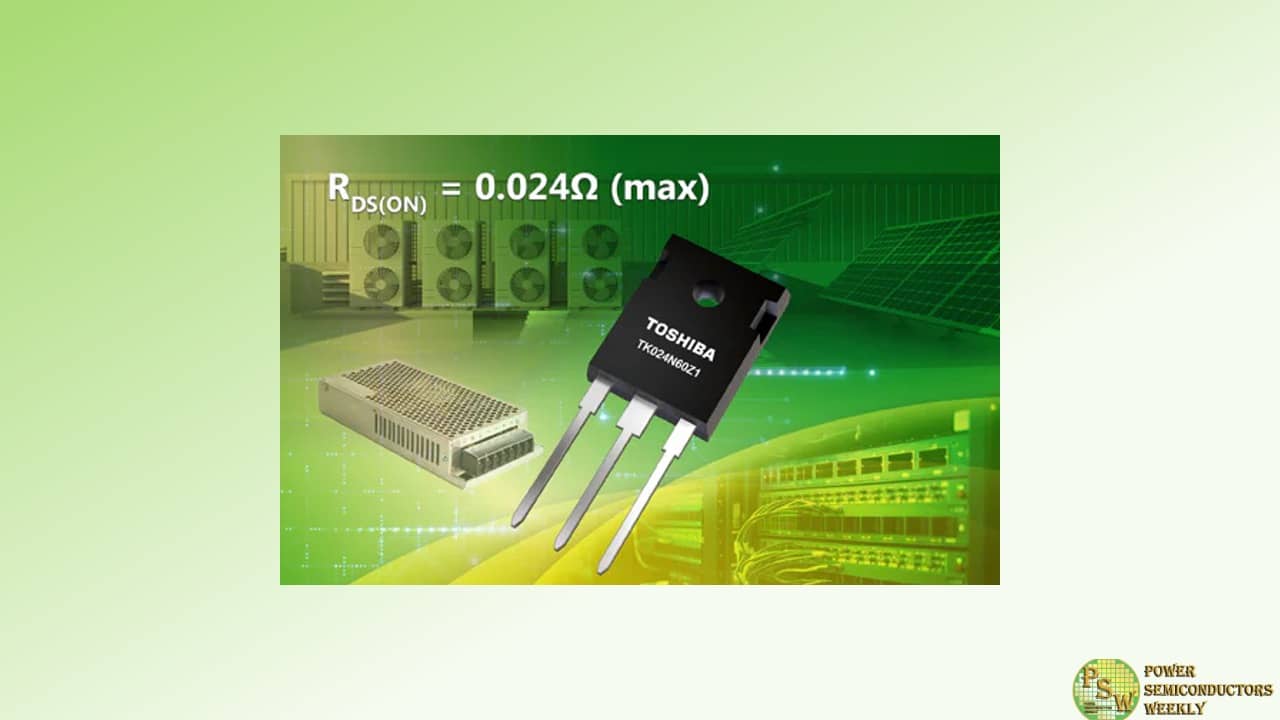
Toshiba Electronics Europe GmbH has launched an N-channel power MOSFET to address the growing market demand for improved efficiency in power supply circuits. The new TK024N60Z1 uses the proven DTMOSVI 600V series process with a super junction structure to achieve low on-resistance and reduced conduction losses. Applications include servers in data centres, switched-mode power supplies for industrial equipment, and power conditioners for photovoltaic generators.
The TK024N60Z1 has a drain-source on-resistance RDS(ON) of 0.024Ω (max), which is the lowest in the DTMOSVI 600V series. It also improves power supply efficiency, which reduces heat generation. Combined with the TO-247 package, which delivers high heat dissipation, the TK024N60Z1 offers good heat management characteristics.
Like other MOSFETS in the DTMOSVI 600V series, the TK024N60Z1 benefits from an optimised gate design and process. This reduces the value of drain-source on-resistance per unit area by approximately 13%. More importantly, drain-source on-resistance × gate-drain charge is reduced by approximately 52% compared to Toshiba’s conventional generation DTMOSIV-H series products with the same drain-source voltage rating. This means the DTMOSVI series, including the TK024N60Z1, offers a better trade-off between conduction loss and switching loss, which helps improve the efficiency of switched-mode power supplies.
To further improve power supply efficiency, Toshiba offers tools that support circuit design for switched-mode power supplies. These include the G0 SPICE model, which quickly verifies circuit function, and the highly accurate G2 SPICE models that reproduce transient characteristics.
The TK024N60Z1 N-channel power MOSFET exemplifies Toshiba’s commitment to continue expanding the DTMOSVI series and support energy conservation by reducing power loss in switched-mode power supplies.
Original – Toshiba
-

SUMCO Corporation announced plans to transfer wafer production from the Miyazaki Plant of consolidated subsidiary SUMCO TECHXIV Corporation to other manufacturing facilities, with the aim of improving profitability by reorganizing the production of silicon wafers of 200 mm and smaller.
The current silicon wafer market environment is in a prolonged sluggish demand phase, due to such factors as the drop-off from extraordinary demand during the COVID-19 pandemic, and structural changes in the semiconductor supply chain occasioned by US-China friction.
Drawdown of 300 mm wafer inventories by customers is taking time, as semiconductor production adjustments continue; but overall demand is expected to recover gradually thanks to strong needs for leadingedge products for AI semiconductors and high-performance memory. Demand remains sluggish, however, for small-diameter wafers mainly for consumer, industrial, and automotive uses. Wafers of 150 mm and smaller, in particular, are expected to see falling demand, with customers shifting to 200 mm wafers or lowering their production capacity as manufacturing equipment reaches its end of life.
In this market environment, the SUMCO Group has decided to reorganize the Miyazaki Plant to improve efficiency through consolidation of the production capacity of small wafers. The Miyazaki Plant will become a factory solely for monocrystalline production, while wafer production will be transferred to other domestic plants in the SUMCO Group and to Indonesia, ending wafer production in Miyazaki by the end of 2026.
SUMCO intends to reassign employees affected by the reorganization to 300 mm wafer operations after the end of wafer production in Miyazaki. With this reorganization, expenses for business structural reforms have been posted for fiscal 2024 as extraordinary losses totaling 5.8 billion yen, consisting of an impairment loss on non-current assets of 4.6 billion yen and an inventory write-down, etc., of 1.2 billion yen.
The SUMCO Group is committed to ongoing efficiency-raising initiatives, including reorganization of production facilities. Moreover, with the accelerating pace of innovation in semiconductor technology, in addition to strategically making use of advanced manufacturing equipment currently under preparation for operation, we will focus management resources on modernizing equipment in existing 300 mm plants and boost our capacity for supplying leading-edge products for AI with their remarkable growth, as we strive to further raise our corporate value.
Original – SUMCO
-

MCC Semi announced four new components in advanced P-channel MOSFET lineup. Supporting -100V applications from battery protection to motor drives and high-side switches, MCAC085P10, MCAC055P10, MCU055P10, and MCU085P10 are made for reliability in challenging environments.
With a maximum on-resistance of 55mΩ or 85mΩ, these MOSFETs improve overall system efficiency while reducing power dissipation. Leveraging trench technology and superior thermal performance, these versatile solutions provide engineers with high power density in a compact DFN5060 or DPAK package.
New P-channel MOSFETs are the obvious choice for unmatched performance and effective power management.
Features & Benefits:
- Trench MOSFET Technology: Enhances current capacity and reduces on-resistance
- Low On-Resistance: A maximum RDS(on) of 55mΩ or 85mΩ minimizes power consumption and boosts efficiency
- Low Conduction Losses: Reduce heat generation while improving overall system operation
- Excellent Thermal Performance: Safeguards device from overheating during use in high-temp scenarios
- High Power Density: Available in compact DFN5060 and DPAK package options
Original – Micro Commercial Components
-

Vincotech announced the release of flow E3BP, an advancement of the company’s widely adopted flow 2 and flow E3 housing. Engineered to meet the increasingly challenging requirements for next-gen systems, the flow E3BP is the next step up the evolutionary ladder in power module technology across applications.
Designed to boost thermal performance and maximize power density, this advanced housing is the go-to option for high-power systems and next-generation applications. Featuring a specially treated surface, its convex baseplate provides a superior thermal contact to better disperse heat and handle more power with a smaller footprint.
The module’s CTI600 housing material holds up well to higher system voltages. Its isolation walls increase creepage and clearance distances. Pre-applied thermal interface material is optionally available, as are Press-fit pins. Rolling efficiency, reliability, and innovation into one exceptionally useful housing, the new flow E3BP meets demand for faster time to market, higher power ratings, and greater power density. An excellent fit for many different applications, it marks another stride towards a more sustainable future.
Developed with the increasingly challenging demands of renewable energy systems in mind, the flow E3BP is a remarkably efficient power module. Among others, it enables customers to design 350+ kW utility string PV inverters with just a single housing per phase, cutting 30% of the cost for a dual-module solution. It also serves to reduce the heatsink area by as much as 34% compared to flow E3, thereby increasing power density to 51%.
Chosen for its low inductivity, the new flow E3BP figures prominently in solar and ESS inverters for the utility and commercial segments. Today’s flow E3BP housing meets tomorrow’s 2000 V systems’ high voltage requirements, and the company aims to extend this product portfolio to address further applications such as motion control, industrial drives, and EV charging stations.
Determined to enable customers to bring their ideas to life, Vincotech continues to develop its range of power module housings, which now encompasses 24 options rated from less than 10 kW up to MW. The flow 2, flow S3, and flow E3 housings see wide use in solar and ESS applications. The latest addition to the line, the leading-edge flow E3BP, supports beyond 350 kW and pushes the envelope for PV and ESS solutions.
Original – Vincotech
-

Mitsubishi Electric Corporation announced that it will begin shipping samples of two new S1-Series High Voltage Insulated Gate Bipolar Transistor (HVIGBT) modules, both rated at 1.7kV, for large industrial equipment such as railcars and DC power transmitters from December 26. Thanks to proprietary Insulated Gate Bipolar Transistor (IGBT) devices and insulation structures, the new modules offer excellent reliability and low power loss and thermal resistance, which are expected to increase the reliability and efficiency of inverters in large industrial equipment.
Mitsubishi Electric’s 1.7kV HVIGBT modules, first released in 1997 and highly regarded for their excellent performance and high reliability, have been widely adopted for inverters in power systems.
The new S1-Series modules incorporate Mitsubishi Electric’s proprietary Relaxed Field of Cathode (RFC) diode, which increases the Reverse Recovery Safe Operating Area (RRSOA) by 2.2 times compared to previous models for improved inverter reliability. In addition, the use of an IGBT element with a Carrier Stored Trench Gate Bipolar Transistor (CSTBT) structure helps reduce both power loss and thermal resistance for more efficient inverters.Furthermore, Mitsubishi Electric’s proprietary insulation structure increases the insulation voltage resistance to 6.0kVrms, 1.5 times that of previous products, resulting in more flexible insulation designs for compatibility with a wide range of inverter types.
Original – Mitsubishi Electric
