-

The University of Arkansas has taken the next step to becoming a national leader in the United States’ semiconductor economy. Semiconductors, such as silicon, are essential materials in most electronic devices and advance performance in fields such as healthcare, national defense, computing and transportation.
This August, the university began construction on the national Multi-User Silicon Carbide Research and Fabrication Facility, or MUSiC. Capable of silicon or silicon carbide chip fabrication, this new semiconductor research and fabrication facility will enable the government, businesses of all sizes, and universities to prototype in silicon carbide, introducing a capability that does not presently exist in the U.S.
This unique facility will offer low-volume prototyping for high-volume manufacturing, bridging the gap between traditional university research and the needs of private industry. This will accelerate both workforce development and technological advancement in semiconductors by providing a single location where chips can be go from developmental research to prototyping, testing and fabrication.
Alan Mantooth, Distinguished Professor of electrical engineering at the U of A, is principal investigator for MUSiC. He stated that with MUSiC, the university could “begin training the next generation at a variety of degree levels to provide well-trained and educated talent for onshoring semiconductor manufacturing that domestic suppliers offshored in the late 90s and early 2000s. Our training will be equally applicable to silicon and silicon carbide and other materials.”
Construction coincides with the CHIPS America Summit on Aug. 17, an invitation-only event for research, industry and governmental leaders from across the nation to discuss CHIPS and Science Act semiconductor-related opportunities and the ways in which the U of A and the State of Arkansas are uniquely positioned to lead.
The summit will feature Director of External and Government Affairs for the U.S Department of Commerce’s CHIPS Program Office, Adrienne Elrod. U.S. Representative Steve Womack and Arkansas Secretary of Commerce Hugh McDonald will also participate.
In addition to the MUSiC facility, the U of A is also home to the first Energy Frontier Research Center in Arkansas, as part of a team of researchers who received $10.35 million from the U.S. Department of Energy. The Center for Manipulation of Atomic Ordering for Manufacturing Semiconductors is dedicated to investigating the formation of atomic orders in semiconductor alloys and their effects on various physical properties. This research program will enable reliable, cost-effective and transformative manufacturing of semiconductors.
Researchers at the U of A previously established the MonArk NSF Quantum Foundry to accelerate the development of quantum materials and devices. In collaboration with Montana State University, and other member universities, the foundry supports the study of 2-D materials — consisting of a single layer of bonded atoms — by aiding researchers and facilitating the exchange of ideas across academia and industry. The project leads the fabrication of 2-D material quantum devices and their characterization, using low-temperature electronic transport and optoelectronic techniques.
The U of A’s existing and expanding research foundation means it’s uniquely positioned to take advantage of the recent CHIPS (Creating Helpful Incentives to Produce Semiconductors) and Science Act, which is providing approximately $280 billion in funding to stimulate domestic research and manufacturing of semiconductors.
As a result of manufacturing and production shortages of essential computer chips during the pandemic, which are overwhelmingly manufactured overseas, the federal government has prioritized the onshoring of this critical technology.
About the University of Arkansas: As Arkansas’ flagship institution, the U of A provides an internationally competitive education in more than 200 academic programs. Founded in 1871, the U of A contributes more than $2.2 billion to Arkansas’ economy through the teaching of new knowledge and skills, entrepreneurship and job development, discovery through research and creative activity while also providing training for professional disciplines.
The Carnegie Foundation classifies the U of A among the few U.S. colleges and universities with the highest level of research activity. U.S. News & World Report ranks the U of A among the top public universities in the nation. See how the U of A works to build a better world at Arkansas Research and Economic Development News.
The national Multi-User Silicon Carbide Research and Fabrication Facility, or MUSiC, will provide opportunities for the government and business of all sizes, and universities to prototype in silicon carbide, introducting a capability that does not currently exist in the U.S.
Original – University of Arkansas
-
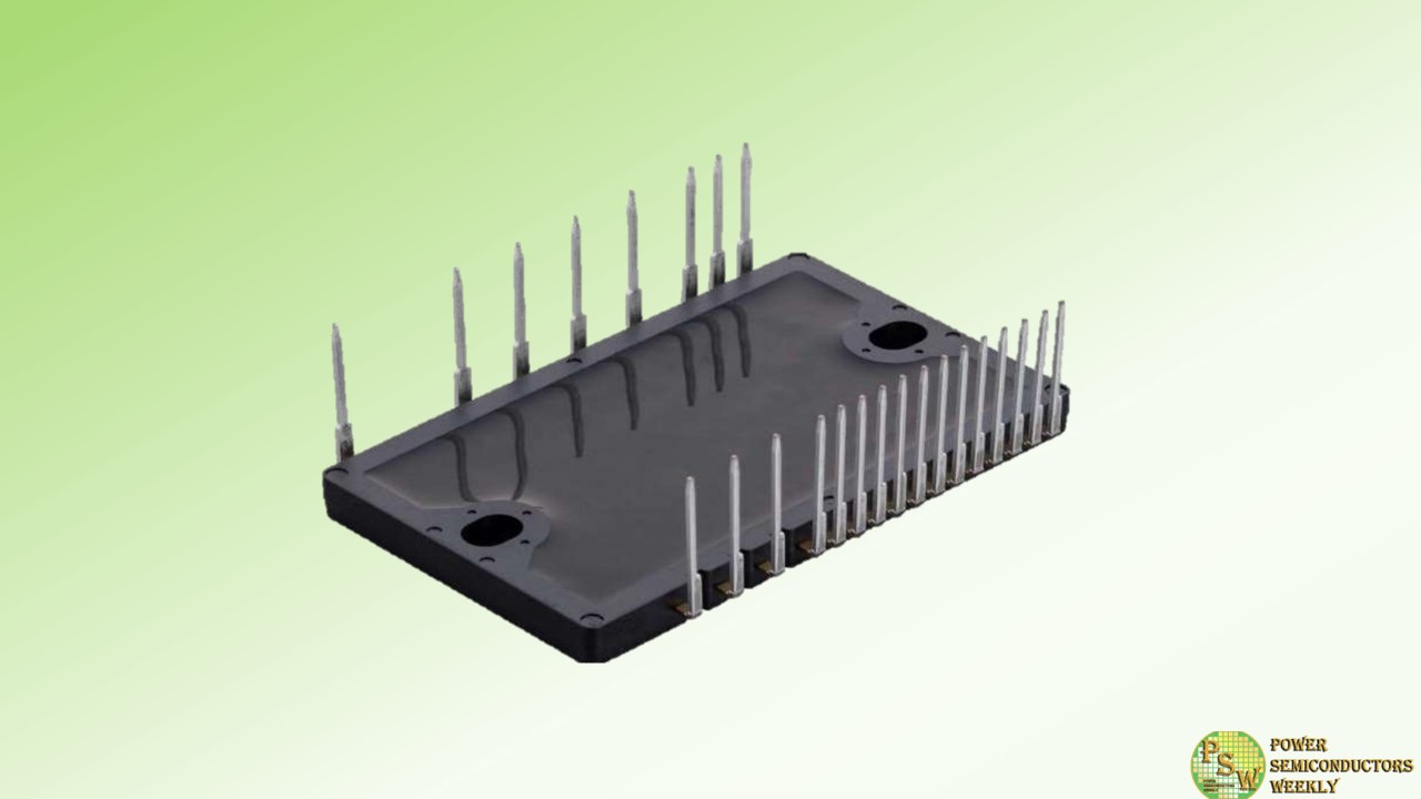
Fuji Electric Co., Ltd. announced the launch of the P633C Series 3rd-generation small IPMs, which help reduce the power consumption of the equipment on which it is mounted, such as home appliances and machine tools.
IPMs (intelligent power modules) are power semiconductors equipped with a built-in IGBT drive circuit and protection function. They are used for applications including inverters and servo systems. Inverters and servo systems control machine operation by controlling voltage and frequency through power semiconductor switching (turning electricity on and off), but power semiconductors generate power loss and electromagnetic noise during switching.
This product can reduce both the power loss and the electromagnetic noise generated during switching. Using this product in inverters for home appliances or servo systems for machine tools can reduce the power consumption of the equipment on which it is mounted, thereby contributing to the achievement of a decarbonized society.
One way to reduce the power loss that occurs during switching is to speed up the switching operation. Faster switching increases electromagnetic noise, which can cause peripheral devices to malfunction. This product uses the latest 7th-generation IGBT/FWD chips, achieving a 10% reduction of power loss and a reduction of electromagnetic noise to approximately 1/3 compared with conventional products. The trade-off characteristics between power loss and noise are among the best in the industry.
Original – Fuji Electric
-
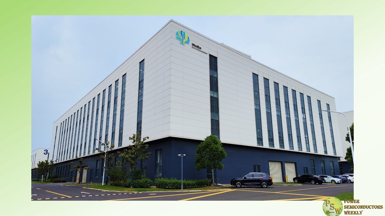
The opening ceremony of WeEnwin Jinshan Module Plant was held in the Shanghai Jinshan High-tech Industrial Development Zone. The ceremony marked the official commencement of WeEn’s world-first module plant, intended to produce various types of power module products utilized in consumer electronics, communications, new energy, and automotive applications. The products connect customers and the ecosystems, actively fostering the high-quality development of the industry.
Markus Mosen, WeEn Semiconductors Co., Ltd. CEO; Chen Song, COO; Tang Ziming, CFO; Wu Rui, CHRO; Peng Xijun, general manager of Shanghai New Jinshan Industrial Investment & Development Co., Ltd; Zhao Fei, deputy director of the Jinshan District Development and Reform Commission; Cao Qin, deputy director of the Jinshan District Investment Promotion Office; other relevant department heads of the New Jinshan Development Company; WeEn boards Zhang Xinyu, Chang Liang, and Zhu Fenglin; together with representatives from WeEn’s global partners, numerous customers, vendors, approximately 200 guests attended the event to personally witness this historic step in WeEn’s new journey.
Located in the Shanghai Bay Area High-tech Industrial and Development Zone, WeEn Jinshan Module Plant covers an area of 11,000 square meters. The construction of the plant began in August 2022. Eight months later in April 2023, the building quality and fire inspection compliance tests were successfully completed.
WeEn Semiconductors Co., Ltd. has invested approximately RMB 200 million in the wholly-owned new Jinshan Module Plant, which has introduced over a hundred of the industry’s most advanced power module production and testing equipment to meet the market’s mainstream demand for various types of module products.
It is worth underscoring that the newly established WeEnwin Module Plant has simultaneously set up an advanced packaging R&D center to develop and mass produce cutting-edge packaging technologies while researching the applicability of new materials.
To optimize efficiency and reliability, the fully automated module production line is equipped with top-notch processing capabilities, including lead-free chip bonding/silver sintering bonding, lead-free soldering/ultrasonic soldering of terminals, aluminum wire bonding, and copper tab connections. Currently, WeEnwin module plant. has obtained ISO9001 and IATF16949 certifications and undergone VDA6.3 process audits, evidence of the company’s robust system that guarantees top-quality products.
Peng Xijun, general manager of Shanghai New Jinshan Industrial Investment & Development Co., Ltd, warmly congratulated WeEnwin for the opening, noting that the event was a testimony of the concerted efforts of all parties. He further stated that the collective endeavors have significant importance in elevating the power semiconductor industry’s development level and accelerating the concentration of the optoelectronic chip industry in the high-tech industrial and development zone.
In addition, he expressed his wish for the high-tech zone, as it embarks on its new era journey, to continue harnessing resources and efforts and attracting policies aimed at strengthening the innovation chain, extending the industrial chain, and improving the ecosystem.
Meanwhile, Markus Mosen, WeEn Semiconductors Co., Ltd. CEO stated, “Given the favorable winds, this is the perfect time to set sail.” WeEn’s investment in the world’s first module factory has successfully transitioned from planning to operation according to schedule. Therefore, we remain grateful for the strong support from the Jinshan District People’s Government, Shanghai Bay Area High-tech Industrial Development Zone, and FITA Tech.
There is no doubt that without the collective efforts of our partners and team, this accomplishment would not have been possible. At WeEnwin, we will seize the opportunities of the era, leverage our product and technological strengths, and provide reliable and efficient power semiconductor devices to our customers and partners. As we inject new impetus into pragmatic cooperation, we remain confident in our ability to propel the ship of power device development toward a new journey.”
The operation of the WeEnwin Jinshan Module plant will enhance the efficiency of WeEn Semiconductors Co., Ltd.’s entire industry chain layout and services. In addition to producing the most advanced SCR / FRD / IGBT / SIC modules, the factory will significantly improve the experience of customers and partners by offering innovative modules and packaging services for the automotive and renewable energy markets. It is projected that the first batch of products from the new Jinshan Module Factory for Chinese and overseas customers will be shipped in the fourth quarter of 2023.
Original – WeEn Semiconductors
-
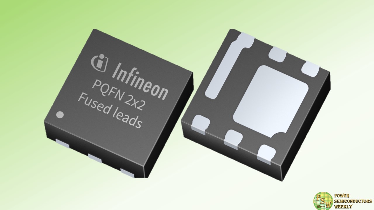
A small footprint of discrete power MOSFETs plays a critical role in achieving space savings, cost reduction, and easy-to-design applications. Additionally, higher power density can lead to layout routing flexibility and overall system size reduction. By expanding the current PQFN 2×2 portfolio with the new best-in-class OptiMOS™ power MOSFETs, Infineon Technologies AG offers benchmark solutions optimized for efficiency and performance in a small footprint. The new products are ideal for applications like synchronous rectification in switched mode power supplies (SMPS) for servers, telecom, and portable- and wireless chargers. Additional applications also include electric speed controllers for small brushless motors in drones.
The new OptiMOS 6 40 V and OptiMOS 5 25 V and 30 V power MOSFETs further optimize the proven OptiMOS technology for high-performance designs. They offer leading-edge silicon technology, package reliability, and superior thermal resistance (R thJC, max = 3.2 K/W) in the ultra-small PQFN 2×2 mm² package. The new devices combine industry-leading low on-resistance R DS(on) with industry-leading figures of merit (FOMs, Q G and Q OSS) for outstanding dynamic switching performance. As a result, MOSFETs with ultra-low switching and reduced conduction losses ensure optimal energy efficiency and power density, all while simplifying thermal management.
With the compact PQFN 2×2 mm² package outline, the OptiMOS power switches enable an improved system form factor with smaller, more flexible geometric outlines for end-user applications. The MOSFETs facilitate reliable system design with less need for paralleling, significantly reducing space and system cost.
Original – Infineon Technologies
-
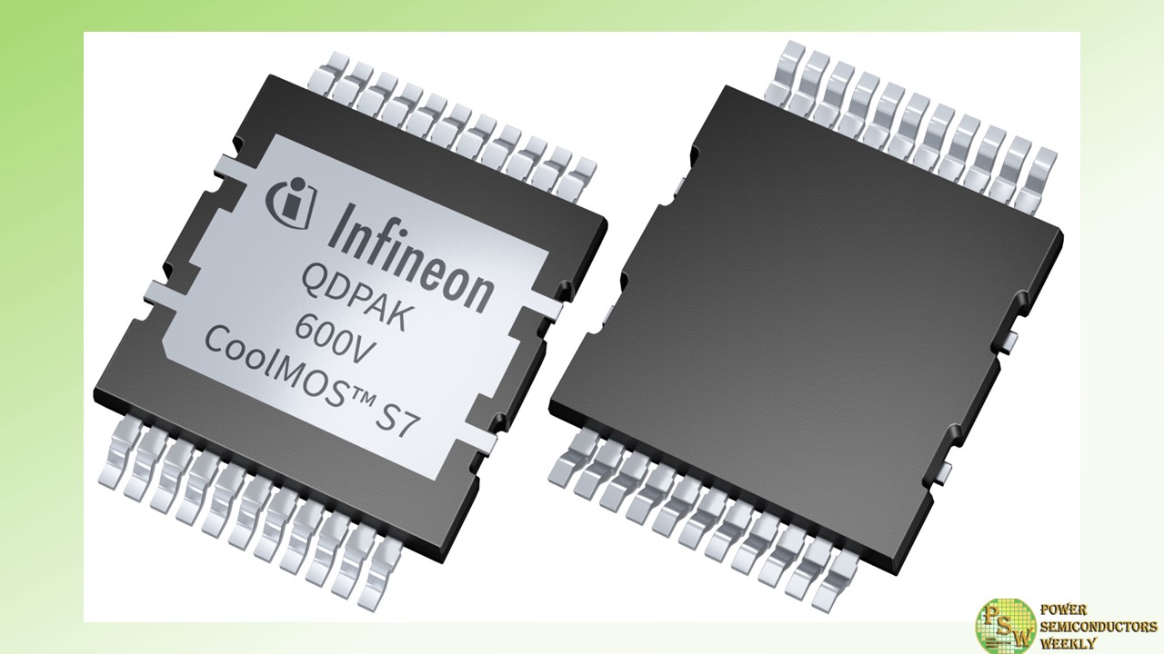
In static switching applications, power designs focus on minimizing conduction losses, optimizing thermal behavior, and achieving compact and lightweight systems while ensuring high quality at a low cost. To meet the needs of next-generation solutions, Infineon Technologies AG is expanding its CoolMOS™ S7 family of high-voltage superjunction (SJ) MOSFETs.
The devices are aiming at SMPS, solar energy systems, battery protection, solid-state relays (SSR), motor-starters and solid-state circuit breakers, as well as PLCs, lighting control, HV eFuse/eDisconnect, (H)EV on-board chargers.
The portfolio extension includes innovative QDPAK top-side cooling (TSC) packages and offers a wide range of features in a small footprint. This makes it highly advantageous for low-frequency switching applications while optimizing cost positioning.
Thanks to the novel high-power QDPAK packaging, they offer an R DS(on) of only 10 mΩ, which is the lowest on the market in this voltage class and the lowest in SMD packages. By minimizing conduction losses of the MOSFETs, the CoolMOS S7/S7A solutions contribute to higher overall efficiency and provide an easy and cost-optimized way to improve system performance.
The CoolMOS S7 power switches also effectively manage heat dissipation with improved thermal resistance. Thanks to the innovative and efficient QDPAK packaging, they also reduce or even eliminate the need for heat sinks in solid-state designs, resulting in more compact and lighter systems.
The MOSFETs are available in both top-side and bottom-side variants, and feature high-pulse current capability, enabling them to handle sudden surges of current. In addition, they exhibit body diode robustness to ensure reliable operation during AC line commutation.
With fewer components required, they reduce part count, resulting in flexible system integration, lower BOM costs, and total cost of ownership (TCO). In addition, these MOSFETs enable shorter reaction times, particularly when breaking a current, facilitating smoother and more efficient operation.
Original – Infineon Technologies
-
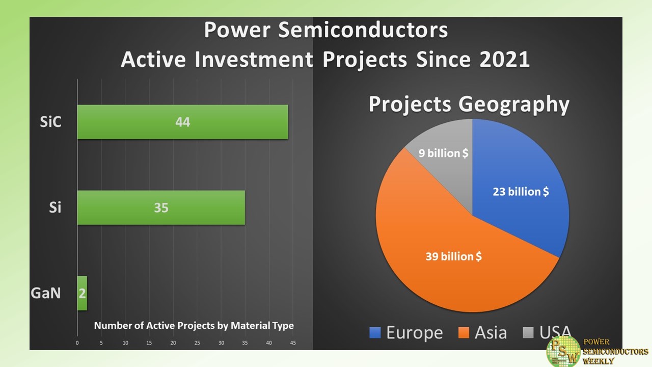
Power semiconductors companies continue to invest heavily in new factories, production capacity expansions, and R&D centers. Thus, recently the total value of the active investment projects launched since 2021 has surpassed 70 billion USD.
Driven by the pandemic and geopolitics, major power semiconductors companies started to invest more in new factories and joint ventures to have more confidence in their own supply chain in the future.
As of today, it is obvious to see the major split of power semiconductors into three geographical regions – the USA, Europe, and Asia. Asia may as well be divided into several regions with China being the leading investor of all.
Despite the ongoing tensions and export restrictions between the US, Europe, and China related to advanced semiconductors, when it comes to power semiconductors European companies continue to invest in the Chinese market expanding their product capacity or establishing new joint ventures like STMicroelectronics and Sanan Optoelectronics did recently.
Even with some delay, Japanese companies like ROHM, Mitsubishi Electric, Fuji Electric, Renesas Electronics, Toshiba, and others, pushed by their US and European competitors, announced their own projects aimed to secure the capacity on the wafer and device level to correspond to the growing demand for Si and SiC based power semiconductors coming from the electric vehicle and charging, photovoltaics, battery energy storage systems, and the other emerging applications.
If we take a closer look at all projects announced, SiC is the leading technology with over 60% of total investment. Over 25 market leaders announced their plans to invest in silicon carbide.
Thus, ROHM is investing in new production to multiply its SiC capacity in the coming years. Mitsubishi Electric teams up with Coherent to scale manufacturing of SiC power devices on a 200 mm SiC technology platform as one of the steps of their 260 billion yen investment project planned till March 2026.
Infineon Technologies continues to bet on both local European and Asian markets investing in their new fab in Dresden and expanding backend operations in Indonesia. STMicroelectronics continues to invest in WBG semiconductors with the ongoing construction of a new wafer fab in Sicily announced in 2022.
With a global total number of new investment projects of over 80, the US companies Wolfspeed, onsemi, and Microchip Technology, similar to their European counterparts, invest locally, in Europe and Asian markets. Totally the US semiconductor companies announced new projects valued at almost 9 billion USD.
With the US and EU Chips Acts, and similar initiatives in China, Japan, South Korea, and some other countries, it is clear that the investment into power semiconductors industry will continue to reach 100 billion USD soon.
-

Semiconductors are the linchpin to the performance, safety, and customer features of Stellantis vehicles today and in the new state-of-the-art, BEV-centric STLA vehicle and technology platforms arriving soon. As the auto industry’s demand for semiconductors accelerates, Stellantis is implementing a multifaceted strategy designed to manage and secure the long-term supply of vital microchips. Developed by a cross-functional team, the strategy was created through a rigorous assessment of customer desires for advanced technology features and a keen focus on delivering the objectives laid out in the Stellantis Dare Forward 2030 plan.
The robust strategy, which is refined continuously, includes:
- implementation of a semiconductor database to provide full transparency on the semiconductor content;
- systematic risk assessment to avoid and proactively remove legacy parts;
- long-term chip level demand forecasting to support capacity securitization agreements with chip makers and Silicon Foundries;
- implementation and enforcement of a Green List to reduce chip diversity and – in case of future chip shortages – to put Stellantis in control of the allocation; and,
- the purchasing of mission-critical parts at chip makers including a long-term securitization of chip supply.
Stellantis has started to engage with strategic semiconductor providers like Infineon, NXP® Semiconductors, onsemi, and Qualcomm to further improve its all-new, state-of-the-art STLA platforms and technologies. In addition, Stellantis is working with aiMotive and SiliconAuto to develop its own differentiating semiconductors in the future.
“An effective semiconductor strategy requires a deep understanding of semiconductors and the semiconductor industry,” said Maxime Picat, Chief Purchasing and Supply Chain Officer at Stellantis. “We have hundreds of very different semiconductors in our cars.
We have built a comprehensive ecosystem to mitigate the risk that one missing chip can stop our lines. At the same time, key vehicle capabilities directly depend on the innovation and performance of single devices. SiC MOSFETS extend the range of our electric vehicles while the computation performance of a leading-edge SoC is essential for the customer experience and safety.”
To date, Stellantis has entered into direct agreements for semiconductors with a purchasing value of more than €10 billion through 2030. The supply agreements cover a variety of vital microchips, including:
- Silicon Carbide (SiC) MOSFETS, which are fundamental to the range of EVs.
- Microcontroller Unit (MCU), a key part of the computing zones for the STLA Brain electrical architecture.
- System-on-a-chip (SoC), where performance is essential for the high-performance computing (HPC) units that deliver the in-vehicle infotainment and autonomous driving assist functions.
Semiconductors play key roles in the vehicles that are driving the Stellantis transformation into a sustainable mobility tech company, as outlined in Dare Forward 2030. This includes enabling features and functions in the BEV-native STLA global platforms (Small/Medium/Large/Frame) and the seamless connectivity, remote upgradability, and the flexible service-oriented electrical/electronic architecture that underpins the STLA Brain, STLA SmartCockpit, and STLA AutoDrive artificial intelligence-powered platforms.
Original – Stellantis
-
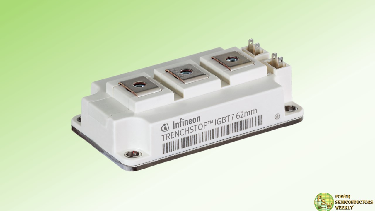
Infineon Technologies AG introduced a 62mm half-bridge and common emitter module portfolio with 1200 V TRENCHSTOP™ IGBT7 chips. The wide range of offerings in the proven 62mm housing is extended with the new 800 A maximum current class for the package family. The addition to the portfolio’s current classes provides system designers with a high degree of flexibility in designing higher current power solutions while offering higher power density and electrical performance.
It is tailored to meet the needs of solar central inverters as well as industrial drive applications and uninterruptible power supplies (UPS). Additionally, EV charging, energy storage systems (ESS) and other new industrial applications can be covered.
Based on the new micro-pattern trench technology, the 62mm module family with the 1200 V TRENCHSTOP IGBT7 chip has significantly lower static losses compared to the modules with the IGBT4 chipset. This results in significant loss reduction in applications, especially in industrial drives that typically operate at moderate switching frequencies. The IGBT’s oscillation behavior and controllability have been improved. In addition, the new power modules feature a maximum overload junction temperature of 175°C.
A solid, nickel-coated copper baseplate and screw main terminals ensure the high mechanical robustness of the 62mm module housing. The main terminals are located in the center of the housing, making them well suited for parallel circuits and 3-level configurations due to the low inductive DC link connection.
Unchanged standard package design and dimensions within the module family support mechanical compatibility with the previous module version. In addition, all modules are available with Infineon’s proven pre-applied thermal interface material (TIM).
Original – Infineon Technologies
-

Cars with fully or partially electrified drivetrains will account for two thirds of cars produced by 2028, as per analyst forecasts. This rapid growth of electromobility is driving the demand for power semiconductors. Against this background, Infineon Technologies AG and Semikron Danfoss have signed a multi-year volume agreement for the supply of silicon-based electromobility chips.
Infineon will supply chipsets consisting of IGBTs and diodes to Semikron Danfoss. These chips are mainly used in power modules for inverters, which are used for the main drive in electric vehicles.
“As the global leader in automotive semiconductors, Infineon enables game-changing solutions for clean and safe mobility. Already today, our IGBTs and diodes play a major role in the industry’s electromobility transformation by enabling efficient power conversion in the electric powertrain,” said Peter Schiefer, President of Infineon’s Automotive division. “Our broad product portfolio, system expertise and continuous investment in our manufacturing capabilities make us a valued partner of automotive players like Semikron Danfoss.”
Claus A. Petersen, President of Semikron Danfoss added: “Semikron Danfoss provides automotive customers with power modules based on the most advanced assembly technologies that fully exploit the capabilities of IGBTs and diodes to enable further decarbonization of the transportation sector. Automotive customers trust us as an experienced long-term partner to drive the transformation in the industry.”
The IGBTs and diodes for Semikron Danfoss will be manufactured by Infineon at its sites in Dresden, Germany, and Kulim, Malaysia. Semikron Danfoss manufactures its own automotive power modules in Nuremberg and Flensburg in Germany, in Utica, US, and as of next year, in Nanjing, China.
Original – Semikron Danfoss
-
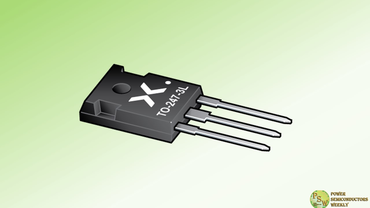
Nexperia launched its entry to the insulated gate bipolar transistor (IGBT) market with a range of 600 V devices, starting with the 30A NGW30T60M3DF. By adding IGBTs to its extensive portfolio, Nexperia is addressing the growing demand for efficient, high-voltage switching devices with a range of performance and cost requirements.
These enable higher power density in power conversion and motor drive applications, including industrial motor drives like servo motors ranging from 5 to 20 kW (20 kHz), robotics, elevators, operating grippers, in-line manufacturing, power inverters, uninterruptible power supply (UPS), photovoltaic (PV) strings, EV-charging, and induction heating and welding.
IGBT is a relatively mature technology. Nonetheless, the market for these devices is expected to grow in line with the increased adoption of solar panels and electric vehicle (EV) chargers. Nexperia’s 600 V IGBTs feature a robust, cost-effective carrier-stored trench-gate advanced field-stop (FS) construction, providing exceptionally low conduction and switching loss performance with high levels of ruggedness in operating temperatures up to 175°C. This improves the efficiency and reliability of power inverters, induction heaters, welding equipment and industrial applications like motor drives and servos, robotics, elevators, operating grippers, and in-line manufacturing.
Designers can choose between the medium speed (M3) and high speed (H3) series IGBTs. These IGBTs have been designed with very tight parameter distributions, allowing multiple devices to connect safely in parallel. In addition, lower thermal resistance than competing devices enables them to provide higher output power. These IGBTs are also fully rated as soft fast reverse-recovery diodes. This means they are suitable for rectifier and bi-directional circuit applications or to protect against overcurrent conditions.
“With the release of these IGBTs, Nexperia provides designers with a greater choice of power-switching devices for a broad range of power applications”, according to Dr. Ke Jiang, General Manager Business Group Insulated-Gate Bipolar Transistors & Modules at Nexperia. “IGBTs are the ideal complement to Nexperia’s existing range of CMOS and wide-bandgap switching devices, making Nexperia a one-stop-shop for power electronics designers.”
These IGBTs are available in a standard, lead-free, TO247-3L package and are HV-H3TRB qualified for outdoor applications. Nexperia plans to follow this release with a series of 1200 V IGBTs. To learn more about Nexperia’s IGBTs, visit: https://www.nexperia.com/igbts
Original – Nexperia
