-
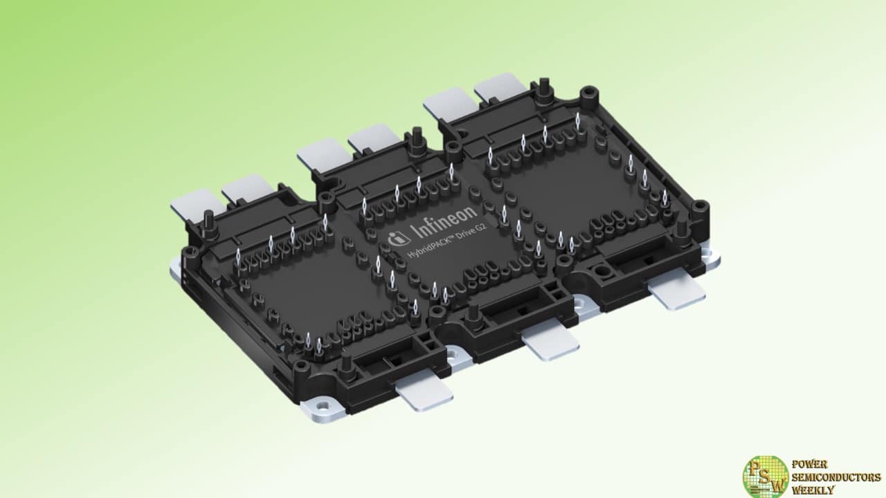
Infineon Technologies AG will supply Rivian’s R2 platform with power modules for traction inverters. The R2 platform will use silicon carbide (SiC) and silicon (Si) modules from Infineon’s HybridPACK™ Drive G2 family. Supply is expected to start in 2026. Additionally, Infineon will supply other products for the platform, including AURIX™ TC3x microcontrollers and power management ICs.
“We are committed to enhancing the performance and range of electric vehicles jointly with innovative automotive companies like Rivian,” said Stefan Obersriebnig, head of the product line for high voltage modules in Infineon’s Automotive Division. “Our dedication for innovation and zero-defect quality has made us the preferred partner of the automotive industry. With our broad product portfolio, system expertise and manufacturing capabilities, we are a key enabler of emission-free, sustainable mobility.”
HybridPACK Drive is Infineon’s market-leading power module family for electric vehicles. With more than 10.5 million units sold since 2017, it contributes significantly to the transition to electromobility. This transition will lead to strong market growth for power semiconductors, especially those based on wide bandgap materials like SiC.
With the expansion of its Kulim fab, Infineon is building the world’s most competitive 200-millimeter SiC power fab and further strengthens its market-leading role as a high-quality, high-volume supplier to the automotive industry. As “Infineon One Virtual Fab” for highly innovative wide bandgap (WBG) technologies, Infineon’s production sites in Kulim and Villach share technologies and processes. This allows for fast ramping and smooth and highly efficient operations in SiC and gallium nitride (GaN) manufacturing and reinforces Infineon’s technological leadership across the spectrum of all power semiconductor materials, in silicon as well as SiC and GaN.
Original – Infineon Technologies
-

Alpha and Omega Semiconductor Limited (AOS) announced its AOTL66935 utilizes AOS’ 100V AlphaSGT™ proprietary MOSFET technology which combines the advantages of trench technology for low on-resistance with high safe operating area (SOA) capability that meets 48V hot swap requirements in AI server and telecom applications.
The AOTL66935 hot swap MOSFET prevents damage to the system by limiting the high inrush current with low power losses due to the very low on-resistance (RDS(ON)). These features help deliver increased performance and reliability in harsh application conditions required in latest AI server designs. The AOTL66935 is available in TO-Leadless (TOLL) package, which is 30% smaller footprint compared to TO-263 (D2PAK). AOTL66935 is manufactured in IATF 16949-certified facilities. TOLL package technology is compatible with automated optical inspection (AOI) manufacturing requirements.
“48V hot swap in AI servers requires a MOSFET that excels in high current capability while providing exceptional SOA robustness with high reliability. We designed the AOTL66935 to meet these demands, and the low on-resistance reduces the power losses and can enable less devices in parallel,” said Peter H. Wilson, Sr. Director of MOSFET product line at AOS.
Technical Highlights
Part Number Package VDS (V) VGS (±V) TJ (°C) Continuous Drain Current (A) Pulsed Drain Current (A) RDS(ON) Max (mOhms) @10V @25°C @100°C @25°C AOTL66935 TOLL 100 20 175 360 258 1440 1.95 Pricing and Availability
The AOTL66935 MOSFET is immediately available in production quantities with a lead time of 14-16 weeks. The unit price in 1,000-piece quantities is $4.2.
Original – Alpha and Omega Semiconductor
-

Infineon Technologies AG provides its 600 V CoolMOS™ 8 high-voltage superjunction (SJ) MOSFET product family to LITEON, a leader in power management solutions, for superior efficiency and reliability in server applications. The 600 V CoolMOS 8 offers an all-in-one solution that improves LITEON’s new generation technology for existing and upcoming server application designs.
Infineon’s newest CoolMOS 8 at 600 V is leading the way in high-voltage superjunction MOSFET technology, setting the standard for both technology and price performance on a global scale. The technology increases the overall performance of systems, while also playing a crucial role in reducing carbon emissions in various applications, including chargers and adapters, solar and energy storage systems, EV charging infrastructure, and uninterruptible power supplies (UPS) for example.
The 600 V CoolMOS 8 SJ is designed to provide high efficiency and reliability, which aligns perfectly with LITEON’s and Infineon’s commitment to advancing performance and total-cost-of-ownership for server applications. Additionally, the .XT interconnect technology being a key feature of CoolMOS 8 makes the new generation a perfect fit for conventional and AI servers. The advanced interconnect technology offers industry leading thermal dissipation capabilities and improves electrical performance by reducing parasitic inductance and resistance. The CoolMOS 8 SJ MOSFETs have an 18 percent lower gate charge compared to previous MOSFET models and the quickest turn-off time in the market. Their thermal performance has been improved by 14 to 42 percent.
“Our CoolMOS 8 SJ MOSFETs achieve first-class power density and efficiency, which is essential for high-performance server applications,” said Richard Kuncic, Head of Power Systems at Infineon. “The all-in-one solution provided by the CoolMOS 8 product family simplifies our portfolio, making the selection process easier whilst reducing design-in efforts.”
“LITEON is excited to leverage Infineon’s CoolMOS 8 family in our next-generation server designs,” said John Chang, General Manager, Cloud Infrastructure Platform & Solution SBG, LITEON. “The superior efficiency and reliability of the 600 V CoolMOS 8 SJ underscores our commitment to delivering cutting-edge technology and energy-efficient solutions to our customers.”
The 600 V CoolMOS 8 SJ MOSFETs series is an “all in MOSFET” technology addressing industrial and consumer applications. Thanks to its integrated fast body diode, it enables usage of one MOSFET family across all main topologies in the targeted markets. It enables cost attractive Si-based solutions enhancing Infineon’s high-voltage wide band gap (WBG) offerings. The MOSFETs are available in SMD-QDPAK, TOLL and ThinTOLL-8×8 packages.
Samples of the 600 V CoolMOS 8 SJ MOSFETs are now available. More information is available at www.infineon.com/coolmos8. Learn more about the benefits of Infineon’s 600 V CoolMOS 8 SJ MOSFETs in the whitepaper here.
Original – Infineon Technologies
-
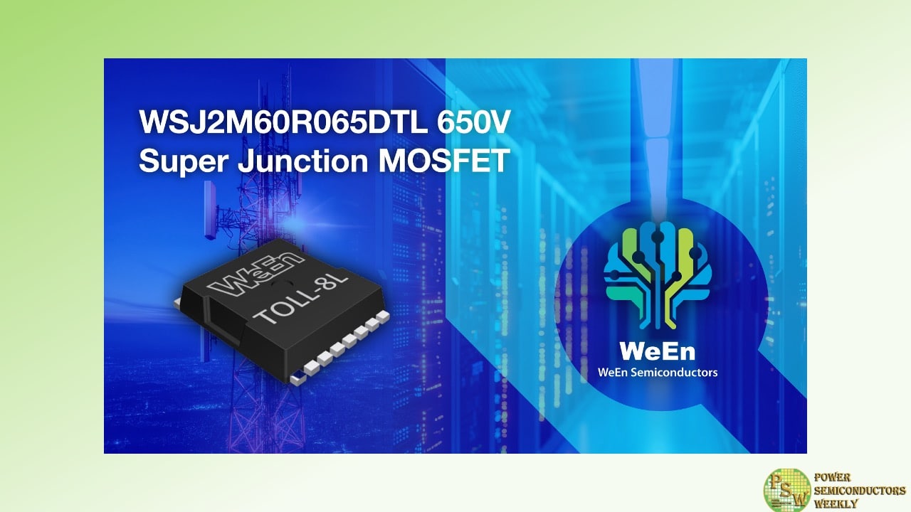
WeEn Semiconductors will exhibit the company’s latest 600 V super junction MOSFET for computing and telecoms server applications at this year’s PCIM Expo conference and trade fair. The WSJ2M60R065DTL has been specifically developed to address the demands of artificial intelligence (AI) and other high-performance processing applications by enabling improved efficiency, smaller form factors and easier thermal management.
Based on the company’s latest generation super junction technology, the WeEn WSJ2M60R065DTL super junction MOSFET combines an industry-leading on resistance (RDS(ON)) and figure of merit (RDS(ON)*Qg) with an ultra-compact TOLL package. Visitors to PCIM in Nuremberg from 6th – 8th May 2025 will have the opportunity to see this advanced technology on the WeEn booth (Hall 9, booth 131), alongside other bipolar products including silicon-controlled rectifiers, power diodes, high voltage transistors and silicon carbide (SiC) devices.
The WSJ2M60R065DTL is rated for 50 A, features a maximum RDS(ON) of 65 mΩ and has a typical blocking voltage of around 700 V. An integrated and fine-tuned forward recovery diode (FRD) ensures excellent reverse recovery robustness and balanced high-temperature performance. The body diode can withstand a commutation speed of 1000 A/μs without damage, making the WSJ2M60R065DTL particularly suitable for Zero Voltage Switching (ZVS) applications in soft-switching topologies where it can deliver high efficiency while handling irregular operating conditions. At the same time, stable resistance performance delivers a steady and predictable RDS(ON) across a range of current and temperature conditions.
In developing the new MOSFET, WeEn has focused on precise control of the charge balance of the super junction structure. This ensures robust avalanche ruggedness and low capacitive losses that allow for an optimized balance of RDS(ON) and EOSS As with all WeEn technologies, reliability is a prime consideration and the company conducts extensive and reliability checks. All of the company’s super junction MOSFETs demonstrate not only consistency among samples but good ESD capabilities and zero aging during reliability examinations.
Original – WeEn Semiconductors
-

The market for electric vehicles continues to gather pace with a strong volume growth of both battery electric vehicles (BEVs) and plug-in hybrid electric vehicles (PHEVs). The share of electric vehicles produced is expected to see double-digit growth by 2030 with a share of around 45 percent compared to 20 percent in 2024. Infineon Technologies AG is responding to the growing demand for high-voltage automotive IGBT chips by launching a new generation of products. Among these offerings are the EDT3 (Electric Drive Train, 3 rd generation) chips, designed for 400 V and 800 V systems, and the RC-IGBT chips, tailored specifically for 800 V systems. These devices enhance the performance of electric drivetrain systems, making them particularly suitable for automotive applications.
The EDT3 and RC-IGBT bare dies have been engineered to deliver high-quality and reliable performance, empowering customers to create custom power modules. The new generation EDT3 represents a significant advancement over the EDT2, achieving up to 20 percent lower total losses at high loads while maintaining efficiency at low loads. This achievement is due to optimizations that minimize chip losses and increase the maximum junction temperature, balancing high-load performance and low-load efficiency. As a result, electric vehicles using EDT3 chips achieve an extended range and reduce energy consumption, providing a more sustainable and cost-effective driving experience.
“Infineon, as a leading provider of IGBT technology, is committed to delivering outstanding performance and reliability”, says Robert Hermann, Vice President for Automotive High Voltage Chips and Discretes at Infineon Technologies. “Leveraging our steadfast dedication to innovation and decarbonization, our EDT3 solution enables our customers to attain ideal results in their applications.”
The EDT3 chipsets, which are available in 750 V and 1200 V classes, deliver high output current, making them well-suited for main inverter applications in a diverse range of electric vehicles, including battery electric vehicles, plug-in hybrid electric vehicles, and range-extended electric vehicles (REEVs). Their reduced chip size and optimized design facilitate the creation of smaller modules, consequently leading to lower overall system costs. Moreover, with a maximum virtual junction temperature of 185°C and a maximum collector-emitter voltage rating of up to 750 V and 1200 V, these devices are well-suited for high-performance applications, enabling automakers to design more efficient and reliable powertrains that can help extend driving range and reduce emissions.
“Infineon, as Leadrive’s primary IGBT chip supplier and partner, consistently provides us with innovative solutions that deliver system-level benefits,” said Dr. Ing. Jie Shen, Founder and General Manager of Leadrive. “The latest EDT3 chips have optimized losses and loss distribution, support higher operating temperatures, and offer multiple metallization options. These features not only reduce the silicon area per ampere, but also accelerate the adoption of advanced packaging technologies.”
The 1200 V RC-IGBT elevates performance by integrating IGBT and diode functions on a single die, delivering an even higher current density compared to separate IGBT and diode chipset solutions. This advancement translates into a system cost benefit, attributed to the increased current density, scalable chip size, and reduced assembly effort.
Infineon’s latest EDT3 IGBT chip technology is now integrated into the HybridPACK™ Drive G2 automotive power module, delivering enhanced performance and capabilities across the module portfolio. This module offers a power range of up to 250 kW within the 750 V and 1200 V classes, enhanced ease of use, and new features such as an integration option for next-generation phase current sensors and on-chip temperature sensing, contributing to system cost improvements.
All chip devices are offered with customized chip layouts, including on-chip temperature and current sensors. Additionally, metallization options for sintering, soldering and bonding are available on request.
The new EDT3 and RC-IGBT devices are already available for sampling. Further information is available at www.infineon.com/edt3
Original – Infineon Technologies
-

ROHM has developed N-channel power MOSFETs featuring industry-leading low ON-resistance and wide SOA capability. They are designed for power supplies inside high-performance enterprise and AI servers.
The advancement of high-level data processing technologies and the acceleration of digital transformation have increased the demand for data center servers. At the same time, the number of servers equipped with advanced computing capabilities for AI processing is on the rise and is expected to continue to grow. These servers operate 24 hours a day, 7 days a week – ensuring continuous operation. As a result, conduction losses caused by the ON-resistance of multiple MOSFETs in the power block have a significant impact on system performance and energy efficiency. This becomes particularly evident in AC-DC conversion circuits, where conduction losses make up a substantial portion of total power loss – driving the need for low ON-resistance MOSFETs.
Additionally, servers equipped with a standard hot-swap function, which allow for the replacement and maintenance of internal boards and storage devices while powered ON, experience a high inrush current during component exchanges. Therefore, to protect server components and MOSFETs from damage, a wide Safe Operating Area (SOA) tolerance is essential.
To address these challenges, ROHM has developed its new DFN5060-8S package that supports the packaging of a larger die compared to conventional designs, resulting in a lineup of power MOSFETs that achieve industry-leading low ON-resistance along with wide SOA capability. These new products significantly contribute to improving efficiency and enhancing reliability in server power circuits.
The new lineup includes three products. The RS7E200BG (30V) is optimized for both secondary-side AC-DC conversion circuits and hot-swap controller (HSC) circuits in 12V power supplies used in high-performance enterprise servers. The RS7N200BH (80V) and RS7N160BH (80V) are ideal for secondary AC-DC conversion circuits in 48V AI server power supplies.
All three models feature the newly developed DFN5060-8S package (5.0mm × 6.0mm). The package increases the internal die size area by approximately 65% compared to the conventional HSOP8 package (5.0mm × 6.0mm). As a result, the RS7E200BG (30V) and RS7N200BH (80V) achieve ON-resistances of 0.53mΩ and 1.7mΩ (at VGS = 10V), respectively – both of which rank among the best in the industry in the 5.0mm × 6.0mm class, significantly contributing to higher efficiency in server power circuits.
Moreover, ROHM has optimized the internal clip design to enhance heat dissipation, further improving SOA tolerance, which contributes to ensuring application reliability. Notably, the RS7E200BG (30V) achieves an SOA tolerance of over 70A at a pulse width of 1ms and VDS = 12V, which is twice that of the conventional HSOP8 package MOSFETs under the same conditions, ensuring industry-leading SOA performance in a 5.0mm × 6.0mm footprint.
Going forward, ROHM plans to gradually begin mass production of power MOSFETs compatible with hot-swap controller circuits for AI servers in 2025, continuing to expand its lineup that contributes to greater efficiency and reliability across a wide range of applications.
Original – ROHM
-

Mitsubishi Electric Corporation will begin shipping samples of its new XB Series high-voltage insulated-gate bipolar transistor (HVIGBT) module, a 3.3k-volt, 1500A high-capacity power semiconductor for large industrial equipment such as railway vehicles, on May 1.
By adopting proprietary diode and insulated gate bipolar transistor (IGBT) elements, as well as a unique chip termination structure, the module’s improved moisture resistance will help to improve the efficiency and reliability of inverters for large industrial equipment operating in diverse environments. Mitsubishi Electric will exhibit the XB Series HVIGBT module at Power Conversion Intelligent Motion (PCIM) Expo & Conference 2025 in Nuremberg, Germany from May 6 to 8.
The new 3.3kV/1500A XB Series HVIGBT module uses IGBT elements incorporating Mitsubishi Electric’s proprietary relaxed field of cathode (RFC) diode and carrier-stored trench-gate bipolar transistor (CSTBT) structure. In particular, the module reduces total switching loss by approximately 15% compared to previous models, contributing to higher efficiency in inverters. It also expands tolerance in the reverse-recovery safe-operating area (RRSOA) by about 25% compared to previous models, further enhancing inverter reliability.
In addition, by using a new electric field relaxation structure and a surface charge control structure in the chip’s termination area, Mitsubishi Electric has reduced the area’s size by about 30% while achieving about 20 times greater moisture resistance than existing products, contributing to more stable operation of inverters used in high-humidity environments. By further improving the efficiency and reliability of inverters for large industrial equipment operating in various environments, the module is expected to contribute to efforts to achieve carbon neutrality.
Original – Mitsubishi Electric
-

Infineon Technologies AG is developing TRENCHSTOP™ 7 H7 IGBTs in the new DTO247 package, which has the size of two TO247 packages. With a nominal current rating of up to 350 A, they will be the most powerful discrete IGBTs on the market. The new devices are ideal for solar inverters, uninterruptible power supplies (UPS) and energy storage systems (ESS).
The DTO247 with a single high-current IGBT can replace multiple lower-current IGBTs in standard TO247 packages that are typically connected in parallel. This enables high power density and bridges the gap between TO247-based designs and module architectures. Moreover, the ability to mix and match DTO247-based and standard TO247-based architectures within the same system offers a high degree of flexibility and customization. Integrating DTO247 into the existing TO247 portfolio simplifies the development of cost-effective, scalable architectures.
This reduces design complexity, shortens development time and lowers parallelization effort while improving performance, reliability, and system cost-effectiveness. The portfolio will include H7 IGBTs in 1200 V and 750 V versions, with current ratings of 200 A, 250 A, 300 A, and 350 A. Designed for high-current applications, these devices feature 2-mm-wide leads for optimal conduction, along with 7 mm pin-to-pin clearance and 10 mm creepage distance for enhanced safety and reliability. Additionally, an integrated Kelvin emitter pin provides faster and more efficient switching performance.
Infineon intends to continuously expand its DTO247 portfolio, with plans to include CoolSiC™ MOSFETs in a half-bridge configuration. These devices target to be pin-to-pin compatible with similar products on the market.
First engineering samples of the 200 A and 350 A variants of the TRENCHSTOP™ 7 H7 IGBTs in the DTO247 package are available now. Volume production is scheduled for mid-2026.
Original – Infineon Technologies
-

Vishay Intertechnology, Inc. introduced a new Gen 4.5 650 V E Series power MOSFET that delivers high efficiency and power density for telecom, industrial, and computing applications. Compared to previous-generation devices, the Vishay Siliconix n-channel SiHK050N65E slashes on-resistance by 48.2 %, while offering a 65.4 % lower resistance times gate charge, a key figure of merit (FOM) for 650 V MOSFETs used in power conversion applications.
Vishay offers a broad line of MOSFET technologies that support all stages of the power conversion process, from high voltage inputs to the low voltage outputs required to power the latest high tech equipment. With the SiHK050N65E and other devices in the Gen 4.5 650 V E Series family, the company is addressing the need for efficiency and power density improvements in two of the first stages of the power system architecture — power factor correction (PFC) and subsequent DC/DC converter blocks.
Typical applications will include servers, edge computing, and super computers; UPS; high intensity discharge (HID) lamps and fluorescent ballast lighting; telecom SMPS; solar inverters; welding equipment; induction heating; motor drives; and battery chargers.
Built on Vishay’s latest energy-efficient E Series superjunction technology, the SiHK050N65E’s low typical on-resistance of 0.048 Ω at 10 V results in a higher power rating for applications > 6 kW. With 50 V of additional breakdown voltage, the 650 V device addresses 200 VAC to 277 VAC input voltages and the Open Compute Project’s Open Rack V3 (ORV3) standards. In addition, the MOSFET offers ultra low gate charge down to 78 nC. The resulting FOM of 3.74 Ω*nC translates into reduced conduction and switching losses to save energy and increase efficiency. This allows the device to address the specific titanium efficiency requirements in server power supplies or reach 96 % peak efficiency.
For improved switching performance in hard-switched topologies such as PFC and two-switch forward designs, the MOSFET released today provides low typical effective output capacitances Co(er) and Co(tr) of 167 pF and 1119 pF, respectively. The device’s resulting resistance times Co(er) FOM is an industry-low 8.0 Ω*pF. The SiHK050N65E is offered in the PowerPAK® 10 x 12 package with a Kelvin connection for reduced gate noise and provides increased dv/dt ruggedness. RoHS-compliant and halogen-free, the MOSFET is designed to withstand overvoltage transients in avalanche mode with guaranteed limits through 100 % UIS testing.
Original – Vishay Intertechnology
-

The 600 V CoolMOS™ 8 high-voltage superjunction (SJ) MOSFET product family from Infineon Technologies AG has allowed Enphase Energy, a global energy technology company and a leading supplier of microinverter-based solar and battery systems, to simplify its system design and reduce assembly costs. By using the 600 V CoolMOS 8 SJ, Enphase is able to significantly reduce MOSFET resistance (R DS(on)) for its solar inverter systems, leading to lower conduction losses, which improves overall device efficiency and boosts power density. In addition, the company achieved MOSFET related cost savings.
“We are thrilled to partner with Enphase and support their mission to deliver innovative solar energy solutions,” said Richard Kuncic, Senior Vice President and General Manager at Infineon. “Our 600 V CoolMOS 8 SJ MOSFETs are designed to provide superior efficiency, reliability, and cost savings, which aligns perfectly with Enphase’s and Infineon’s commitment to advancing the performance and affordability of renewable energy technologies, further driving decarbonization.”
“Collaborating with Infineon has allowed us to leverage their CoolMOS 8 SJ MOSFET technology to enhance the performance and cost-effectiveness of our microinverter systems,” said Aaron Gordon, Senior Vice President and General Manager of the Systems Business Unit at Enphase Energy. “This partnership underscores our dedication to innovation and excellence in the solar energy industry, and we are excited about the significant improvements in power density and cost savings that we are now able to offer our customers.”
Infineon’s latest CoolMOS 8 MOFETs at 600 V are leading the way in high-voltage superjunction MOSFET technology worldwide, setting the standard for both technology and price performance on a global scale. The technology increases overall system performance and further reinforces decarbonization in applications such as chargers and adapters, solar and energy storage systems, EV charging, and uninterruptible power supplies (UPS).
The CoolMOS 8 SJ MOSFETs have an 18 percent lower gate charge than the CFD7 and 33 percent lower than the P7 series. A reduced gate charge allows for less electric charge to be applied to the gate of a MOSFET to switch it from the off state (non-conducting) to the on state (conducting), enabling a more energy-efficient system performance.
Additionally, the CoolMOS 8 SJ MOSFETs have the quickest turn-off time in the market and their thermal performance has been improved by 14 to 42 percent compared to the previous generation. The 600 V CoolMOS 8 SJ technology is equipped with an integrated fast body diode and is available in SMD-QDPAK, TOLL, and Thin-TOLL 8×8 packages, making it suitable for a wide range of consumer and industrial applications.
Samples for the portfolio extension of 600 V CoolMOS 8 SJ MOSFETs and 650 V CoolMOS 8 SJ MOSFETs are available from early April on.
Original – Infineon Technologies
