-
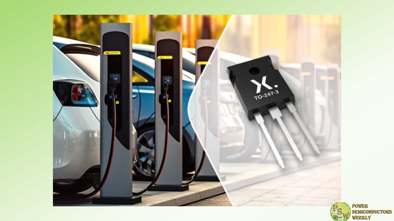
Nexperia announced its first silicon carbide (SiC) MOSFETs with the release of two 1200 V discrete devices in 3-pin TO-247 packaging with RDS(on) values of 40 mΩ and 80 mΩ. NSF040120L3A0 and NSF080120L3A0 are the first in a series of planned releases which will see Nexperia’s SiC MOSFET portfolio quickly expand to include devices with a variety of RDS(on) values in a choice of through-hole and surface mounted packages.
This release addresses the market demand for the increased availability of high performance SiC MOSFETs in industrial applications including electric vehicle (EV) charging piles, uninterruptible power supplies (UPS) and inverters for solar and energy storage systems (ESS).
“With these inaugural products, Nexperia and Mitsubishi Electric wanted to bring true innovation to a market that has been crying out for more wide-bandgap device suppliers”, according to Katrin Feurle, Senior Director & Head of Product Group SiC at Nexperia. “Nexperia can now offer SiC MOSFET devices which offer best-in-class performance across several parameters, including high RDS(on) temperature stability, low body diode voltage drop, tight threshold voltage specification as well as a very well-balanced gate charge ratio making the device safe against parasitic turn on. This is the opening chapter in our commitment to producing the highest quality SiC MOSFETs in our partnership with Mitsubishi Electric. Together we will undoubtedly push the boundaries of SiC device performance over the coming years”.
“Together with Nexperia, we’re thrilled to introduce these new SiC MOSFETs as the first product of our partnership”, says Toru Iwagami, Senior General Manger, Power Device Works, Semiconductor & Device Group in Mitsubishi Electric. “Mitsubishi Electric has accumulated superior expertise of SiC power semiconductors, and our devices deliver a unique balance of characteristics.”RDS(on) is a critical performance parameter for SiC MOSFETs as it impacts conduction power losses. Nexperia identified this as a limiting factor in the performance of many currently available SiC devices and used its innovative process technology to ensure its new SiC MOSFETs offer industry-leading temperature stability, with the nominal value of RDS(on) increasing by only 38% over an operating temperature range from 25°C to 175°C. Unlike other many currently available SiC devices in the market.
Nexperia’s SiC MOSFETs also exhibit the very low total gate charge (QG), which brings the advantage of lower gate drive losses. Furthermore, Nexperia balanced gate charge to have an exceptionally low ratio of QGD to QGS, a characteristic which increases device immunity against parasitic turn-on.
Together with the positive temperature coefficient of SiC MOSFETs, Nexperia’s SiC MOSFETs offers also ultra-low spread in device-to device threshold voltage, VGS(th), which allows very well-balanced current-carrying performance under static and dynamic conditions when devices are operated in parallel. Furthermore, low body diode forward voltage (VSD) is a parameter which increases device robustness and efficiency, while also relaxing the dead-time requirement for asynchronous rectification and free wheel operation.
Nexperia is also planning the future release of automotive grade MOSFETs. The NSF040120L3A0 and NSF080120L3A0 are available in production quantities now. Please contact Nexperia sales representatives for samples of the full SiC MOSFET offering.
Original – Nexperia
-
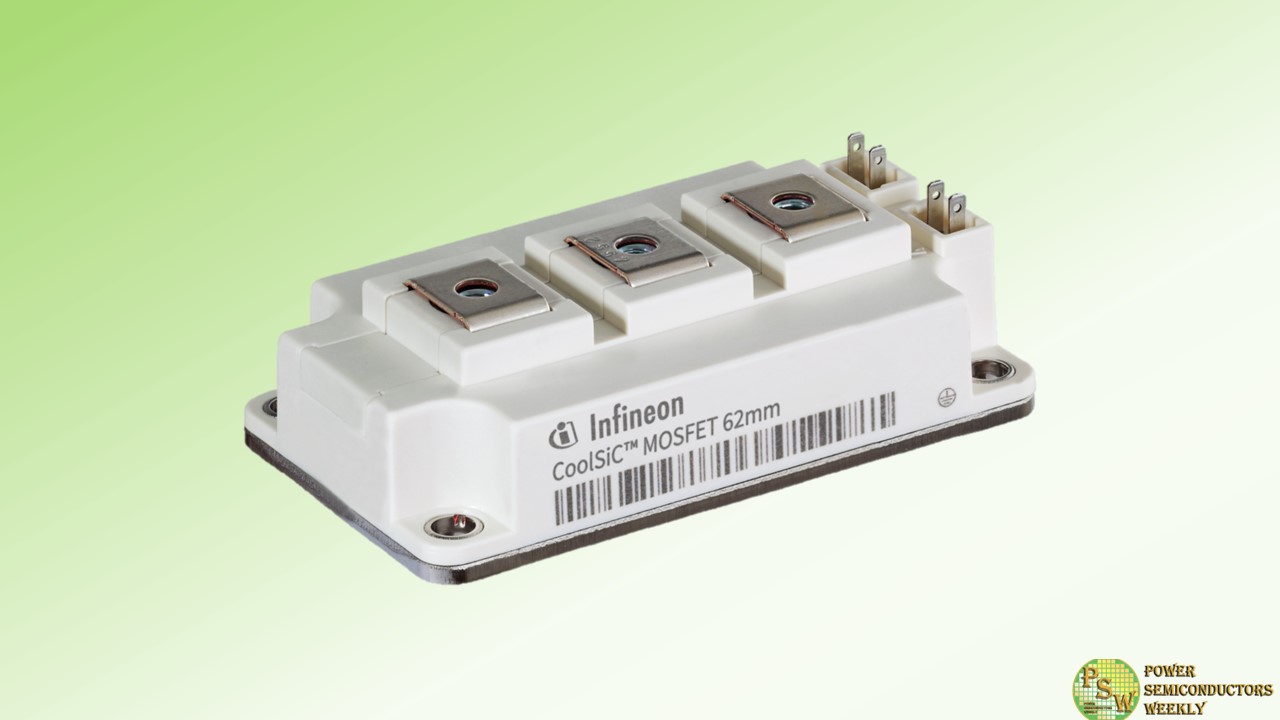
Infineon Technologies AG announced the expansion of its CoolSiC 1200 V and 2000 V MOSFET module families with a new industry-standard package. The proven 62mm device is designed in half-bridge topology and is based on the recently introduced and advanced M1H silicon carbide (SiC) MOSFET technology.
The package enables the use of SiC for mid-power applications from 250 kW – where silicon reaches the limits of power density with IGBT technology. Compared to a 62mm IGBT module, the list of applications now additionally includes solar, server, energy storage, EV charger, traction, commercial induction cooking and power conversion systems.
The M1H technology enables a significantly wider gate voltage window, ensuring high robustness to driver and layout-induced voltage spikes at the gate without any restrictions even at high switching frequencies. In addition to that, very low switching and transmission losses minimize cooling requirements.
Combined with a high reverse voltage, these devices meet another requirement of modern system design. By using Infineon’s CoolSiC chip technology, converter designs can be made more efficient, the nominal power per inverter can be increased and system costs can be reduced.
With baseplate and screw connections, the package features a very rugged mechanical design optimized for highest system availability, minimum service costs and downtime losses. Outstanding reliability is achieved through high thermal cycling capability and a continuous operating temperature (T vjop) of 150°C. The symmetrical internal package design provides identical switching conditions for the upper and lower switches. Optionally, the thermal performance of the module can be further enhanced with pre-applied thermal interface material (TIM).
The CoolSiC 62mm package MOSFETs are available in 1200 V variants of 5 mΩ/180 A, 2 mΩ/420 A and 1 mΩ/560 A. The 2000 V portfolio will include the 4 mΩ/300 A and 3 mΩ/400 A variants. The portfolio will be completed in Q1 2024 with the 1200 V/3 mΩ and 2000 V/5 mΩ variants.
An evaluation board is available for rapid characterization of the modules (double pulse/continuous operation). For ease of use, it provides flexible adjustment of the gate voltage and gate resistors. At the same time, it can be used as a reference design for driver boards for volume production.
Original – Infineon Technologies
-
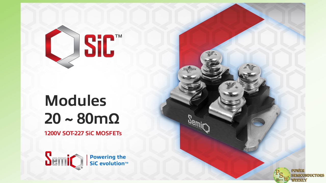
SemiQ announced that it has expanded its portfolio of QSiC™ Silicon Carbide modules with the launch of a family of 1200V MOSFETs that pairs with or without 1200V SiC Schottky Diodes in a SOT-227 package.
Crafted from high-performance ceramics and rigorously engineered to function with unwavering reliability in challenging conditions, the newly introduced SemiQ SiC modules achieve remarkably high performance. This enhanced performance empowers higher power densities and more streamlined design configurations.
The QSiC™ modules feature high breakdown voltage (> 1400 V), high-temperature operation (Tj = 175 °C), and low Rds(On) shift over the full operating temperature range while providing industry-leading gate oxide stability and gate oxide lifetime, avalanche (UIS) ruggedness, and extended short-circuit withstand times.
Target markets for the new QSiC™ modules with our existing SOT-227 SiC SBD modules include EV charging, on-board chargers (OBCs), DC-DC converters, E-compressors, fuel cell converters, medical power supplies, energy storage systems, solar and wind energy systems, data center power supplies, UPS/PFC circuits, and other automotive and industrial power applications.
All of the new QSiC™ modules are tested at wafer-level gate burn-in to provide high-quality gate oxide with stable gate threshold voltage. Besides the burn-in test, which helps to stabilize the extrinsic failure rate, stress tests such as gate stress, high-temperature reverse bias (HTRB) drain stress, and high humidity, high voltage, high temperature (H3TRB) to ensure requisite industrial grade quality levels.
Dr. Timothy Han, President at SemiQ, said, “We are delighted with the customer input and needs for our new family of QSiC™ high-power modules and thank our SemiQ team who have worked tirelessly to build and qualify our latest QSiC™ modules.”
SemiQ’s new 1200V SOT-227 modules are available in 20mΩ, 40mΩ, 80mΩ SiC MOSFET categories. A table with part numbers is shown below.
Part Numbers Circuit Configuration Ratings, Packages Rds(on), mΩ GCMX020B120S1-E1 Single MOSFET w/o SBD 1200V/113A, SOT-227 20 GCMS020B120S1-E1 Single MOSFET w SBD 1200V/113A, SOT-227 20 GCMX040B120S1-E1 Single MOSFET w/o SBD 1200V/57A, SOT-227 40 GCMS040B120S1-E1 Single MOSFET w SBD 1200V/57A, SOT-227 40 GCMX080B120S1-E1 Single MOSFET w/o SBD 1200V/30A, SOT-227 80 GCMS080B120S1-E1 Single MOSFET w SBD 1200V/30A, SOT-227 80 Original – SemiQ
-
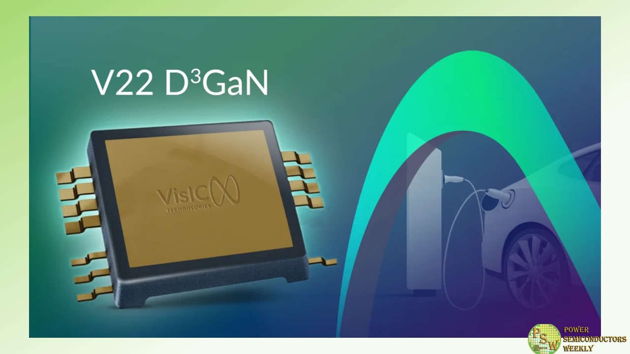
VisIC Technologies announced that the samples of the V22TG D3GAN will be available in the first quarter of 2024. This early availability allows manufacturers to assess and experience the performance and benefits of the package firsthand, aiding in the rapid development of the next generation of systems.
Key Features and Benefits:
1. Advanced Leaded Top-Side Cooled Isolated.
2. Automotive and High Voltage Capability.
3. High Power Density and Low On-Resistance.
4. Versatile and Easy to Implement.Dr. Tamara Baksht, CEO and Co-Founder: “This advanced power package not only offers exceptional performance and reliability but also provides the versatility and ease of implementation required for emerging automotive and industrial applications. We are confident that the V22TG D3GAN will empower manufacturers to accelerate the adoption of electric vehicles.”
Original – VisIC Technologies
-

The Hanau-based technology company Heraeus has acquired a significant stake in the start-up company Zadient. Heraeus, as a German high-tech materials player considers the market of SiC base material highly relevant and a suitable addition to its other operations.
The French-German firm Zadient specializes in the production of silicon carbide source material. Silicon carbide is a wide band gap semiconductor material, which is currently gaining rapid traction in the semiconductor market. Its properties lend themselves to use in power semiconductors, which help to convert current and voltages.
Its fundamental contribution is the dramatic increase in efficiency it provides over silicon by reducing the heat losses that occur while power passes through chips. Its ability to handle higher power densities with low losses allows for the transition from 400V to 800V battery systems in EVs which significantly shortens their charging time and increases their range. SiC based electronics are also smaller and lighter, which also contributes to increased range.
These properties have lead to the rapid adoption of SiC in applications ranging from the main inverters and on-board chargers in EVs to wind and solar power inverters, battery storage systems and even airplane power management modules. The breadth of these few examples is already an indication of the significant role SiC will play in the mobility and energy transition.
Through the partnership, Heraeus intends to accelerate the company’s growth and support Zadient’s innovative approach with its own know-how.
“Heraeus recognizes the potential of the SiC market and considers it to be highly relevant for high-tech applications. By acquiring a stake in Zadient, we can jointly offer our customers even better solutions” said Steffen Metzger, member of the Heraeus Group Management Committee. “We are very happy that we found a way to accelerate growth in the SiC market by combining the innovative ideas of the materials start-up Zadient with the manufacturing and technical expertise of the Heraeus Group.”
“We are very excited to be partnering with an industry leader like Heraeus,” noted Zadient CEO Kagan Ceran. “The expertise that Heraeus has in the industrial scale production of advanced materials, both in its home market of Germany and abroad, offers us unique synergies as we strive to realize our vision to be the world’s largest volume, highest purity producer of silicon carbide semiconductor materials.”
Original – Heraeus
-
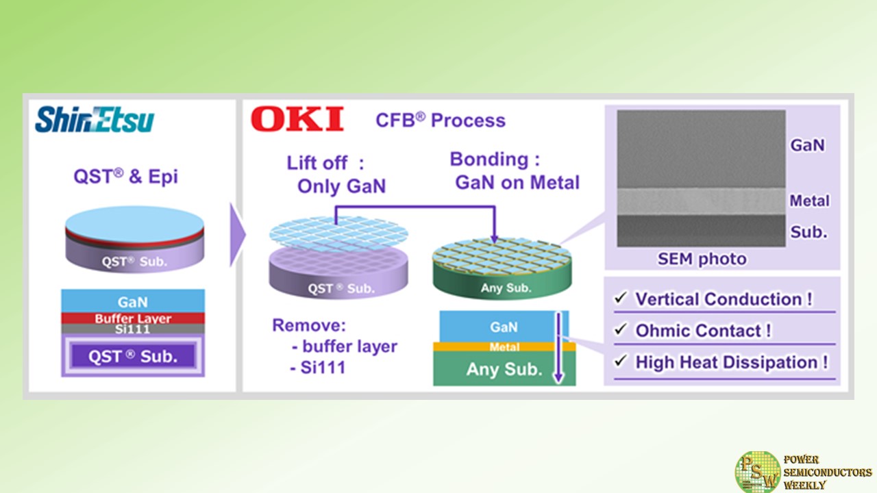
OKI, in collaboration with Shin-Etsu Chemical Co., Ltd., has announced the successful development of a technology that uses OKI’s CFB (crystal film bonding) technology to lift off only the GaN (gallium nitride) functional layer from Shin-Etsu Chemical’s uniquely improved QST® (Qromis Substrate Technology) substrate and bond it to a different material substrate.
This technology enables the vertical conduction of GaN and is expected to contribute to the realization and commercialization of vertical GaN power devices capable of controlling large currents. The two companies will work further together to develop vertical GaN power devices that can be implemented in society by partnering with companies that manufacture these devices.
GaN devices are attracting attention as next-generation devices that combine high device characteristics with low power consumption, such as power devices that require high breakdown voltages of 1800 volts or more, high-frequency devices for Beyond5G, and high-brightness micro-LED displays.
In particular, vertical GaN power devices are expected to achieve significant demand growth as devices that can improve the basic performance of electric vehicles by endowing them with extended driving ranges and shortened power supply times. However, two major challenges hinder the social implementation of vertical GaN power devices: the diameter of the wafers must be increased to improve productivity and vertical conductivity must be realized to enable large current control.
The coefficient of thermal expansion of Shin-Etsu Chemical’s QST substrate is equivalent to that of GaN. It can suppress warpage and cracking. This characteristic enables the crystal growth of thick GaN films with high breakdown voltages even on wafers larger than 8 inches, thereby enabling the production of wafers with larger diameters.
On the other hand, OKI’s CFB technology can lift off only the GaN functional layer from the QST substrate while maintaining high device characteristics. The insulating buffer layer required for GaN crystal growth can be removed and bonded to various substrates via metal electrodes that allow ohmic contact.
Bonding of these functional layers to a conductive substrate with high heat dissipation will enable both high heat dissipation and vertical conductivity. Through this, the combined technologies of Shin-Etsu Chemical and OKI solve the above two major challenges, paving the way for the social implementation of vertical GaN power devices.
In the future, the two companies will contribute to the realization and widespread use of vertical GaN power devices through Shin-Etsu Chemical’s provision of QST substrates or GaN grown QST substrates to companies manufacturing GaN devices and OKI’s provision of CFB technology through partnering and licensing.
Furthermore, OKI hopes to use CFB technology to provide added value to semiconductor devices that go beyond the framework of single materials and help realize the company’s key message of “Delivering OK! to your life”.
Original – OKI
-
Mitsubishi Electric Corporation announced that it will enter into a strategic partnership with Nexperia B.V. to jointly develop silicon carbide (SiC) power semiconductors for the power electronics market. Mitsubishi Electric will leverage its wide-bandgap semiconductor technologies to develop and supply SiC MOSFET chips that Nexperia will use to develop SiC discrete devices.
The electric vehicle market is expanding worldwide and is helping to drive the exponential growth of SiC power semiconductors, which offer lower energy loss, higher operating temperatures and faster switching speeds than conventional silicon power semiconductors. The high efficiency of SiC power semiconductors is expected to contribute significantly to global decarbonization and green transformation.
Mitsubishi Electric has established leading positions in applications such as high-speed trains, high-voltage industrial applications and home appliances. The company launched the world’s first SiC power modules for air conditioners in 2010 and became the first supplier of an all-SiC power module for Shinkansen bullet trains in 2015. Mitsubishi Electric has accumulated superior expertise for the development and manufacture of SiC power modules, which are known for their advanced performance and high reliability.
Going forward, Mitsubishi Electric expects to strengthen its partnership with Nexperia, a global leader with decades of experience in the design, manufacture, quality assurance and supply of diverse discrete devices. Nexperia’s devices are used in the automotive, industrial, mobile and consumer markets, contributing to decarbonization and a more sustainable future. Mitsubishi Electric will continue to improve the performance and quality of its SiC chips and focus on the development of power modules using proprietary module technologies.
Mark Roeloffzen, SVP & General Manager Business Group Bipolar Discretes at Nexperia, said: “This mutually beneficial strategic partnership with Mitsubishi Electric represents a significant stride in Nexperia’s silicon carbide journey. Mitsubishi Electric has a strong track record as a supplier of technically proven SiC device and modules. Combined with Nexperia’s high-quality standards and expertise in discrete products and packaging, we will certainly generate positive synergies between both companies – ultimately enabling our customers to deliver highly energy efficient products in the industrial, automotive or consumer markets they serve.”
Masayoshi Takemi, Executive Officer and Group President, Semiconductor & Device at Mitsubishi Electric, said: “Nexperia is a leading company in the industrial sector with proven technologies for high quality discrete semiconductors. We are delighted to enter into this co-development partnership that will leverage the semiconductor technologies of both companies.”
Original – Mitsubishi Electric
-
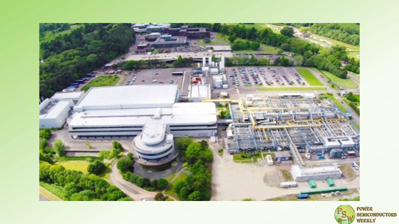
Vishay Intertechnology, Inc. and Nexperia B.V. announced that they have entered into an agreement that Vishay will acquire Nexperia’s wafer fabrication facility and operations located in Newport, South Wales, U.K. for $177million in cash. ATREG, Inc., the Seattle-based premier global firm for initiating, brokering, and executing the exchange of semiconductor manufacturing assets, served as Nexperia’s transaction advisors.
Newport wafer fab, located on 28 acres, is an automotive certified, 200mm semiconductor wafer fab that supplies primarily automotive markets. It is the largest semiconductor manufacturer in the U.K.
Toni Versluijs, Country Manager Nexperia UK, stated: “Nexperia would have preferred to continue the long-term strategy it implemented when it acquired the investment-starved fab in 2021 and provided for massive investments in equipment and personnel. However, these investment plans have been cut short by the unexpected and wrongful divestment order made by the UK Government in November 2022.The site needs clarity about its future to avoid further losses, and today’s announcement provides this. Of all options, this agreement with Vishay is the most viable one to secure the future of the site as Vishay – like Nexperia – has a solid customer base for the fab’s capabilities. For the site, Vishay’s commitment to further make the Newport wafer fab a success story is encouraging. Nexperia’s position with regards to the UK Government’s order remains unchanged.”
The closing of Newport wafer fab transaction is subject to UK government review, the purchase rights of a third party, and customary closing conditions, and is expected to occur in the first quarter of 2024.
Nexperia’s priority always remains with our employees and our customers. Whilst we work on ensuring that all conditions to the sale are met soonest, we will continue to own and manage the site and support the employees as usual.
Original – Nexperia
-
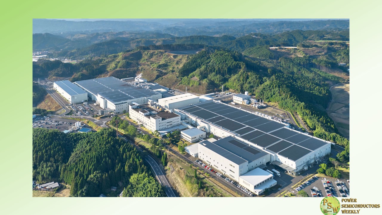
ROHM has completed the acquisition of the assets of Solar Frontier’s former Kunitomi Plant located in Japan, on November 7, 2023, based on its basic agreement signed with Solar Frontier.
The Plant will be operated by LAPIS Semiconductor, a subsidiary of the ROHM Group, as its Miyazaki Plant No.2. It will become the Group’s main production site for SiC power devices and is aiming to start operation during 2024.
The ROHM Group will continue to strengthen its production capacity in accordance with its Medium-Term Management Plan while keeping abreast of market conditions, and will also thoroughly enhance its BCM system to ensure a stable supply of products to customers.
Original – ROHM
-
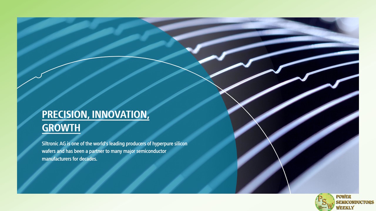
Siltronic announced the production of the first wafers in its latest state-of-the-art 300 mm fab in Singapore. The production marks an important milestone in the strategic capacity expansion of Siltronic’s global production network.
“It fills me with immense pride to see the production of the first wafers from the line. This is a decisive milestone in the history of Siltronic. I am delighted to see that the test wafer production has started slightly ahead of schedule. I would therefore like to congratulate and thank all the employees and suppliers involved for their contributions. We look forward to supplying our customers with leading-edge wafers from this new state-of-the-art fab,” said Dr. Michael Heckmeier, CEO of Siltronic AG.
Despite many challenges, including the global pandemic and supply chain constraints, the construction of the new fab, which started in 2021, is on schedule and on budget. By the end of 2024, around 2 billion Euro will have been invested into this greenfield project. This will be followed by further investments on a smaller scale to further ramp the production.
The large-scale project covers an area of approximately 20 soccer fields. At peak construction times, more than 5,000 workers were on site for both construction activities and facilities installation. The fab is supported by approximately 5,500 piles which extend up to 60 meters into the ground. In total, 150,000 m³ of concrete and more than 35,000 tons of steel have been used.
In the mid-term, the new fab is expected to be highly cost efficient due to the high degree of automation and deployment of digitalization, coupled with its strategic proximity to the existing 200- and 300 mm fabs in Singapore, which will lead to economies of scale and synergies.
The new fab will serve both medium and long-term demand growth in the semiconductor market, which is driven by megatrends such as digitalization, artificial intelligence, and electromobility. As originally planned, the production ramp phase will commence from the beginning of next year.
“The trust and support of our customers has been a key factor for this investment. In the ramp phase, sales from the new fab have been secured to a high degree by long-term agreements. Customers have also contributed significantly to the initial financing of the fab through prepayments,” added Claudia Schmitt, CFO of Siltronic AG.
Original – Siltronic
