-
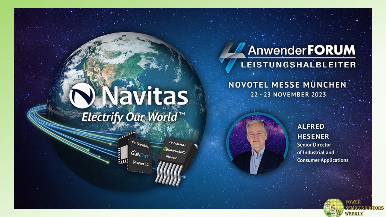
Navitas Semiconductor announced its participation in the Power Semiconductor User Forum, organized by WEKA Fachmedien on November 22nd -23rd, 2023. The event offers valuable insights into power electronics for developers and technical buyers.
Alfred Hesener, Senior Director of Industrial and Consumer Applications will explore “Reliability and Cost-of-Ownership Optimization in Industrial Power Supplies,” on November 23rd at 1:45 p.m. CET. Mr. Hesener will highlight next-generation solutions that achieve high power densities, cool operation, robust performance using Navitas’ GaNSense single and Half-Bridge power ICs.
Navitas’ GaNFast power ICs integrate GaN power and drive with control, sensing, and protection to enable faster charging, higher power density, greater energy savings and system cost reduction. In addition, each GaN power IC saves over 4 kg CO2 due to higher efficiency and dematerialization. New ‘Gen-3 Fast’ GeneSiC MOSFETs have up to 50% improved performance vs. other SiC devices, and save over 40 kg CO2 per unit vs. legacy silicon IGBTs.
“For industrial power designers, the WEKA forum highlights leading-edge, reliable technology for drives, pumps, chargers and power conversion, using GaN and SiC,” said Mr. Hesener. “Features like loss-less current sensing, programmable dV/dt, 2 kV ESD protection and autonomous sensing and protection are key enablers, and reduce time to market.”
WEKA Fachmedien’s Power Semiconductor User Forum 2023 will be held from November 22nd-23rd at the Novotel Messe Munich, Willy-Brandt-Platz 1, 81829 München, Germany.
Original – Navitas Semiconductor
-
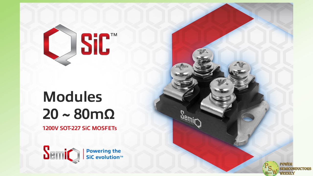
SemiQ announced that it has expanded its portfolio of QSiC™ Silicon Carbide modules with the launch of a family of 1200V MOSFETs that pairs with or without 1200V SiC Schottky Diodes in a SOT-227 package.
Crafted from high-performance ceramics and rigorously engineered to function with unwavering reliability in challenging conditions, the newly introduced SemiQ SiC modules achieve remarkably high performance. This enhanced performance empowers higher power densities and more streamlined design configurations.
The QSiC™ modules feature high breakdown voltage (> 1400 V), high-temperature operation (Tj = 175 °C), and low Rds(On) shift over the full operating temperature range while providing industry-leading gate oxide stability and gate oxide lifetime, avalanche (UIS) ruggedness, and extended short-circuit withstand times.
Target markets for the new QSiC™ modules with our existing SOT-227 SiC SBD modules include EV charging, on-board chargers (OBCs), DC-DC converters, E-compressors, fuel cell converters, medical power supplies, energy storage systems, solar and wind energy systems, data center power supplies, UPS/PFC circuits, and other automotive and industrial power applications.
All of the new QSiC™ modules are tested at wafer-level gate burn-in to provide high-quality gate oxide with stable gate threshold voltage. Besides the burn-in test, which helps to stabilize the extrinsic failure rate, stress tests such as gate stress, high-temperature reverse bias (HTRB) drain stress, and high humidity, high voltage, high temperature (H3TRB) to ensure requisite industrial grade quality levels.
Dr. Timothy Han, President at SemiQ, said, “We are delighted with the customer input and needs for our new family of QSiC™ high-power modules and thank our SemiQ team who have worked tirelessly to build and qualify our latest QSiC™ modules.”
SemiQ’s new 1200V SOT-227 modules are available in 20mΩ, 40mΩ, 80mΩ SiC MOSFET categories. A table with part numbers is shown below.
Part Numbers Circuit Configuration Ratings, Packages Rds(on), mΩ GCMX020B120S1-E1 Single MOSFET w/o SBD 1200V/113A, SOT-227 20 GCMS020B120S1-E1 Single MOSFET w SBD 1200V/113A, SOT-227 20 GCMX040B120S1-E1 Single MOSFET w/o SBD 1200V/57A, SOT-227 40 GCMS040B120S1-E1 Single MOSFET w SBD 1200V/57A, SOT-227 40 GCMX080B120S1-E1 Single MOSFET w/o SBD 1200V/30A, SOT-227 80 GCMS080B120S1-E1 Single MOSFET w SBD 1200V/30A, SOT-227 80 Original – SemiQ
-

Soitec announced its revenue for the second quarter of fiscal year 2024 and its results for the first half of fiscal year 2024 (ended on September 30th, 2023). The financial statements were approved by the Board of Directors during its meeting today.
- Q2’24 revenue reached €245m, down 7% at constant exchange rates and perimeter compared to Q2’23
- H1’24 revenue at €401m, down 15% both at constant exchange rates and perimeter and on a reported basis compared with H1’23 – in line with guidance
- H1’24 EBITDA margin stood at the robust level of 33% of revenue while the Company maintained significant investment in R&D
- Anticipated return to a slight year-on-year organic growth in H2’24, leading to a moderate downward revision of FY24 outlook: mid-single digit decline in FY’24 revenue expected at constant exchange rate and EBITDA1 margin2 anticipated around 35%
Pierre Barnabé, Soitec’s CEO, commented: “With a sequential growth of over 50% compared to the first quarter, our second-quarter revenue rebounded significantly, as we had anticipated. This was particularly the case in Mobile Communications as the inventory correction across the smartphone value chain eased. We continue to leverage strong demand in Automotive to deploy our SmartSiC™roadmap and we continue to progress actively with several customers.
Overall, our first half revenue is in line with our expectations. We have maintained strong profitability and a solid financial position, while continuing to invest in R&D and industrial capacity, as well as building inventories to prepare for H2’24.
Looking ahead, we maintain our growth perspectives for the second part of the fiscal year. We note however that the absorption of RF-SOI inventories at our customers level will last longer than anticipated. At the same time, we continue to expect sustained demand in Automotive & Industrial as well as in Smart Devices. Consequently, we now anticipate a full-fiscal-year revenue decline of around mid-single digit percentage, and an EBITDA margin of around 35%. After this transition year, we will resume our growth trajectory” added Pierre Barnabé.
FY’24 outlook
Soitec confirms growth recovery in the second half of FY’24. Against the backdrop of a weaker-than-expected smartphone market, the extent of the inventory correction at our customers level is greater than anticipated. We confirm strong traction for our Automotive & Industrial and Smart Devices divisions. We now anticipate our FY’24 revenue to slightly decline, by around a mid-single digit percentage, compared to FY’23, at constant exchange rates and perimeter.
As a result, FY’24 EBITDA margin is now expected to be around 35% of revenue. The Group will continue to implement cost control measures, while further investing significantly in R&D.
FY’24 Capital expenditure is expected to be around 290 million Euros in order to support growth beyond FY’24. Soitec’s growth outlook remain very strong: while the SOI content within end devices continues to increase, the ongoing penetration of the Group’s products across its three end markets and the successful deployment of its expansion into Compound Semiconductors with POI and SmartSiC™ becoming new significant growth drivers in the future.
Original – Soitec
-

The Hanau-based technology company Heraeus has acquired a significant stake in the start-up company Zadient. Heraeus, as a German high-tech materials player considers the market of SiC base material highly relevant and a suitable addition to its other operations.
The French-German firm Zadient specializes in the production of silicon carbide source material. Silicon carbide is a wide band gap semiconductor material, which is currently gaining rapid traction in the semiconductor market. Its properties lend themselves to use in power semiconductors, which help to convert current and voltages.
Its fundamental contribution is the dramatic increase in efficiency it provides over silicon by reducing the heat losses that occur while power passes through chips. Its ability to handle higher power densities with low losses allows for the transition from 400V to 800V battery systems in EVs which significantly shortens their charging time and increases their range. SiC based electronics are also smaller and lighter, which also contributes to increased range.
These properties have lead to the rapid adoption of SiC in applications ranging from the main inverters and on-board chargers in EVs to wind and solar power inverters, battery storage systems and even airplane power management modules. The breadth of these few examples is already an indication of the significant role SiC will play in the mobility and energy transition.
Through the partnership, Heraeus intends to accelerate the company’s growth and support Zadient’s innovative approach with its own know-how.
“Heraeus recognizes the potential of the SiC market and considers it to be highly relevant for high-tech applications. By acquiring a stake in Zadient, we can jointly offer our customers even better solutions” said Steffen Metzger, member of the Heraeus Group Management Committee. “We are very happy that we found a way to accelerate growth in the SiC market by combining the innovative ideas of the materials start-up Zadient with the manufacturing and technical expertise of the Heraeus Group.”
“We are very excited to be partnering with an industry leader like Heraeus,” noted Zadient CEO Kagan Ceran. “The expertise that Heraeus has in the industrial scale production of advanced materials, both in its home market of Germany and abroad, offers us unique synergies as we strive to realize our vision to be the world’s largest volume, highest purity producer of silicon carbide semiconductor materials.”
Original – Heraeus
-

Mitsubishi Electric Corporation announced that it will enter into a strategic partnership with Nexperia B.V. to jointly develop silicon carbide (SiC) power semiconductors for the power electronics market. Mitsubishi Electric will leverage its wide-bandgap semiconductor technologies to develop and supply SiC MOSFET chips that Nexperia will use to develop SiC discrete devices.
The electric vehicle market is expanding worldwide and is helping to drive the exponential growth of SiC power semiconductors, which offer lower energy loss, higher operating temperatures and faster switching speeds than conventional silicon power semiconductors. The high efficiency of SiC power semiconductors is expected to contribute significantly to global decarbonization and green transformation.
Mitsubishi Electric has established leading positions in applications such as high-speed trains, high-voltage industrial applications and home appliances. The company launched the world’s first SiC power modules for air conditioners in 2010 and became the first supplier of an all-SiC power module for Shinkansen bullet trains in 2015. Mitsubishi Electric has accumulated superior expertise for the development and manufacture of SiC power modules, which are known for their advanced performance and high reliability.
Going forward, Mitsubishi Electric expects to strengthen its partnership with Nexperia, a global leader with decades of experience in the design, manufacture, quality assurance and supply of diverse discrete devices. Nexperia’s devices are used in the automotive, industrial, mobile and consumer markets, contributing to decarbonization and a more sustainable future. Mitsubishi Electric will continue to improve the performance and quality of its SiC chips and focus on the development of power modules using proprietary module technologies.
Mark Roeloffzen, SVP & General Manager Business Group Bipolar Discretes at Nexperia, said: “This mutually beneficial strategic partnership with Mitsubishi Electric represents a significant stride in Nexperia’s silicon carbide journey. Mitsubishi Electric has a strong track record as a supplier of technically proven SiC device and modules. Combined with Nexperia’s high-quality standards and expertise in discrete products and packaging, we will certainly generate positive synergies between both companies – ultimately enabling our customers to deliver highly energy efficient products in the industrial, automotive or consumer markets they serve.”
Masayoshi Takemi, Executive Officer and Group President, Semiconductor & Device at Mitsubishi Electric, said: “Nexperia is a leading company in the industrial sector with proven technologies for high quality discrete semiconductors. We are delighted to enter into this co-development partnership that will leverage the semiconductor technologies of both companies.”
Original – Mitsubishi Electric
-
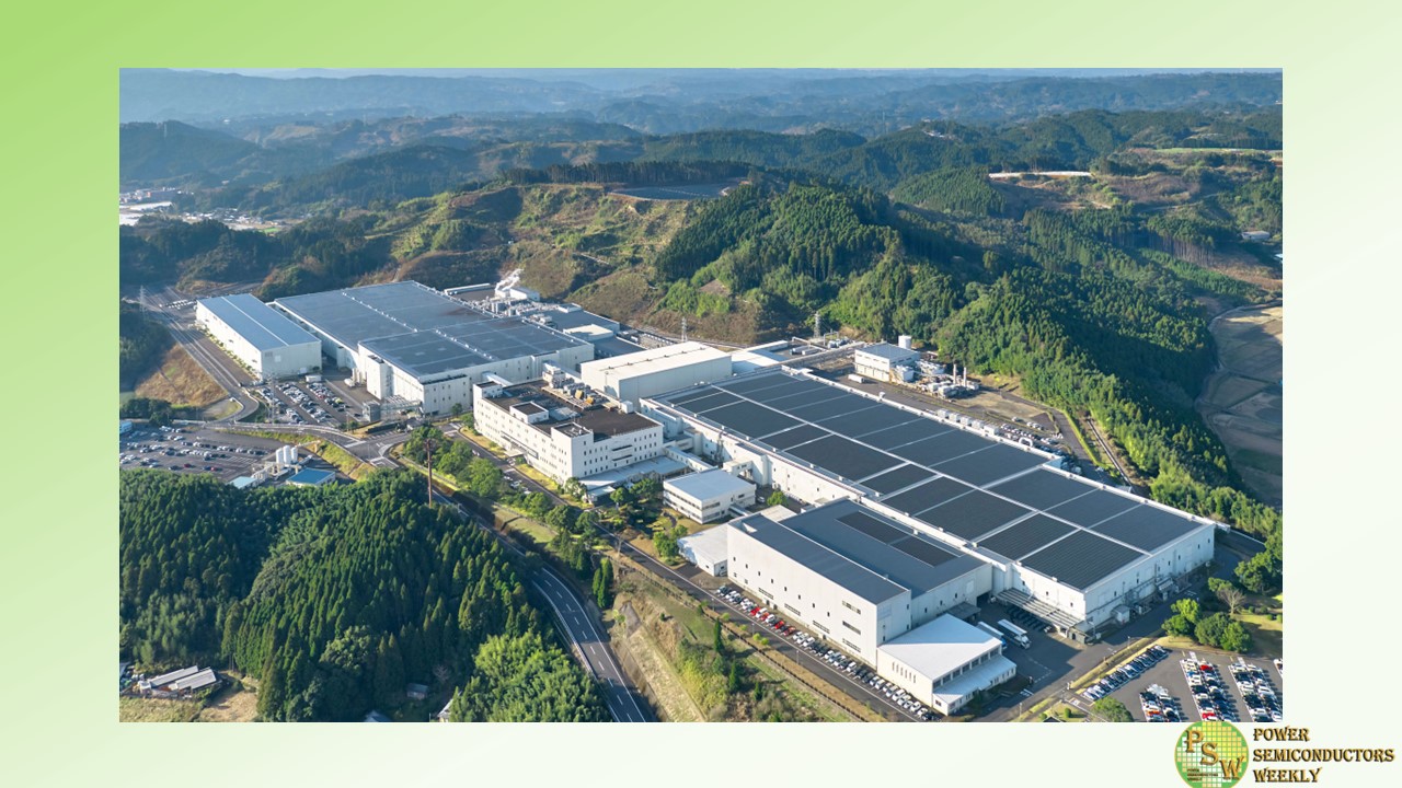
ROHM has completed the acquisition of the assets of Solar Frontier’s former Kunitomi Plant located in Japan, on November 7, 2023, based on its basic agreement signed with Solar Frontier.
The Plant will be operated by LAPIS Semiconductor, a subsidiary of the ROHM Group, as its Miyazaki Plant No.2. It will become the Group’s main production site for SiC power devices and is aiming to start operation during 2024.
The ROHM Group will continue to strengthen its production capacity in accordance with its Medium-Term Management Plan while keeping abreast of market conditions, and will also thoroughly enhance its BCM system to ensure a stable supply of products to customers.
Original – ROHM
-
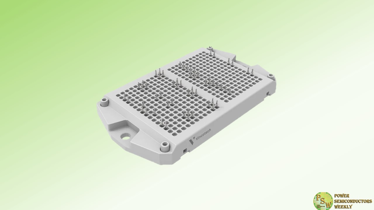
Engineered for maximum power density, this half-bridge module can serve to construct excellent H-bridges and sixpacks. Far higher current handling, enhanced power loss dissipation, greater scalability than a solution with a single-module footprint – the flowDUAL delivers all this and more.
In combination with VINcoPress and advanced die-attach technology, this new baseplate-less module from Vincotech is your first choice for a wide range of high-power use cases where utmost efficiency and reliability are top priorities.
Main benefits
- Outstanding, ≥99% conversion efficiency brings down overall costs
- Low stray inductance and symmetrical chip layout enable higher switching frequency and lower system costs
- Greater supply chain security with
– the new flow E3 industry standard-compatible housing (CTI >600)
– the latest multi-sourced SiC devices - Excellent thermal performance with VINcoPress technology to decrease junction temperature and increase lifetime
- Pre-applied PC-TIM rated for 150°C helps reduce production cost
Applications
- Industrial drives
- Embedded drives
- EV Chargers
- Solar
- UPS
Original – Vincotech
-
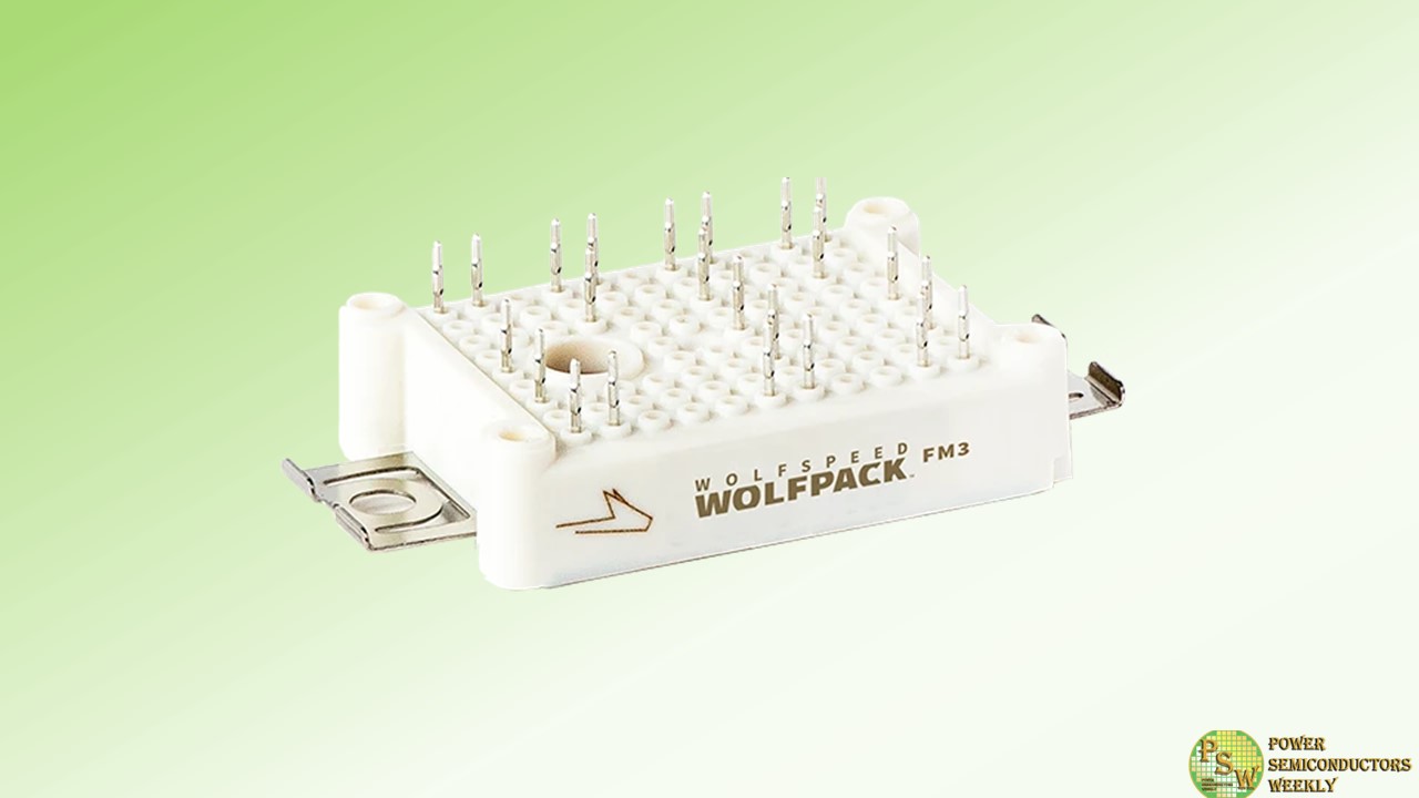
The Wolfspeed WolfPACK power module family is designed to give engineers choice and flexibility when working on power electronics applications greater than 10 kW.
In addition to half-bridge and six-pack topologies, WolfPACK modules are now available in full-bridge configurations—all with the option for pre-applied Honeywell™ PTM6000 Series TIM.
Selecting pre-applied TIM can reduce assembly cost and complexity, while improving reliability and performance. Compared to standard grease solutions, WolfPACK modules with pre-applied TIM can reduce the junction temperature by 40°C under the same conditions or increase current capability by 60% due to the reduction in thermal resistance.
All WolfPACK modules are designed to provide clean, reliable power for energy conversion systems. By leveraging more than 35 years of vertically integrated industry experience, Wolfspeed ensures that these modules offer low losses in a package that lends itself to fast design implementation, scalability, long term design support, and lower assembly overhead.
Original – Wolfspeed
-
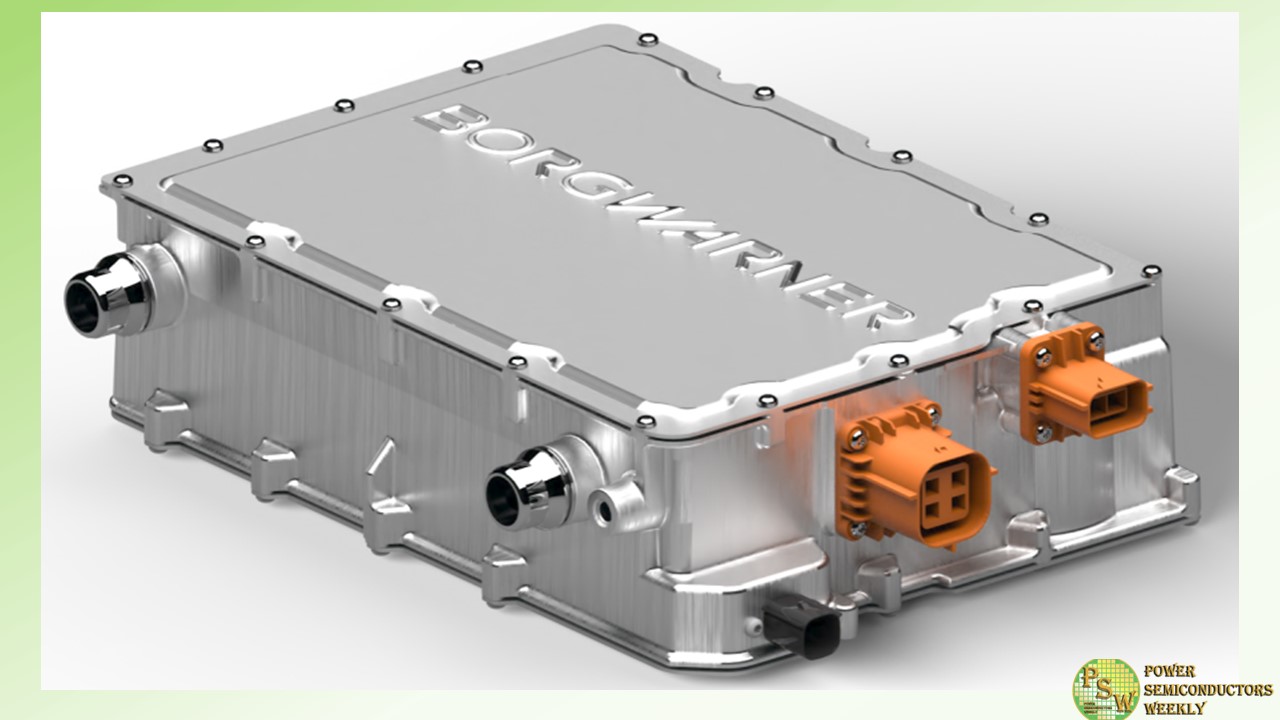
BorgWarner has clinched an agreement with a major North American OEM to supply its bi-directional 800V Onboard Charger (OBC) for the automaker’s premium passenger vehicle battery electric vehicle (BEV) platforms. The technology leverages silicon carbide (SiC) power switches for improved efficiency and delivers amplified power density, power conversion and safety compliance. Start of production is slated for January 2027.
“This is a big accomplishment for the team at BorgWarner, highlighting our first OBC win with this OEM and marks the first OBC win in North America,” said Dr. Stefan Demmerle, President and General Manager, BorgWarner PowerDrive Systems.
“Through our world-class power electronics expertise and market leading status for our 800-volt and silicon carbide technology, we are providing a solution to maximize charging power capabilities, extend power densities and enhance efficiencies while catering to differing grid configurations across regions.”
BorgWarner’s OBC technology is installed in electric vehicles to convert alternating current (AC) from the power grid to direct current (DC) to charge batteries. The OBC is capable of powers ranging from 19.2kW single-phase operation to 22kW three-phase operation.
The 19.2kW power level uses two power lines for a single-phase grid connection, which is unique to the U.S. market. The 22kW power level uses a three-phase grid connection and is intended for use in the European market. The 19.2kW single-phase charger is currently the only one of its kind to be introduced into the U.S. market.
The OBC incorporates a bi-directional vehicle-to-load (V2L) operating mode that enables users to use the vehicle battery pack to charge various standalone applications, which is an increasingly desired feature within the industry. Additionally, both the charger hardware and software are designed and produced by BorgWarner.
Original – BorgWarner
-
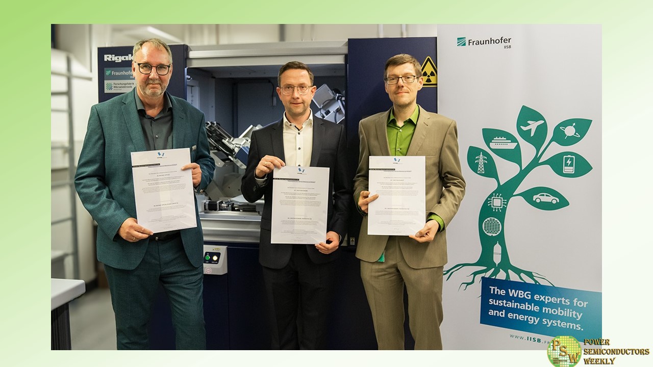
A cross-organizational team from Rigaku SE and Fraunhofer IISB has established a new semicon-ductor material characterization method in their jointly operated Center of Expertise for X-ray Topography in Erlangen, Germany. They succeeded not only in developing an industry-ready X-ray topography system, but also in employing defect detection and quantification algorithms, achieving a worldwide unique material characterization method for silicon carbide (SiC) wafers.
SiC is an excellent semiconductor for application areas like electric mobility and transportation, sustainable energy supply, industrial infrastructure up to sensors and quantum technologies even under harsh operating conditions.
As representatives for the whole research team, Dr. Kranert and Dr. Reimann from Fraunhofer IISB and Dr. Hippler, Managing Director Rigaku Europe SE, have won the Georg Waeber Innovation Award 2023 from the Förderkreis für die Mikroelektronik e.V. (Microelectronics Promotion Society).
Pioneering holistic material defect characterization with X-ray topography
In 2021, Rigaku SE and Fraunhofer IISB have founded the Center of Expertise for X-ray Topography, a joint lab that is located at the IISB’s headquarters in Erlangen, Germany. Here, the cross-organizational team has now developed a new metrology that is non-destructive, robust, reliable, high-throughput and therefore capable of swiftly detecting all relevant crystallographic defects in SiC substrates.
For the first time worldwirde, this innovation realized the holistic approach of setting up the measurement device, i.e., the X-ray topography (XRT) tool as well as formulating appropriate measurement and analysis routines that specifically meet the industry’s demands for speed, reliability, and accuracy. The development process was supported by rigorous scientific validation of the results, a crucial factor for the acceptance of a new approach in the industry.
Until now, no such industry-ready metrology existed for the early stages of SiC power electronics manufacturing, especially at substrate or crystal (commonly referred to as the “puck”) level. This breakthrough in SiC substrate inspection makes it no longer necessary to, e.g., destructively defect etch and discard semiconductor substrates for characterization, as is currently often the case. In consequence, the developed XRT metrology is superior to these existing substrate characterization methods employed in the industry, ultimately leading to substantial cost savings.
Effectively, this technology, developed in Germany, provides everything needed to become the industry standard for specifying and controlling substrate quality in production as well as for R&D substrate and device manufacturers worldwide. The success of this joint innovation is vividly illustrated by the new business, which Rigaku has successfully established in less than two years. Now, the Japan-based company is the world’s leading supplier of XRT tools for SiC substrate and device manufacturing.
The innovative metrology approach has been driven significantly by Dr. Michael Hippler, Managing Director of Rigaku Europe SE, and Dr. Christian Kranert with Dr. Christian Reimann, both group managers in the Fraunhofer IISB’s Materials department. Hence the scientists were selected for the Georg Waeber Innovation Award 2023 by the Förderkreis für die Mikroelektronik e.V. (Microelectronics Promotion Society).
The Förderkreis is an association of industry companies, two Fraunhofer institutes, four chairs of the University of Erlangen-Nuremberg and the Nuremberg Chamber of Commerce and Industry. The main objective is to foster a smooth exchange between science and industry, which is manifested in the Georg Waeber Innovation Award. The award is presented annually for outstanding scientific achievements and places a strong emphasis on the advancement of knowledge in microelectronics and its practical application in the industry. On October 25, 2023, Dr. Hippler, Dr. Reimann and Dr. Kranert received the award during a ceremony at Fraunhofer IISB in Erlangen.
Paving the way for the next generation of SiC power electronics
SiC semiconductor devices play a pivotal role in the power electronics industry. As a replacement for conventional silicon-based power electronics, SiC has the potential to enhance energy efficiency while reducing system costs. It is relevant across various application areas from electric mobility and transportation, sustainable energy supply, industrial infrastructure up to sensors and quantum technologies even under harsh operating conditions.
Consequently, processing low-cost, energy-efficient, and highly reliable SiC power devices is a critical endeavor with the worldwide electrification trend. The production capacities for SiC wafers experience significant growth, which goes hand in hand with an increasing demand for wafer inspection and metrology within the SiC industry. In particular, manufacturers of substrates and power devices require precice information regarding the quality of substrates in terms of crystallographic defects, their distribution across the entire wafer area, and absolute quantities.
Original – Fraunhofer IISB
