-

Axcelis Technologies, Inc. announced a shipment of the Company’s Purion EXE™ SiC high energy implanter as well as a successful Purion H200™ SiC medium energy implanter evaluation closure at leading power device chipmakers located in Japan. The systems will be used for 150mm and 200mm production of silicon carbide power devices supporting automotive, industrial, energy, and other power intensive applications.
Greg Redinbo, Executive Vice President, Marketing and Applications remarked, “The successful evaluation closure of the 200mm Purion H200 SiC system enables it to join an existing 200mm Purion EXE SiC in production at a leading power device customer in Japan.” Dr. Redinbo continued, “The shipment of an additional Purion EXE SiC to a new 150mm customer in Japan highlights growing customer requirements for even higher energy ion implant recipes on advanced SiC power devices, which the Purion Power Series provides.”
President and CEO, Russell Low commented, “We look forward to supporting our growing installed base in Japan and remain focused on expanding our market share by providing customers with the most innovative implant technology and support solutions to ensure their success. The Purion Power Series is the market leader due to its highly differentiated features and process control capabilities that are enabling for power device applications. Axcelis is the only ion implant company that can deliver complete recipe coverage for all power device applications.”
Original – Axcelis Technologies
-

Aehr Test Systems announced it has received an initial customer order for a FOX-NP™ wafer level test and burn-in system, multiple WaferPak™ Contactors, and a FOX WaferPak Aligner to be used for engineering, qualification, and small lot production wafer level test and burn-in of their silicon carbide devices.
The customer is multiple billion dollar per year global semiconductor company with locations across Europe, Asia, and the Americas that serves various industries including automotive, industrial, mobile, and consumer applications. The FOX-NP system, including the FOX WaferPak Aligner and initial WaferPaks, are scheduled to ship over the next few months.
The FOX-NP system is configured with the new Bipolar Voltage Channel Module (BVCM) and Very High Voltage Channel Module (VHVCM) options that enable new advanced test and burn-in capabilities for silicon carbide power semiconductors using Aehr’s proprietary WaferPak full wafer Contactors.
Gayn Erickson, President and CEO of Aehr Test Systems, commented, “We are very excited that this new customer selected our FOX-P solution for engineering, qualification, and production of their silicon carbide power devices. After working with the Aehr team and our technology solutions over an extended period of time, they felt secure in our ability to aid them in achieving these goals. A key feature in their selection of our FOX solution is its proven ability to cost-effectively implement their target burn-in and stabilization requirements, including 100% traceability and proof that every device on the wafer is burned in for the needed test duration.
“This customer currently has a wide range of automotive products and is entering the silicon carbide market to address several applications that include automotive, industrial, and electrification infrastructure. Key capabilities of our solution include our ability to scale from engineering and qualification and small lot production with the FOX-NP system to large scale production with the FOX-XP with Automated WaferPak Aligner. They have told us that they plan to transition to our FOX-XP multi-wafer test and burn-in systems for high-volume production. Aehr’s FOX-P technology facilitates a seamless transition from engineering to high-volume production with 100% compatibility between systems.
“This customer sees the enormous opportunity for silicon carbide power devices in industrial and power applications. William Blair forecasts that in addition to the 4.5 million six-inch equivalent wafers that will be needed to meet the demand for electric vehicle related silicon carbide devices in 2030, another 2.8 million wafers are needed to address industrial, solar, electric trains, energy conversion and other applications in 2030. The cost of ownership of our solution proves to be more cost-effective and efficient for these devices than package part burn-in after the die are packaged. This is a strong testimony of the advantage of wafer level burn-in as a better alternative to package part burn-in.
“The FOX family of compatible systems including the FOX-NP and FOX-XP multi-wafer test and burn-in systems and Aehr’s proprietary WaferPak full wafer contactors provide a uniquely cost-effective solution for burning in multiple wafers of devices at a single time to remove early life failures of silicon carbide devices, which is critical to meeting the initial quality and long-term reliability of the automotive, industrial, and electrification infrastructure industry needs.”
The FOX-XP and FOX-NP systems, available with multiple WaferPak Contactors (full wafer test) or multiple DiePakTM Carriers (singulated die/module test) configurations, are capable of functional test and burn-in/cycling of devices such as silicon carbide and gallium nitride power semiconductors, silicon photonics as well as other optical devices, 2D and 3D sensors, flash memories, magnetic sensors, microcontrollers, and other leading-edge ICs in either wafer form factor, before they are assembled into single or multi-die stacked packages, or in singulated die or module form factor.
Original – Aehr Test Systems
-
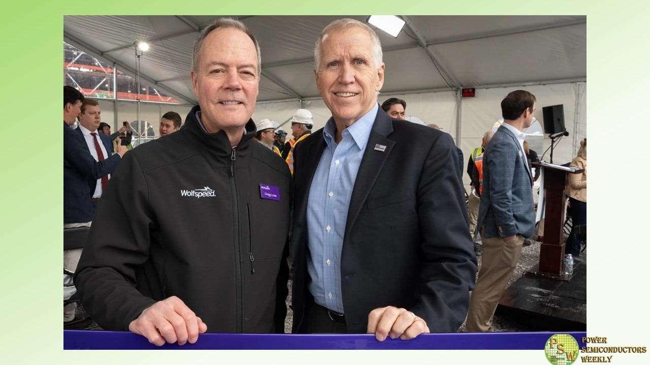
Wolfspeed, Inc. hosted Senator Thom Tillis (R-NC) and other local officials, community partners, and employees at a ceremony to celebrate the topping out of construction at the $5 billion John Palmour Manufacturing Center for Silicon Carbide. Located in Chatham County, North Carolina, the JP will produce 200mm silicon carbide wafers, significantly expanding Wolfspeed’s materials capacity, and meet the demand for next generation semiconductors critical to the energy transition and AI.
“We are excited to mark this critical milestone alongside our hard-working team, loyal customers, community partners, and ardent supporters like Senator Thom Tillis,” said Wolfspeed President and CEO, Gregg Lowe.
“This facility is a testament to Wolfspeed’s commitment to our local community and domestic workforce, furthering our position as the global leader in silicon carbide production. The JP will help maintain America’s lead in energy innovation, and unlock significant benefits for our local community by growing the state’s economy by more than $17.5 billion over the next two decades and creating 1,800 good-paying jobs by 2030.”
“Wolfspeed’s $5 billion investment in Chatham County is another example of why North Carolina is the best state in the country to do business,” said Senator Tillis. “I was proud to vote in favor of the CHIPS and Science Act, which provides critical support for domestic semiconductor manufacturing, and I applaud Wolfspeed’s commitment to developing technology here in North Carolina that supports our national security and economic interests.”
The JP represents a total investment of $5 billion, complemented by public and private support, to help accelerate the transition from silicon to silicon carbide and ramp up supply of this material recently deemed as critical to the energy transition by the U.S. Department of Energy. By the end of 2024, phase one of construction is expected to be completed on the 445-acre site.
The ramp of the JP will support recently signed customer agreements with Renesas, Infineon, and additional companies, while driving meaningful progress towards Wolfspeed’s long-term growth strategy. The JP will primarily produce 200mm silicon carbide wafers, which are 1.7x larger than 150mm wafers, translating to more efficient wafers and ultimately, lower costs. The JP underpins Wolfspeed’s vision of accelerating the adoption of silicon carbide semiconductors across a wide array of end-markets and unlocking a new era of energy efficiency.
Wolfspeed currently produces more than 60% of the world’s silicon carbide materials at its Durham, N.C. headquarters, and is engaged in a $6.5 billion capacity expansion effort to dramatically increase production.
Original – Wolfspeed
-
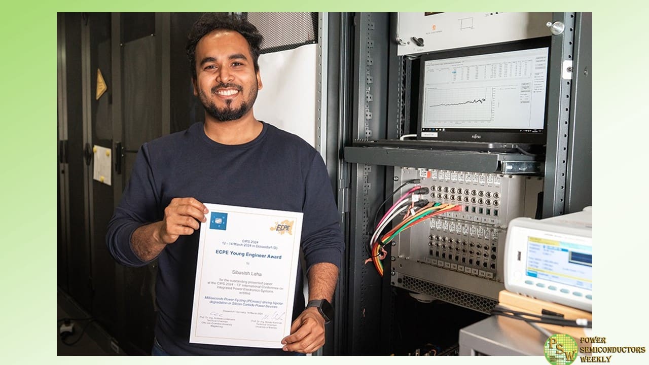
In the paper “Milliseconds Power Cycling (PCmsec) Driving Bipolar Degradation in Silicon Carbide Power Devices”, Sibasish Laha from Fraunhofer IISB and his co-authors Jürgen Leib, Andreas Schletz, Martin Maerz, Christian Liguda, Firas Faisal and Davood Momeni describe an innovative approach to silicon carbide (SiC) power cycling.
Until now, bipolar degradation (BD) tests have not been sufficiently differentiated in the investigation of failure and fault mechanisms for SiC power devices. SiC power products may experience voltage degradation which stems from the stacking faults (SFs) growth, commonly known as BD. To properly evaluate the BD impact on the electric performance of devices, it is important to distinguish it from other stress-related degradation such as power metal or interconnection.
This aspect has not yet been addressed, although the BD mechanism is well understood. The paper outlines a methodology by modifying the power cycling test (PCsec) to PCmsec in order to systematically investigate the effect of BD while controlling the impact of thermal degradation. This method enables a thorough evaluation of the distinct influences of both degradation contributors.
The complete paper will soon be available in the CIPS proceedings. Until then, feel free to download the paper presentation on event page.
There you can also find all our contributions to CIPS 2024:- Modified Approach for the Rainflow Counting Analysis of Temperature Load Signals in Power Electronics Modules – Oral presentation by S. Letz; Co-authors: D. Zhao, J. Leib, B. Eckardt, M. März
- Milliseconds Power Cycling (PCmsec) Driving Bipolar Degradation in Silicon Carbide Power Devices – Oral presentation by S. Laha; Co-authors: D. Momeni, J. Leib, A. Schletz, M. März, C. Liguda, F. Faisal
- Challenges of Junction Temperature Calibration of SiC MOSFETs for Power Cycling – a Dynamic Approach – Poster by J. Breuer, F. Dresel, A. Schletz, J. Klier, J. Leib, M. März, B. Eckardt
- Wide Bandwidth PCB Rogowski Coil Current Sensor with Droop Suppression and DC Restoration for In-Situ Inverter Measurements – Poster by S. Quergfelder, J. Sax, T. Heckel, B. Eckardt, M. März
Original – Fraunhofer IISB
-
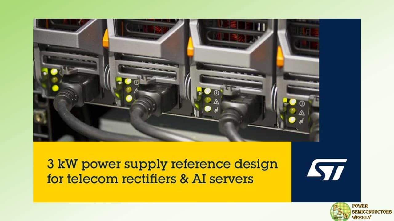
STMicroelectronics announced a collaboration with Compuware Technology Inc, (Compuware), a leading provider of high-efficiency power supplies, on a reference design for server power using ST’s industry-leading silicon carbide (SiC), galvanic isolation, and microcontroller technologies. This reference design provides unparalleled power-supply options for digital power converter applications including server, datacenter and telecom power.
As demand for digital services continues to grow, fueled by Artificial Intelligence (AI), 5G, and the Internet of Things (IoT), keeping power usage under control is an important piece of the sustainability puzzle for data centers. The STDES-3KWTLCP reference design is perfect for a 3kW and higher wattage CRPS (Common Redundancy Power Supply) server power supply. This technical advancement comes with superior efficiency, faster switching, reduced energy losses, and better thermal management capabilities. In addition, this total system solution shortens time-to-market.
Compuware stands as a global power supply leader, holding the world record for the highest number of 80 PLUS Titanium certifications, ensuring unparalleled power efficiency. Engineered for excellence, Compuware power solutions are the ideal choice for HPC, AI, Deep Learning, Cloud, and advanced applications. With high power density, it optimizes space usage without compromising reliability and efficiency, setting a new performance standard in demanding computing environments.
“Combining ST’s latest SiC MOSFET, galvanic isolation, and microcontroller technologies with Compuware’s leading-edge power energy expertise is helping Compuware unleash our design creativity to develop high-density and -efficiency solutions. Now we can achieve 89W/in.3 power density, a small size, and high power output, this reference design is a great choice for power-hungry, high-performance computing applications,” according to Robin Cheng, Vice President at Compuware.
“With a focus on the Industrial market, ST’s Power & Energy Competence Center provides low-power, mid-power, and high-power solutions with the most advanced ST technologies to our customers, and this reference design- STDES-3KWTLCP can help our customers increase energy efficiency and reduce time-to-market using ST’s efficient and reliable power solutions,” said Eric Chou, Head of Power & Energy Competence Center at STMicroelectronics.
Original – STMicroelectronics
-
 LATEST NEWS / SiC / WBG
Axcelis Technologies to Deliver Purion M™ SiC Implanters to Several Power Device Chipmakers in China
March 20, 2024
2 Min ReadAxcelis Technologies, Inc. announced multiple shipments of the Company’s Purion M™ SiC medium current implanter to several leading power device chipmakers located in China. The systems, which shipped in the first quarter, will be used for 150mm production of silicon carbide power devices supporting automotive, industrial, energy, and other power intensive applications.
President and CEO, Russell Low commented, “We look forward to supporting our customers as they expand their manufacturing capabilities in this growing silicon carbide power device segment. To meet market demand, chipmakers need to maximize their yield and add capacity, while meeting a range of technical challenges unique to power devices. The Purion M SiC Power Series platform’s common and flexible architecture, coupled with its uniquely differentiated high temperature capability, makes it ideally suited for this expanding application.”
Executive Vice President of Marketing and Applications, Greg Redinbo added “The Purion M SiC tool provides customers an implanter with a broad dose and energy range perfect for the early phases of a fab production ramp. The Purion M SiC sets the stage for the future introduction of the Purion H200™ SiC and Purion XE™ SiC. Use of the full Purion Power Series family enables higher fab productivity, lower cost of ownership and the ability to manufacture more advanced silicon carbide power devices.”
Original – Axcelis Technologies
-
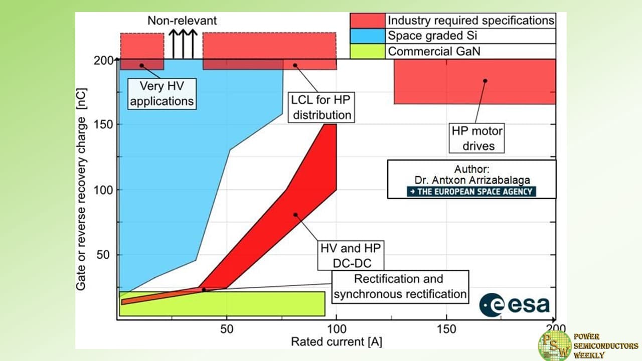
Recently the European Space Agency (ESA) started its search for the technological advantage to improve their systems. Lead by research fellow Dr. Antxon Arrizabalaga, the project is aimed at studying the latest semiconductor technologies and exploring the impact they can have in the future of the space industry.
During its research, Dr. Antxon Arrizabalaga is looking forward to answer the following questions:
- Which are the next system-level figures the space power industry wants to achieve?
- Can the wide bandgap semiconductors help to achieve these figures?
- Which semiconductor ratings are demanded by the space power industry for each application?
At the moment the research project lead by Dr. Arrizabalaga is focusing on the silicon carbide (SiC) power semiconductor devices, as they are better suited for the requirements of the high-power applications. The team has already had several meetings with the main European space power companies discussing the points of interest mentioned above.
As a result, ESA received rich feedback with industry requirements and new ideas. And as anticipated, most of the companies are looking to the ways to increase power of their systems.
Thus, the following applications were mentioned the most:
- Latching current limiters (LCL) for high power distribution
- High-voltage (HV), increasing the traditional bus voltage, and high-power (HP) DC-DC converters
- Rectification and synchronous rectification
- HP motor drives
- Very HV applications, around and over 1 kV
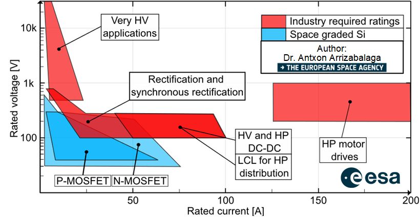
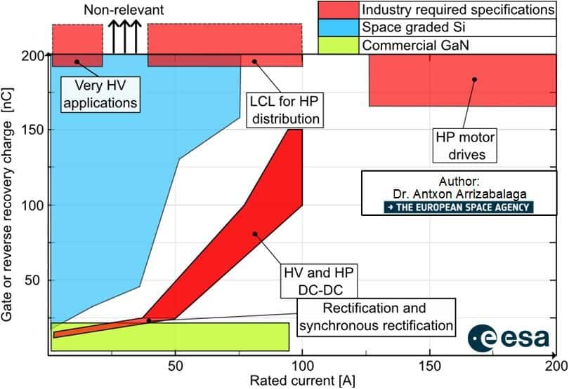
Figure 1. The ratings of the semiconductor devices required by the industry for each application
According to Dr. Arrizabalaga, ESA classifies innovations in three categories, according to the degree of innovation they bring when compared to the state-of-the-art:
- Enhancing. It brings a substantial improvement to the state-of-the-art system.
- Based on a technology replacement
- For SiC devices it means replacing the Si devices in an existing application and optimizing the system to get system-level benefits
- Low risk, development time and cost for manufacturers
- Straightforward adoption by industry and high probability of success
- Enabling. It will allow a new feature, new application, or even a new mission.
- Critical technologies for a certain feature, application or mission
- For SiC devices it means that without the adoption of such devices, the new desired feature, application or mission is no longer possible
- Medium-high risk for manufacturers, higher development cost and effort, since it has never been done before
- More challenging adoption by industry, and lower probability of success
- Game-changing. It promises to bring entirely new capabilities (not considered for this study).
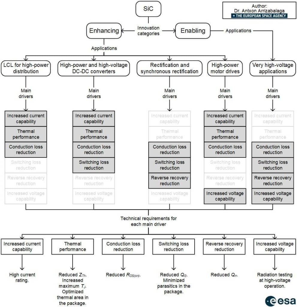
Figure 2. Classification of the applications mentioned by the industry and the main drivers needed to be optimized for each application.
The European Space Agency research team is looking forward to support the successful adoption of the wide bandgap (WBG) power semiconductor devices by the European space power industry, giving the European industry a competitive edge.
Original – Dr. Antxon Arrizabalaga
-
Infineon Technologies AG introduced the new CoolSiC™ MOSFETs 2000 V in the TO-247PLUS-4-HCC package to meet designers’ demand for increased power density without compromising the system’s reliability even under demanding high voltage and switching frequency conditions.
The CoolSiC MOSFETs offer a higher DC link voltage so that the power can be increased without increasing the current. It is the first discrete silicon carbide device with a breakdown voltage of 2000 V on the market and comes in a TO-247PLUS-4-HCC package with a creepage distance of 14 mm and clearance distance of 5.4 mm. With low switching losses, the devices are ideal for solar (e.g. string inverters) as well as energy storage systems and electric vehicle charging applications.
The CoolSiC MOSFET 2000 V product family is ideally suited for high DC link systems with up to 1500 V DC. Compared to 1700 V SiC MOSFETs, the devices also provide a sufficiently high overvoltage margin for 1500 V DC systems. The CoolSiC MOSFETs deliver a benchmark gate threshold voltage of 4.5 V and are equipped with a robust body diode for hard commutation. Due to the .XT connection technology, the components offer first-class thermal performance. They are also highly resistant to humidity.
In addition to the CoolSiC MOSFETs 2000 V, Infineon will soon be launching the matching CoolSiC diodes: The first launch will be the 2000 V diode portfolio in the TO-247PLUS 4-pin package in the third quarter of 2024, followed by the 2000 V CoolSiC diode portfolio in the TO-247-2 package in the final quarter of 2024. These diodes are particularly suitable for solar applications. A matching gate driver portfolio is also available.
The CoolSiC MOSFET 2000 V product family is available now. In addition, Infineon also offers a suitable evaluation board: the EVAL-COOLSIC-2KVHCC. Developers can use the board as a precise universal test platform to evaluate all CoolSiC MOSFETs and diodes 2000 V and the EiceDRIVER™ Compact Single Channel Isolated Gate Driver 1ED31xx product family through double pulse or continuous PWM operation.
Original – Infineon Technologies
-

Navitas Semiconductor announced their AI data center technology roadmap for up to 3x power increase to support similar exponential growth in AI power demands expected in just the next 12-18 months.
Traditional CPUs require typically only 300W and the data center ac/dc power supplies would typically power the equivalent of 10 of these or 3,000W (3kW). High-performance AI processors like NVIDIA’s ‘Grace Hopper’ H100 are already demanding 700W each today, with next-gen ‘Blackwell’ B100 & B200 chips anticipated to increase to 1,000W or more by next year.
To meet this exponential power increase, Navitas is developing server power platforms which rapidly increase from 3kW to up to 10kW. In August 2023, Navitas introduced a 3.2kW data center power platform utilizing latest GaN technology enabling over 100W/in3 and over 96.5% efficiency. Now, Navitas is releasing a 4.5kW platform enabled by a combination of GaN and SiC to push densities over 130W/in3 and efficiencies over 97%. These two platforms have already generated significant market interest with over 20 data center customer projects in development expected to drive millions in GaN or SiC revenues starting this year.
Today, Navitas also announces its plans to introduce an 8-10kW power platform by the end of 2024 to support 2025 AI power requirements. The platform will utilize newer GaN and SiC technologies and further advances in architecture to set all-new industry standards in power density, efficiency and time-to-market. Navitas is already engaged with major data-center customers, with full platform launch anticipated in Q4 ’24, completing this 3x increase in power demands in only 12-18 months.
Navitas’ unique data-center design center is creating these system designs to address the dramatic increases in AI data center power requirements, and assist customers to deploy platforms quickly and effectively to meet the accelerated time-to-market demands of rapid AI advances. System designs include complete design collateral with fully-tested hardware, schematics, bill-of-materials, layout, simulation and hardware test results to maximize first-time-right designs and fast revenue generation.
“The rapid development and deployment of artificial intelligence (AI) into global data centers has created a dramatic and unexpected power challenge for our entire industry,” noted Gene Sheridan, Navitas’ CEO and Co-Founder. “Our investment in leading-edge GaN and SiC technologies, combined with our unique data-center design center capabilities, have positioned us well. Our team has really stepped up to the challenge, with a 3x power increase in less than 18 months.”
Original – Navitas Semiconductor
-
 LATEST NEWS / PROJECTS / SiC / WBG
Tianjin Economic-Technological Development Area Inked Investment Agreement with Vitesco Technologies
1 Min ReadTianjin Economic-Technological Development Area (TEDA) inked an investment agreement with Vitesco Technologies for a new project for NEV intelligent manufacturing and automotive electronic products. With the new project, Vitesco aims to strengthen its presence in TEDA by introducing new products such as silicon carbide power modules, 800V motor stators and rotors, EMR3 three-in-one axle drive systems, high-voltage inverters, battery control units, and gearbox controllers.
Vitesco Technologies is a global leader in automotive technology development and manufacturing, dedicated to providing advanced driving technology for sustainable mobility. Vitesco Technologies has been cooperating with TEDA for many years.
The establishment of its R&D center in TEDA in 2019 marks a major step forward in the NEV market, upgrading the Vitesco Tianjin Base into a super factory integrating R&D, testing, and production. Thomas Stierle, member of the Executive Board and head of Electrification Solutions Division of Vitesco Technologies, expressed confidence in China, Tianjin, and TBNA. He stated that Vitesco Technologies will continue to increase its investment in TBNA and deepen cooperation in manufacturing R&D and technological innovation.
