-

MCC Semi announced the latest innovation in their MOSFET lineup. The 100V wide SOA MCTL2D0N10YHR with split-gate trench technology satisfies the design demands of high-performance applications with ease. Balancing efficiency and reliability in harsh conditions is no longer an issue, thanks to this N-channel power MOSFET’s wide safe operating area (SOA) and a host of efficient characteristics.
This SOA comparison highlights significant differences in drain current between two 100V MOSFETs, MCTL300N10YB and MCTL2D0N10YHR, at 10ms pulse. This MOSFET’s wide SOA enhances safety and performance while overcoming common challenges engineers face when designing for high-power applications. It also provides a host of features that add up to ultimate efficiency and reliability. With a gate charge and on-resistance of 2mΩ, this MOSFET also optimizes energy use at every angle, reducing operational costs.
Designed to withstand junction temperatures of up to 175⁰C, this component delivers unquestionable performance in environments where lesser components would fail. Excellent thermal management is also assured, thanks to the TOLL package engineered for superior heat dissipation, which mitigates thermal-related issues. MCC’s 100V MOSFET is the ideal solution for diverse applications, including telecommunications, computing, audio amplification, and motor controls.
Features & Benefits:
- Wide SOA: Ensures safe operation across a broad range of conditions.
- Split-gate Trench (SGT) Technology: Provides enhanced performance and efficiency.
- Low On-Resistance: Maximizes efficiency by minimizing power losses.
- Low Conduction Losses: Reduces heat generation during operation.
- Low Gate Charge: Maximizes efficiency by minimizing switching losses.
- Low Gate Charge: Maximizes efficiency by minimizing switching losses.
- Excellent Thermal Performance: TOLL package facilitates superior heat dissipation.
Original – Micro Commercial Components
-

Vishay Intertechnology, Inc. introduced two new IGBT and MOSFET drivers in the compact, high isolation stretched SO-6 package. Delivering high peak output currents of 3 A and 4 A, respectively, the Vishay Semiconductors VOFD341A and VOFD343A offer high operating temperatures to +125 °C and low propagation delay of 200 ns maximum.
Consisting of an AlGaAs LED optically coupled to an integrated circuit with a power output stage, the optocouplers are intended for solar inverters and microinverters; AC and brushless DC industrial motor control inverters; and inverter stages for AC/DC conversion in UPS. The devices are ideally suited for directly driving IGBTs with ratings up to 1200 V / 100 A.
The high operating temperature of the VOFD341A and VOFD343A provides a higher temperature safety margin for more compact designs, while their high peak output current allows for faster switching by eliminating the need for an additional driver stage. The devices’ low propagation delay minimizes switching losses, while facilitating more precise PWM regulation.
The optocouplers’ high isolation package enables high working voltages up to 1.140 V, which allows for high voltage inverter stages, while still maintaining enough voltage safety margin. The RoHS-compliant devices offer high noise immunity of 50 kV/µs, which prevents fail functions in fast switching power stages.
Original – Vishay Intertechnology
-

Toshiba Electronic Devices & Storage Corporation has expanded the lineup of 150V N-channel power MOSFETs with new six products that use the new generation process “U-MOSⅩ-H series.” Products in this series are suitable for the switching power supplies of industrial equipment such as data centers and communication base. The package of new products is a three-pin through hole type: TO-220 for “TK4R9E15Q5, TK7R2E15Q5 and TK9R6E15Q5” and TO-220SIS for “TK5R0A15Q5, TK7R4A15Q5 and TK9R7A15Q5.”
The new products use the U-MOSⅩ-H process to achieve low drain-source On-resistance. In particular, TK4R9E15Q5 features the excellent low drain-source On-resistance of 4.9mΩ (max). In addition, the new products uses high-speed diode (HSD) to improve reverse recovery characteristics, which are important for synchronous rectification applications, by reducing reverse recovery charge and faster reverse recovery time. Used in synchronous rectification applications, the new products reduce the power loss of switching power supplies and help improve efficiency.
The first product TPH9R00CQ5 which uses HSD, has approximately 74% less reverse recovery charge and approximately 44% faster reverse recovery time than Toshiba‘s existing product TPH9R00CQH, which does not use HSD. The U-MOSⅩ-H process using this HSD has applied to through hole type packages in addition to surface mount type packages.
The new products have reduced the drain source spike voltage generated between the drain and source when MOSFET is switching, helping to lower EMI in switching power supplies.
Toshiba will continue to promote the expansion of its power MOSFET lineup, which helps improve the efficiency of power supplies, thereby contributing to reducing the power consumption of equipment.
Applications
- Switching power supplies for communication equipment, etc. (high efficiency AC-DC converters, high efficiency DC-DC converters, etc.)
- Motor control equipment (motor drives, etc.)
Features
- Excellent low On-resistance:
TK4R9E15Q5 RDS(ON)=4.9mΩ (max) (VGS=10V) - Low reverse recovery charge:
TK9R6E15Q5 Qrr=32nC (typ.) (-dIDR/dt=100A/μs) - Fast reverse recovery time:
TK9R6E15Q5 trr=40ns (typ.) (-dIDR/dt=100A/μs)
Original – Toshiba
-

Affordability combined with high performance and efficiency is the key to making electric mobility accessible to a broader market. That’s why Infineon Technologies AG is introducing the HybridPACK™ Drive G2 Fusion, establishing a new power module standard for traction inverters in the e-mobility sector.
The HybridPACK Drive G2 Fusion is the first plug’n’play power module that implements a combination of Infineon’s silicon and silicon carbide (SiC) technologies. This cutting-edge solution provides an ideal balance between performance and cost efficiency, giving more choice in the optimization of inverters.
One of the main differences between silicon and SiC in power modules is that SiC has a higher thermal conductivity, breakdown voltage and switching speed, making it more efficient, but also more expensive than silicon-based power modules. With the new module, the SiC content per vehicle can be reduced, while maintaining vehicle performance and efficiency at a lower system cost. For example, system suppliers can realize nearly the system efficiency of a full SiC solution with only 30 percent SiC and 70 percent silicon area.
“Our new HybridPACK Drive G2 Fusion module underlines Infineon’s innovation leadership in the automotive semiconductor industry,” said Negar Soufi-Amlashi, Senior Vice President & General Manager High Voltage at Infineon’s Automotive division. “Addressing the demand for greater e-mobility range, this technological breakthrough smartly combines silicon carbide and silicon. Integrated in a well-introduced module package footprint it offers compelling cost-performance ratio over pure silicon carbide modules without adding system complexity for automotive system suppliers and vehicle manufacturers.”
HybridPACK Drive G2 Fusion expands Infineon’s HybridPACK Drive power module portfolio and can be quickly and easily integrated in vehicle components or modules without requiring complex adjustments or configurations. The HybridPACK Drive G2 Fusion module features up to 220 kW in the 750 V class. It ensures high reliability over the entire temperature range from -40 °C to +175 °C and improved thermal conductivity.
The unique properties of Infineon’s CoolSiC™ technology and its silicon IGBT EDT3 technology with very fast turn-on enable the use of a single gate driver or dual gate drivers. This allows easy re-design from full silicon or full SiC based inverters to a fusion inverter. Generally, Infineon’s holistic expertise in SiC MOSFET and silicon IGBT technology, power module packaging, gate drivers as well as sensors enables premium products with cost savings at system level. One example is the integration of Swoboda or XENSIV™ Hall sensors in the HybridPACK Drive package for more precise and efficient motor control.
Infineon will showcase the new HybridPACK Drive G2 Fusion at electronica 2024 in Munich from November 12 to 15 (hall C3, booth 502).
Original – Infineon Technologies
-

For next-generation power electronics, BASF has developed a polyphthalamide (PPA) that is especially suited for manufacturing housings of IGBT (insulated-gate bipolar transistor) semiconductors. Ultramid® Advanced N3U41 G6 addresses the growing demand for high-performance, reliable electronic components for e.g., electric vehicles, high-speed trains, smart manufacturing and the generation of renewable energy.
Semikron Danfoss, a global technology leader in power electronics, now uses the BASF PPA as housing in its Semitrans 10 IGBT which can be installed in inverters of photovoltaic and wind energy systems. Due to its outstanding chemical resistance and dimensional stability, the Ultramid® Advanced N grade enhances the robustness, long-term performance and reliability of these IGBTs, thus meeting growing needs for energy saving, higher power density and increased efficiency. IGBTs enable efficient switching and control of electrical circuits in power electronics.
“IGBTs are a key element of modern electronics, particularly in the renewable energy sector,” explains Jörn Grossmann from research and predevelopment at Semikron Danfoss. “IGBTs must operate at higher temperatures while maintaining long-term stability and performance. The Semitrans 10 has set a new benchmark for performance and efficiency benefiting from the unique properties of BASF’s PPA. We chose this material because of its extraordinary electrical isolation even in harsh environments and because of its excellent robustness against short-term temperature peaks in the assembly process.” The combination of high-performance material and smart design allows for faster switching speeds, lower conduction losses, and improved thermal management, thus addressing key needs in power electronics.
In today’s IGBTs, BASF’s proven Ultradur® (PBT: polybutylene terephthalate) is widely used. The new PPA is designed to meet the stringent requirements of next-generation IGBTs for rapidly evolving power electronics. They demand materials that can withstand higher temperatures, provide sustained electrical insulation, and maintain dimensional stability under challenging environmental conditions like humidity, dust and dirt.
The laser-sensitive Ultramid® Advanced N3U41G6 with non-halogenated flame retardant combines high thermal stability with low water uptake and excellent electrical properties. It is characterized by a high CTI (Comparative Tracking Index) of 600 (acc. to IEC 60112): This supports miniaturization of IGBTs by lower creepage and better insulation than materials so far used for power switches. The UL-certified grade shows an excellent electrical RTI (Relative Temperature Index) value of 150°C.
“BASF’s PPA compound is globally available and ready for sampling”, says Jochen Seubert, senior application expert for power electronics at BASF. “Backed by our customer-focused technical support in part development, we expect this innovative material to significantly contribute to the advancement of power electronics, supporting the global transition to renewable energies.” For manufacturing of IGBTs, the BASF PPA is compatible with potting materials used to assemble the semi-conductors with metal pins and clamps after injection molding.
BASF’s polyphthalamide portfolio is based on the six polymers Ultramid® Advanced N (PA9T), Ultramid® Advanced T1000 (PA6T/6I), Ultramid® Advanced T2000 (PA6T/66), Ultramid® T KR (PA6T/6), Ultramid® T6000 (PA66/6T) and Ultramid® T7000 (PA/PPA). They open the door to the next generation of lightweight, high-performance plastic components in many different sectors including the automotive industry, electronics and electric devices, mechanical engineering and consumer goods.
The PPA portfolio is available globally and complemented by BASF’s Ultrasim® simulation tool and extensive experience in application development. It includes more than 50 compounded grades for injection molding and extrusion, products with or without flame retardants. The compounds are available in different colors, from colorless to laser-markable black, with short-glass, long-glass or mineral fiber reinforcement, and with various heat stabilizers.
Original – BASF
-

Navitas Semiconductor announced GaNSlim™, a new generation of highly-integrated GaN power ICs that will further simplify and speed the development of small form factor, high-power-density applications by offering the highest level of integration and thermal performance.
GaNSlim enables the simplest, fastest, and smallest system design by integrating drive, control, and protection, with integrated EMI control and loss-less current sensing, all within a high thermal performance proprietary DPAK-4L package. Additionally, with an ultra-low startup current below 10 µA, GaNSlim devices are compatible with industry-standard SOT23-6 controllers and eliminate HV startup.
Integrated features such as loss-less current sensing eliminate external current sensing resistors and optimize system efficiency and reliability. Over-temperature protection ensures system robustness and auto sleep-mode increases light and no-load efficiency. Autonomous turn-on/off slew rate control maximizes efficiency and power density while reducing external component count, system cost and EMI.
GaNSlim features a patented, 4-pin, high-thermal-performance, low-profile, low-inductance, DPAK package. This package enables 7 °C lower temperature operation versus conventional alternatives, supporting high-power-density designs with ratings up to 500 W. Target applications include chargers for mobile devices and laptops, TV power supplies, lighting, etc.
“Our GaN focus is on integrated devices that enable high-efficiency, high-performance power conversion with the simplest designs and the shortest possible time-to-market,” says Reyn Zhan, Sr. Manager of Technical Marketing. “Our new GaNSlim portfolio – built on integration, ease-of-use, and low-cost manufacturing methods, – continues to grow the customer pipeline with over 50 new projects already identified. GaNSlim increases our GaN addressable market by enabling lower system costs compared to silicon designs for many applications, targeting applications under 500 W across mobile, consumer and home appliance.”
Devices in the NV614x GaNSlim family are rated at 700 V with RDS(ON) ratings from 120 mΩ to 330 mΩ and are available in versions optimized for both isolated and non-isolated topologies.
As with other Navitas GaN ICs, GaNSlim devices are supplied with an industry-leading twenty-year warranty, while demo boards for QR flyback, single-stage PFC, boost PFC plus QR flyback and TV power supply designs allow for rapid evaluation and selection of the optimum device for a given application.
Original – Navitas Semiconductor
-

MCC Semi unveiled the latest selection of 5000W TVS diodes designed to provide superior protection against transient voltage spikes. Whether caused by lightning or other electrical disturbances, voltage surges can add up to costly damage and system failures without proper safeguards in place. That’s where our 5000W TVS solutions come in.
With a broad range of voltages — from 11V to 400V — and a compact yet powerful SMC package, these transient voltage suppressors (TVS) optimize space on the board without sacrificing performance.
Leveraging glass-passivated junction technology, these TVS diodes ensure the highest durability and reliability in demanding environments at operating junction temperatures of up to 175°C. They also boast IEC 61000-4-2 ESD ratings of 30kV for air and contact discharge for enhanced protection during electrostatic discharge events.
Rapid response times with capacitance typically less than 3,000 pF and impressive clamping capabilities assure sensitive electronic components are adequately protected, and a leakage current less than 2µA above 11V reduces power losses.
Available in unidirectional and bidirectional configurations, MCC’s 5000W TVS diodes meet diverse application needs while reducing maintenance costs and boosting overall reliability.
Features & Benefits:
- IEC 61000-4-2 ESD Protection: 30kV (Air) and 30kV (Contact) for solid electrostatic discharge protection.
- Maximum Operating Junction Temperature: Rated up to 175°C for reliable operation in high-temperature environments.
- Ultra-Fast Response Time: Capacitance typically less than 3000 pF from 0V to breakdown voltage minimum, ensuring immediate protection.
- Low Leakage Current: Typical ID less than 2µA from 11V to minimize power loss.
Original – Micro Commercial Components
-

In battery-powered applications such as motor drives and switched-mode power supplies (SMPS), the power supply architecture often requires that a module can be disconnected from the main supply rail when a fault occurs in that module. To achieve this functionality, it is common to use high-side disconnect switches (e.g. MOSFETs) to prevent a load short circuit from affecting the battery.
Infineon Technologies AG introduced the EiceDRIVER™ 1EDL8011, a high-side gate driver designed to protect battery-powered applications such as cordless power tools, robotics, e-bikes, and vacuum cleaners in the event of a fault.
The device provides fast turn-on and turn-off of high-side N-channel MOSFETs with its high gate current capabilities. It consists of an integrated charge pump with an external capacitor to provide strong start-up. The internal charge pump provides the MOSFET gate voltage when the operating input voltage is low. The gate driver IC manages inrush current and provides fault protection. Undervoltage Lockout (UVLO) protection at input voltage prevents the device from operating under hazardous conditions. The driver is available in a DSO-8 package, making it ideal for space-constrained designs. It includes overcurrent protection (OCP), adjustable current setting threshold, time delay and a safe start-up mechanism with flexible blanking during MOSFET turn-on transitions.
The 1EDL8011 has a wide operating voltage range of 8 V to 125 V and a high gate sinking current of up to 1 A, allowing for efficient switching. Additionally, the product has an extremely low off-mode quiescent current of 1 µA, helping to minimize power consumption in sleep mode. The device also includes a V DS sense feature that is used to trigger an overcurrent shutdown by monitoring the drain-to-source voltage of the disconnect MOSFET.
Infineon will be showcasing a demo featuring the 1EDL8011 at its global technology forum OktoberTech™ 2024 in Silicon Valley on 17 October. The 1EDL8011 is available now. Further information can be found at www.infineon.com/1edl8011.
Original – Infineon Technologies
-
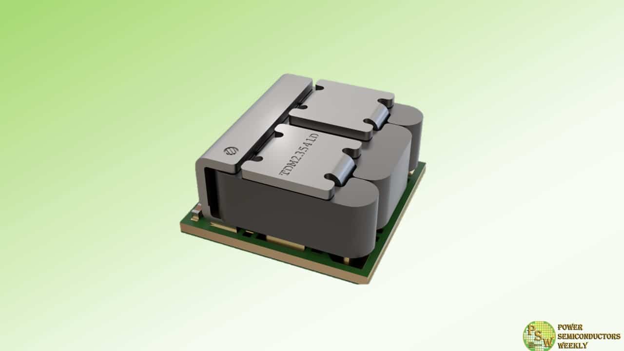
Data centers are currently responsible for more than two percent of global energy consumption. Fueled by AI, this number is expected to grow to up to around seven percent in 2030, matching the current energy consumption of India. Enabling efficient power conversion from grid-to-core is vital to enable superior power densities and thereby advance compute performance while reducing total cost of ownership (TCO).
Infineon Technologies AG is therefore launching the TDM2354xD and TDM2354xT dual-phase power modules with best-in-class power density for high-performance AI data centers. These modules enable true vertical power delivery (VPD) and offer industry’s best current density of 1.6 A/mm2. They follow the TDM2254xD dual-phase power modules introduced by Infineon earlier this year.
“We are proud to enable high-performance AI data centers with our TDM2354xT and TDM2354xD VPD modules. These devices will maximize system performance with Infineon’s trademark quality and robustness, thereby enabling best TCO for data centers,” said Rakesh Renganathan, Vice President Power ICs at Infineon Technologies. “Our industry-leading power devices and packaging technologies, combined with our extensive systems expertise, will further advance high-performance and green computing as part of our mission to drive digitalization and decarbonization.”
The TDM2354xD and TDM2354xT modules combine Infineon’s robust OptiMOS™ 6 trench technology, a chip-embedded package that enables superior power density through enhanced electrical and thermal efficiencies, and a new inductor technology to enable lower profile and therefore, true vertical power delivery.
As a result, the modules set new standards in power density and quality to maximize the compute performance and efficiency of AI data centers. The TDM2354xT modules support up to 160 A and are the industry’s first Trans-Inductor Voltage Regulator (TLVR) modules in a small 8 x 8 mm² form factor. Combined with Infineon’s XDP™ controllers, they offer extremely fast transient response and minimize on-board output capacitance by up to 50 percent, further increasing system power density.
The new modules will be showcased at Infineon’s global technology forum OktoberTech™ 2024 in Silicon Valley on 17 October and at electronica 2024 in Munich from November 12 to 14 (hall C3, booth 502).
Original – Infineon Technologies
-

Navitas Semiconductor announced that its high-power GaNSafe family is now available in a TOLT (Transistor Outline Leaded Top-side cooling) package.
The GaNSafe family has been specifically created to serve demanding, high-power applications, such as AI data centers, solar/energy storage, and industrial markets. Navitas 4th generation integrates control, drive, sensing, and critical protection features that enable unprecedented reliability and robustness. GaNSafe is the world’s safest GaN with short-circuit protection (350ns max latency), 2kV ESD protection on all pins, elimination of negative gate drive, and programmable slew rate control. All these features are controlled with 4-pins, allowing the package to be treated like a discrete GaN FET, requiring no VCC pin.
The TOLT packaging enhances thermal dissipation through the top side of the package, allowing heat to be dissipated directly to the heatsink (not through the PCBA). This enables the reduction of operating temperature and increases current capability, resulting in the highest level of system power density, efficiency, and reliability.
“With over 200 million units shipped and supplied with a 20-year warranty, Navitas’ highly integrated high-power GaNSafe ICs are proven to deliver performance and reliability while simplifying Design-IN for systems up to 22kW,” says Charles Bailley, Senior Director of Business Development. “As the most protected, reliable, and safe GaN devices in the industry, GaNSafe took our technology into mainstream applications above 1kW. Now, with the enhanced thermal dissipation of the TOLT package, we are enabling customers to deliver even better performance, efficiency, power density, and reliability in even the most demanding applications.”
Suitable for applications from 1 kW to 22 kW, 650 V GaNSafe in TOLT packaging is available with a range of RDS(ON)MAX from 25 to 98 mΩ. Integrated features and functions include:
- High-speed short-circuit protection, with autonomous ‘detect and protect’ with ultra-fast 350 ns / 50 ns latency.
- Protected, regulated, integrated gate-drive control, with zero gate-source loop inductance for reliable high-speed 2 MHz switching capability to maximize application power density.
- Electrostatic discharge (ESD) protection of 2 kV, compared to zero for discrete GaN transistors.
- 650 V continuous, and 800 V transient voltage capability for extraordinary application conditions.
- Integrated Miller Clamp (no negative gate bias, higher 3rd quadrant efficiency)
- Programmable turn-on and turn-off speeds (dV/dt) to simplify EMI regulatory requirements.
- Simple 4-pin device, allowing the package to be treated like a discrete GaN and requiring no additional VCC pin
- Robust, thermally enhanced packaging: ultra-low RQ_JUNC-AMB and board-level thermal cycling (BLTC) Reliability
In addition to the new ICs, Navitas will be offering reference design platforms based on GaNSafe TOLT for applications including data center power supplies and EV on-board chargers. These system platforms include complete design collateral with fully tested hardware, embedded software, schematics, bill-of-materials, layout, simulation, and hardware test results.
Original – Navitas Semiconductor
