-
Abstract
The silicon carbide (SiC) inverter brings great advantages to the motor drive systems of new energy vehicles; however, severe challenges to the bearings also happen. The high dc bus voltage and switching frequency of SiC inverter can increase the discharge frequency and energy when the bearing grease film collapses.
As a result, the bearing suffers severe electric corrosion, and the service life of the motor drive system can be shortened. In this paper, the characteristics of common-mode voltage and bearing voltage are analyzed, firstly under space vector pulse width modulation (SVPWM). After that, the common-mode equivalent circuit model of the motor drive system is established. The frequency characteristics of bearing voltage are revealed, and the safe working area is determined.
Then, the frequency characteristics of bearing voltage and current are verified based on IGBT and SiC inverters in experiments. After that, by designing a common-mode filter, the bearing voltage and current are significantly attenuated. Furthermore, the active zero state PWM (AZSPWM) is adopted to reduce the common-mode voltage from the inverter.
At the same time, combined with the common-mode filter, the bearing voltage and current are further reduced. The experimental results show that the switching frequency has a decisive effect on the amplitude of bearing voltage and current. The bearing voltage can be attenuated to around half of the reference bearing voltage by using the common-mode filter and AZSPWM strategy, respectively. T
he combination of the common-mode filter and AZSPWM strategy can reduce the bearing voltage to around one-fourth of the reference bearing voltage, which can effectively reduce the breakdown time and discharge energy of the grease oil film.
1. Introduction
The bearing is the key component which determines the life and reliability of the motor drive system. Motor failures are largely attributed to damage to the bearing, and electric corrosion is one of the main factors. Considering the complexity and cost, the three-phase, two-level voltage source inverter is mainly adopted in the electric vehicle drive system.
The common-mode voltage of the inverter couples through the parasitic capacitances of the motor, resulting in bearing voltage on both sides of the bearing lubricating grease oil film. When the bearing voltage exceeds the breakdown threshold of the lubricating grease oil film, the discharge phenomenon occurs, leading to the electric discharge machining (EDM) bearing current.
The energy released during the discharge can cause concave pits on the surface of inner and outer rings as well as on the rolling balls of the bearing. A large number of breakdown discharges can cause great damage to the bearing, posing a serious threat to the life of the motor drive system.
The 800 V dc bus voltage and SiC power devices are becoming the development direction for electric vehicle drive systems. The high voltage and high frequency are conducive to the reduction in the volume and the improvement of the power density of motor drive systems. For example, in 2022, Marelli Europe S.p.A., a well-known auto parts supplier, developed a high power density SiC inverter with a dc bus voltage of 900 V and a switching frequency of 65 kHz.
Compared with the traditional IGBT inverters, its volume and weight were reduced by 30%, the loss was reduced by 50%, and the efficiency reached 99.5%. The National New Energy Vehicle Technology Innovation Center also developed an SiC inverter with a dc bus voltage 900 V in 2022, with the capacity of 550 kVA and a switching frequency of 25 kHz. Compared with the traditional design, the volume was reduced by 6.6 times, and the weight was reduced by 3.3 times.
However, the increase in dc bus voltage and switching frequency could exacerbate the bearing electric corrosion. Bearing electric corrosion has become a pain point problem that needs to be solved urgently in the field of electric vehicles.
From current research, it could be summarized that the suppression of the motor bearing current can be addressed from three aspects, including the bearing reinforcement, the capacitive coupling paths within the motor, and the source of common-mode voltage. Conductive grease bearings and ceramic bearings have been applied to suppress bearing current. Conductive grease bearings create a conductive channel inside the bearing, bypassing the bearing oil film, making it difficult to establish a stable bearing voltage, which prevents the discharge of the bearing oil film.
However, the metallic particles in the lubricating grease can increase its mechanical wear. Additionally, designing a lubricating grease that balances both lubrication and conductivity poses a technical challenge. Ceramic bearings employ the insulating method to block the current path, increasing the bearing impedance to suppress the bearing current. However, the ceramic bearing can impact the rotor heat dissipation.
Additionally, the accumulated bearing voltage on the shaft still exists, which can create a coupling loop through the non-insulated bearing or gear system of the reducer, still leading to electric corrosion. Ceramic bearings are generally used with the conductive brush to obtain better suppression effect. The conductive brush can release the bearing voltage as much as possible to the housing through a low-impedance path. However, ceramic bearings are relatively expensive, and the conductive brushes require regular maintenance and replacement.
From the perspective of the capacitive coupling paths, it can diminish the capacitive coupling effect to reduce bearing voltage by optimizing the motor design. Additionally, a grounded electromagnetic shielding layer is installed at the end of the stator windings to alter the parasitic capacitive coupling path, thereby suppressing the bearing currents.
However, the suppression effect of bearing currents is relatively small through optimizing windings and slot shapes. Moreover, the electromagnetic shielding layer increases the manufacturing difficulty and the motor cost. The eddy current effect inside the shielding layer leads to an increased temperature, thus reducing its practical application in the industrial field.
The root cause of bearing current lies in the common-mode voltage of the inverter. The amplitude and frequency of the common-mode voltage directly determine the severity of bearing currents. Therefore, by reducing the amplitude of the common-mode voltage at its source, the pressure on bearing design can be significantly alleviated.
The suppression of common-mode voltage can be achieved through both software and hardware methods. Software methods involve the utilization of non-zero vectors modulation strategies, such as AZSPWM, remote-state PWM (RSPWM), near-state PWM (NSPWM), etc. Non-zero vector modulation strategies can reduce the amplitude of common-mode voltage to one-third of that in traditional SVPWM.
The hardware suppression methods mainly include innovative inverter structures, such as multi-level and multi-phase topology circuits, etc. These topologies provide a higher degree of design freedom and can effectively reduce the common-mode voltage when combined with specific modulation strategies. However, considering all factors, including the cost, the power density, and the complexity, the multi-phase and multi-level topologies are less commonly applied in electric vehicles. In addition, the passive filters can also be used to suppress bearing currents thanks to the simple structure.
Unlike IGBT inverters, the SiC inverters have a unique impact on bearing voltage and bearing current. Currently, few studies on motor bearing current under an SiC inverter are available. The high-frequency characteristics of the SiC inverter are more likely to excite parasitic capacitances within the motor, causing complex effects on bearing voltage and bearing current. Moreover, the mechanisms of the bearing voltage and bearing current are not clear, and urgent studies are needed.
This paper aims to reveal the frequency characteristics of bearing voltage and bearing current, and to propose an effective suppression method. In this paper, the characteristics of bearing voltage and bearing current are studied by using IGBT and SiC inverters.
The common-mode equivalent circuit of a motor drive system is established, and the frequency–characteristic curve of bearing voltage is obtained. The principle of dividing the anger zone and safe operating zone of bearing voltage is obtained. The common-mode filter and AZSPWM strategy are adopted to suppress the bearing voltage.
This paper is organized as follows. Section 2 presents the generation mechanism and coupling path of bearing voltage and bearing current. Section 3 presents the high-frequency common-mode equivalent circuit of the motor drive system and the concept of the safe operating zone for bearing voltage. Section 4 describes the experimental platform and test results based on IGBT and SiC inverters. Section 5 presents a suppression method of a common-mode filter to suppress the bearing current. Section 6 presents a suppression method of combining the AZSPWM strategy with the common-mode filter. Section 7 concludes the paper.
2. Bearing Voltage and Bearing Current in Motor Drive System
2.1. Generation Mechanism and Coupling Path
The source of the bearing voltage and bearing current is the high-frequency common-mode voltage output by the inverter. As shown in Figure 1, a three-phase, two-level voltage source inverter comprises of six switch devices, and the common-mode voltage of the inverter Vcm is shown as Equation (1). Vag, Vbg, and Vcg are the three-phase voltages of the inverter to the reference ground g (the inverter heatsink and the motor housing).
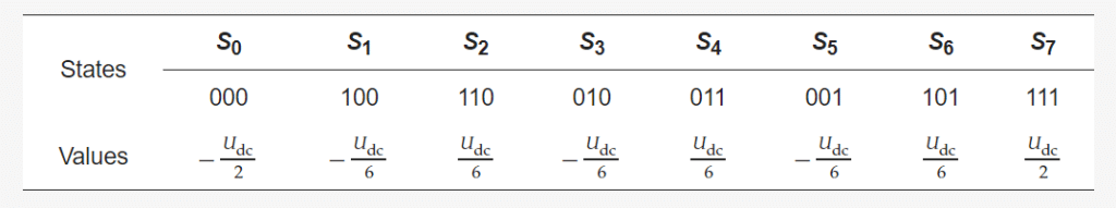
There are eight switch states for the inverter under the SVPWM strategy. The numbers 0 and 1 are utilized to denote the switch states of a bridge arm in an inverter. The state of 1 indicates that the upper device is closed while the lower device is open. The state of 0 indicates that the upper device is open while the lower device is closed. Consequently, the Vcm values of eight switch states are shown in Table 1, while the waveform of Vcm is shown in Figure 2.
In Figure 2, the Udc represents the dc bus voltage and the Ts represents the time of a switching cycle. The common-mode voltage Vcm is a four-level waveform under the SVPWM strategy. In this paper, the impact of switching frequency fs on the common-mode voltage Vcm and bearing voltage Vb is analyzed.

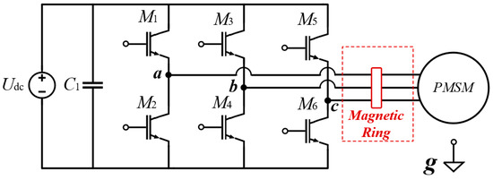
Figure 1. Schematic diagram of the motor drive system.
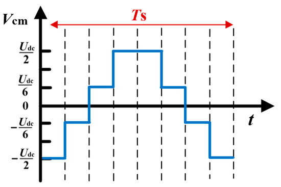
Figure 2. Waveform of common-mode voltage Vcm under SVPWM strategy.
Table 1. Common-mode voltage of the inverter under 8 switch states by using the SVPWM strategy.
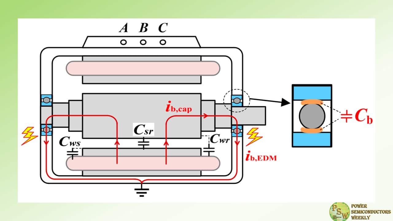
Under the excitation of high-frequency common-mode voltage, the impedance state of the motor exhibits a capacitive characteristic. As shown in Figure 3, Cws, Cwr, and Csr represent the parasitic capacitances of the winding to the stator core and to the rotor, and the stator core to the rotor, respectively. Cb represents the equivalent capacitance of the bearing grease oil film. These parasitic capacitances provide a low impedance coupling path for the high-frequency common-mode voltage.
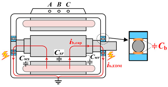
Figure 3. High-frequency parasitic capacitances inside the motor.
The generation process of bearing voltage and bearing current can be described by the equivalent circuit shown in Figure 4. The n point represents the neutral point in the star-connected motor. Vcm represents the common-mode voltage output from the inverter, and Vng represents the common-mode voltage at the motor neutral point. Lc and Rc are the equivalent common-mode inductance and resistance of the cable, respectively, and Lm and Rm are the equivalent common-mode inductance and resistance of the motor winding, respectively. The Rb is the equivalent resistance of the bearing, and Sb is the analog switch in the circuit.
After passing through the cable and the motor winding, Vcm generates Vng at the neutral point of the motor. Under the coupling effect of parasitic capacitances in the motor, a stable bearing voltage Vb is formed at both ends of the bearing lubricating grease film. At this time, the switch Sb in Figure 4 is open, and the change in bearing voltage regularly charges and discharges the oil film capacitance Cb to form the dv/dt capacitive bearing current ib,cap. The amplitude of ib,cap is small, and its influence on bearing electric corrosion is generally ignored.
When the Vb exceeds the voltage threshold of the lubricating grease oil film, the discharge phenomenon occurs. At the discharge moment, the oil film is no longer stable and the Vb drops to 0 V. At this time, the analog switch Sb in Figure 4 is closed, and Cb is shorted to simulate the breakdown and discharge process of the oil film.
The bearing current generated by the discharge is called EDM bearing current ib,EDM. The amplitude of ib,EDM is large, and the energy is released instantaneously. The heat released by multiple discharges could melt the rolling elements and raceways, which is the most direct cause of bearing electric corrosion. According to the above analysis, although the coupling paths of ib,cap and ib,EDM are the same, they do not occur simultaneously.
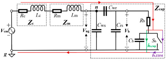
Figure 4. Common-mode equivalent circuit of a motor drive system.
2.2. Analytical Calculation Process
According to the common-mode equivalent circuit shown in Figure 4, the Vng is obtained as shown in Equation (2). Zc is the equivalent common-mode impedance of the cable, Zm the equivalent common-mode impedance of the motor winding, and Zcap is the common-mode impedance of parasitic capacitances inside the motor.

Ignoring the bearing resistance Rb, which is generally very small, the relationship between Vb and Vng is shown in Equation (3). KBVR is defined as the bearing partial pressure ratio, which is often used to roughly evaluate the electric corrosion degree of the bearing. When the bearing is in a stable rotating state, the bearing oil film thickness is stable. Cb is a constant value and KBVR can be considered as a constant.

According to Equations (2) and (3), the relationship between Vb and Vcm is shown in Equation (4). Vb is the result of the voltage division of Vcm through a common-mode equivalent circuit, and the waveform of Vb is consistent with those of Vcm and Vng, both of which are four-level waveforms. When the amplitude and frequency of Vcm are determined, Vb is decided by the common-mode impedances of the cable and motor, which in turn determines the magnitude of ib,EDM.

The accurate calculation of ib,EDM is very difficult, as it depends on the bearing voltage and the impedance of the bearing lubricating grease oil film. The thickness of bearing oil film highly depends on its speed, load, temperature, and the raceway surface roughness. During the rotation process, the lubricating grease oil film is uneven. When the bearing voltage exceeds the voltage threshold, the oil film would break down and discharge at its weakest position.
Therefore, the occurrence of the ib,EDM can be regarded as irregular, and some studies believe that it is random, following statistical probability. However, it should be noted that the occurrence probability of ib,EDM depends on the stable amplitude of the Vb and increases with the increase in Vb.
3. Analysis Model of a Common-Mode Equivalent Circuit for Bearing Voltage
3.1. Frequency Characteristics Analysis of Bearing Voltage
According to Equation (4), when Vcm is determined, the Vb and ib,EDM are mainly affected by the common-mode impedance of the cable and motor. Therefore, it is necessary to study the frequency characteristics of the common-mode impedance of the motor. The common-mode equivalent circuit in Figure 4 is simplified as shown in Figure 5, where Rcm, Lcm, and Ccm are the equivalent resistance, the inductance, and capacitance of the simplified common-mode circuit, respectively.
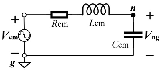
Figure 5. Simplified common-mode equivalent circuit of a motor drive system.
Based on the RLC series equivalent circuit in Figure 5, the variation law of Vng can be obtained by analyzing the voltage frequency characteristics of Ccm. According to Equation (3), the voltage frequency characteristics of Vb are consistent with Vng, so the amplitude–frequency characteristics of Vb can be obtained, as shown in Equation (5).
After the dc bus voltage of the inverter is determined, the Vcm amplitude is determined and the relationship between the Vb and frequency is obtained, as shown in Equation (6). The corresponding frequency–characteristic curve is shown in Figure 6. The P denotes the peak point, and the O denotes the resonant point of the curve in Figure 6. The ωP and ω0 are angular frequencies at points P and O, respectively.

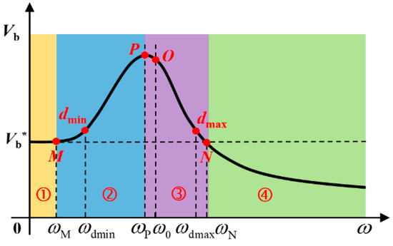
Figure 6. Frequency–characteristic curve of bearing voltage Vb.

In zone ① in Figure 6, the amplitude of Vb remains basically unchanged, and the Vb in this zone is defined as the reference bearing voltage Vb*. The point N is defined as the bearing voltage attenuation point, and the corresponding amplitude is also Vb*. The angular frequency ωN of point N is obtained as follows:

3.2. The Danger Zone and Safe Operating Zone of Bearing Electric Corrosion
As illustrated in Figure 6, the variation trend of Vb is associated with the system common-mode impedance parameters and switching frequency. With the increase in switching frequency, the amplitude of Vb shows a trend of first rising and then decreasing. The frequency–characteristic curve in Figure 6 is divided into four zones. The analysis of each zone is as follows:(1)
Zone ①: the frequency of common-mode excitation is before the ωM. With the increase in frequency, the amplitude of Vb increases slowly and the frequency dependence of Vb is low. This zone is defined as the bearing voltage stable zone. There is Vb ≈ Vb* in this region. The Vb is usually in this zone when the motor is driven by an IGBT inverter (typical switching frequency between 2 kHz and 8 kHz).(2)
Zone ②: the frequency of common-mode excitation is between ωM and ωP, and the amplitude of Vb increases significantly with the increase in frequency. This zone is defined as the bearing voltage growth zone. In this zone, there is always Vb > Vb*, and the Vb reaches its peak value at point P.(3)
Zone ③: the frequency of common-mode excitation is between ωP and ωN, and the amplitude of Vb decreases gradually with the increase in frequency. This zone is defined as the bearing voltage drop zone. In this zone, there is always Vb > Vb*, and Vb decreases to Vb* at point N. However, the amplitude of Vb is still large in this zone.(4)
Zone ④: when the frequency of common-mode excitation exceeds the ωN, Vb begins to decrease below Vb*, and the rate of decline gradually slows down with the increase in frequency. This zone is defined as the bearing voltage safety attenuation zone. In order to reduce the risk of bearing electric corrosion, it is hoped that the switching frequency of the inverter is located in this zone.
In order to better evaluate the impact of bearing voltage on bearing electric corrosion, the zone in Figure 6 where Vb ≥ 1.1 Vb* is defined as the bearing electric corrosion danger zone. According to Equation (6), the expressions of ωd_min and ωd_max of, respectively, the lower and upper frequency points in this zone are as follows:

In order to avoid the risk of bearing corrosion, the selection of switching frequency should try to avoid the danger zone between dmin and dmax in Figure 6. However, the selection of switching frequency is determined by many factors, such as efficiency, volume, power density, electromagnetic interference performance, etc. Therefore, the curve in Figure 6 can provide some references for the selection of the switching frequencies of SiC inverters.
Compared with other zones, zone ④ can obtain a smaller amplitude of Vb. Driven by a traditional IGBT inverter, Vb is often in region ①. However, the SiC device increases the switching frequency of the inverter, causing Vb to be located in zones ② or ③ with a large amplitude. This will increase the frequency and the harm degree of the EDM bearing current, causing serious bearing electric corrosion.
4. Experimental Measurement of Bearing Voltage and Bearing Current
4.1. Experimental Platform and Measurement Methods
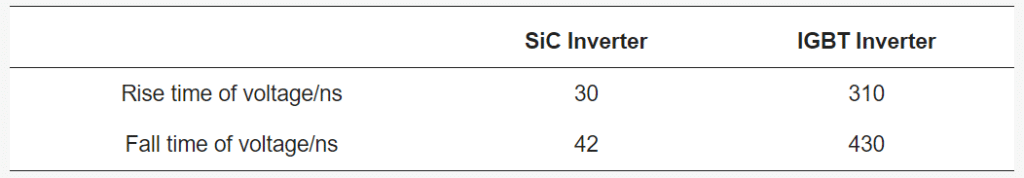
The experimental platform is established as shown in Figure 7. An embedded permanent magnet synchronous motor is adopted with 6007 deep groove ball bearings. The bearing manufacturer is SKF, a company headquartered in Gothenburg, Sweden. The rotor materials are permanent magnets and silicon steel sheets. The electrical parameters of the motor are shown in Table 2.
The motor is driven by an IGBT inverter or a SiC inverter, with rated powers of 10 kW, respectively. The IGBT inverter is purchased from KEB, a company headquartered in Barntrup, Germany. The SiC inverter is developed in-house in the laboratory. The bearing voltage is measured using a conductive brush. The bearing current is measured through an intrusive measurement method, which requires modification of the motor end cover.
An insulating layer is inserted between the bearing outer race and the motor end cover. Additionally, an external connection is established between the bearing outer race and the motor housing by using a short wire beside the motor for measuring bearing current.
The SVPWM strategy, 400 V bus voltage, and 0.5 m of unshielded cable are used in the experiment. The SiC transistor and the IGBT transistor used in this paper are the C2M0080120D and IGW40N120H3, respectively. The rise and fall times of output voltages for SiC inverter and IGBT inverter are provided in Table 3.
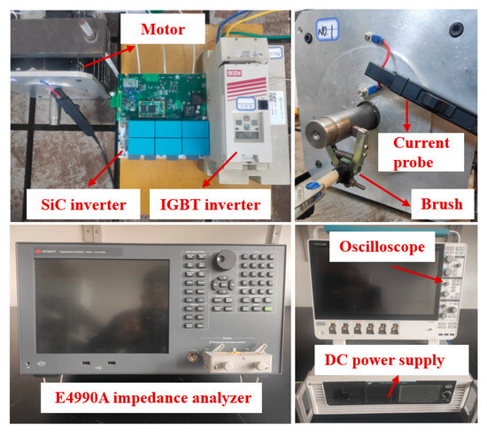
Figure 7. The experimental platform for the bearing voltage and current tests.
Table 2. The electrical parameters of the motor.
Table 3. The rise and fall times of output voltage for inverters.
For deep groove ball bearings, when the rotational speed is below approximately 300 r/min, the lubricating grease cannot completely envelop the ball, resulting in metal-to-metal contact between the ball and the inner and outer races. The bearing oil film is short-circuited, preventing the establishment of bearing voltage.
When the bearing speed is relatively high, the lubricating grease can generally form a stable oil film, allowing for the establishment of bearing voltage. Therefore, in order to ensure the stable establishment of bearing voltage, the motor speed used in the experiment is set at 1200 r/min with a modulation ratio of M = 0.4 in this paper.
4.2. Experimental Results under IGBT and SiC Inverters Drive
The experimental results of the motor neutral point voltage Vng, bearing voltage Vb, and bearing current were obtained using IGBT and SiC inverters, as shown in Figure 8. ib,de and ib,nde are, respectively, driven-end and non-driven-end bearing currents of the motor, and Tb is the temperature of the bearing outer race. In Figure 8, under the IGBT and SiC inverters’ drive, the stable amplitudes of Vb are approximately Vb_IGBT ≈ Vb_SiC = 6.3 V.
It indicates that the stable amplitude of the Vb is significantly influenced by the switching frequency but is only slightly affected by the switching speed. In Figure 8a, the maximum value of ib,EDM__IGBT is 55 mA, while in Figure 8b, the maximum value of ib,EDM__SiC is 57 mA, with the amplitudes being nearly equal. Different high-bandwidth current probes were employed for repeated testing, revealing that the 2 mA current difference is not measurement error but a real difference.
An explanation of this phenomenon is as follows: when the bearing rotates steadily, the lubricating grease film is uneven, and the raceway roughness is difficult to predict. Consequently, when breakdown discharge occurs in the oil film, the breakdown impedance is also different, which leads to slightly different amplitudes of ib,EDM under the same test conditions.
In the test conditions shown in Figure 8, both IGBT and SiC inverters were used, and a total of 30 sets of ib,EDM were captured in each case. The results show that although the bearing voltage amplitudes are equal, all captured amplitudes of ib,EDM fluctuate around 55 mA, with variations not exceeding 4 mA. This current fluctuation is considered normal and is not a result of measurement error.
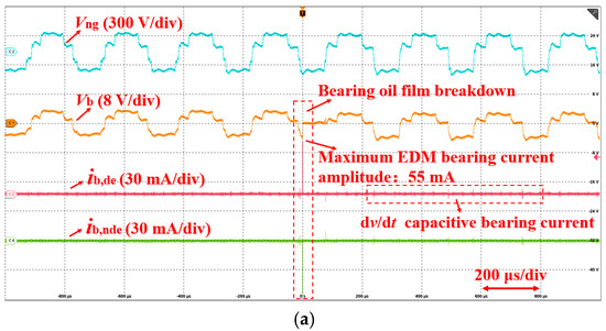
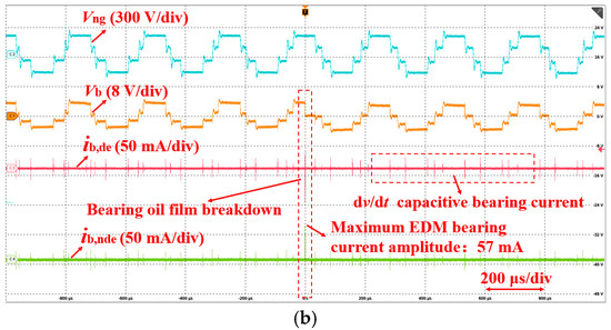
Figure 8. Measured waveforms of Vng, Vb, ib,de, and ib,nde (test conditions: SVPWM, Udc = 400 V, fs = 4 kHz, M = 0.4, Tb: 24~26 °C). (a) Under IGBT inverter drive; (b) under SiC inverter drive.
Since Vb_IGBT and Vb_SiC have similar amplitudes, the maximum amplitudes of ib,EDM__IGBT and ib,EDM__SiC are also approximately equal, indicating that the amplitude of Vb determines the energy of the ib,EDM.
Furthermore, from Figure 8, it can be observed that the capacitive bearing current ib,cap under the IGBT inverter is smaller than that in the SiC inverter, mainly due to the faster switching speed of the SiC inverter compared to the IGBT inverter.
According to Table 3, the switching speed of the SiC inverter is approximately one-tenth of that of the IGBT inverter. The amplitude of ib,cap is small, and the impact on bearing electric corrosion is also small. Under the IGBT inverter drive, ib,cap is generally neglected. However, under the SiC inverter drive, the impact of ib,cap on the bearing electric corrosion currently lacks relevant research conclusions.
4.3. Experimental Verification of Frequency Characteristics for Bearing Voltage and Current
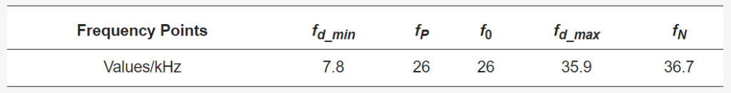
The experimental platform in Figure 7 is used for testing, and the measurement results of common-mode parameters of the motor and cable are obtained, as shown in Table 4. By substituting the parameters into Equations (7)–(11), the theoretical calculation results of points P, O, d_min, d_max, and N in Figure 6 are obtained. as shown in Table 5.
Table 4. The measured parameters of a common-mode equivalent circuit.

Table 5. Theoretical calculation results of frequency points for a Vb characteristic curve in the experimental system.
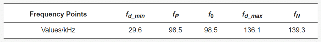
According to Table 5 and Figure 6, the analyses are as follows. When the switching frequency of the inverter used in the experiment exceeds 29.6 kHz, Vb begins to enter the danger zone in Figure 6. As the switching frequency increases, the amplitude of Vb increases significantly, reaching its maximum value at a frequency of 98.5 kHz. In the range from 98.5 kHz to 136.1 kHz, Vb begins to decrease, but it remains higher than the reference bearing voltage Vb*.
Therefore, when the switching frequency falls within the range from 29.6 kHz to 136.1 kHz, there is a significant risk of bearing electric corrosion. According to Figure 6, when the switching frequency exceeds 139.3 kHz, Vb starts to decrease below Vb*. In fact, constrained by electromagnetic interference and the control speed of the main controller, the switching frequency of the SiC inverter for the electric vehicle is generally lower than 100 kHz at present. Therefore, for the motor drive system adopted in the experiment, the Vb is located in zones ① and ② in Figure 6.
The theoretical calculation and experimental results of the Vb under different switching frequencies are obtained in Figure 9. The reference bearing voltage is Vb* = 6.3 V. When the switching frequency is less than 20 kHz, Vb increases slowly. In the range of 20 kHz–80 kHz, Vb increases quickly. Below 40 kHz, the theoretical calculations and experimental results are basically consistent. Above 40 kHz, with the increase in switching frequency, the error between the theoretical calculation and experimental results becomes more significant.
The analyses of error sources are as follows. Although the RLC lumped parameter equivalent circuit of the motor is simple, it is not accurate. In addition, there are measurement errors in the extraction of circuit parameters. Although there are errors at high frequencies, the overall variation trend of the bearing voltage is consistent with that of the frequency–characteristic curve depicted in Figure 6.
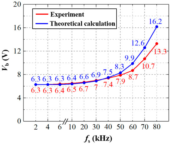
Figure 9. Variation trend of bearing voltage with switching frequency.
Figure 10 shows the number of ib,EDM occurrences (that is, the number of bearing oil film breakdown discharges) with the switching frequency per minute. The number of breakdown discharges was measured by taking the average value of multiple sample datasets. The results show that the increase in Vb could lead to the increased bearing breakdown discharges. The number of ib,EDM is approximately exponential with the rising switching frequency.
Based on Figure 10, the relationship between breakdown discharge times and switching frequency is obtained, as shown in Equation (12). Nd denotes the number of breakdown discharges. For the application in this paper, the values of the variables are A = 16.3, B = 8 × 10⁷, C = 137.9, D = 2, and E = 349.

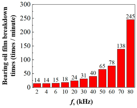
Figure 10. Variation trend of bearing oil film breakdown times with switching frequency.
The basic bearing voltage Vb*, especially at low switching frequency, already poses a significant threat to motor bearings. The increased switching frequency of the SiC inverter inevitably results in a further increase in bearing voltage. The dc bus voltage of the motor drive system is upgraded from 400 V to 800 V, which can double the bearing voltage. Therefore, with the increase in dc bus voltage and switching frequency, bearing voltage, and EDM bearing current are fatal to bearing damage, and effective suppression measures must be taken.
5. Design of Common-Mode Filter for Reducing Bearing Voltage and Current
The high switching frequency of the SiC inverter is advantageous for reducing the volume of the filter. Employing a common-mode filter to improve the frequency characteristics of a common-mode equivalent circuit and to suppress bearing voltage is an effective approach to mitigate bearing electric corrosion.
5.1. Theoretical Calculation and Experimental Verification for Common-Mode Filter
The actual operating frequency of the SiC inverter used in the experiment is 50 kHz. According to Table 5, the Vb of the experimental motor is located in zone ② in Figure 6, which is the danger zone. In order to greatly reduce the Vb, it is necessary to design a common-mode filter to ensure that Vb is located in zone ④, so as to reduce the risk of bearing electric corrosion. The common-mode equivalent circuit of the motor drive system with a common-mode filter is shown in Figure 11.
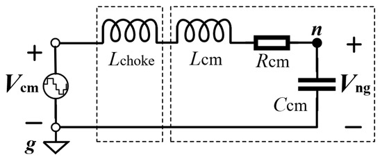
Figure 11. Common-mode equivalent circuit of the motor drive system with a common-mode filter.
In order to attenuate the Vb by at least half of the reference bearing voltage Vb*, according to Equation (6), the Equation (13) can be obtained:

Substituting the parameters in Table 4 into Equation (13), Lchoke ≥ 10.33 mH is obtained. The inductance of common-mode filter needs to be greater than 11 mH. In order to achieve Vb ≤ 0.5Vb*, the actual designed common-mode filter has a certain margin, and the final inductance value is 13 mH.
There is an error in the actual and theoretical design of the inductance value, which mainly arises from the following three aspects: the presence of other harmonic components in the common-mode excitation Vcm, inherent errors in the lumped parameter equivalent circuit, measurement errors in the extraction of common-mode parameters, and parasitic parameters in the filter. The above factors cause the error between the theoretical and actual inductance values in this paper.
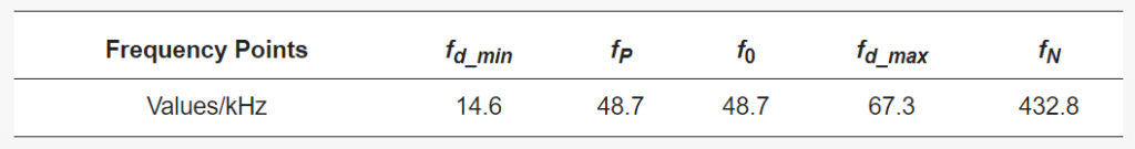
According to the equivalent circuit model shown in Figure 11, when the inductance of the common-mode filter changes, the frequency characteristics of the motor drive system also change accordingly. Correspondingly, the curve of Vb also changes with frequency in Figure 6. According to Equations (7)–(11), the theoretical calculation results of each frequency point at the curve in Figure 6 are shown in Table 6 by using a 13 mH common-mode filter.
Table 6. Theoretical calculation results of frequency points for the Vb characteristic curve in the experimental system (Lchoke = 13 mH).
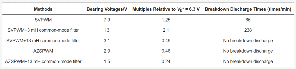
The experimental waveforms are shown in Figure 12. In Figure 12a, the amplitude of Vb is 7.9 V without a common-mode filter, and the maximum amplitude of ib,EDM is 120 mA. Vb is located in zone ② of Figure 6. In Figure 12b, after using a common-mode filter, the measured amplitude of Vb is 3.1 V, and Vb is located in zone ④ of Figure 6, which is reduced to 0.49 times of the reference value Vb* = 6.3 V. By using a common-mode filter, significant attenuation of Vb is obtained, and no discharge of oil film occurs during the experiment.
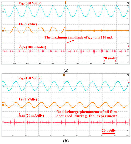
Figure 12. Measured waveforms of Vng, Vb, and ib (test conditions: SVPWM, Udc = 400 V, fs = 50 kHz, M = 0.4, Tb: 24~26 °C). (a) Without common-mode filter; (b) with a 13 mH common-mode filter.
5.2. Negative Effects Caused by Improper Design of a Common-Mode Filter
In order to suppress electromagnetic interference in practical applications, a magnetic ring is often used at the output end of inverter, as shown in the red box in Figure 1. The magnetic ring can be equivalent to a common-mode filter with a single turn coil, which has a small inductance. The Vb is usually located in zone ① of Figure 6 when using an IGBT inverter with a low switching frequency. According to Figure 6 and Equation (6), the amplitude of Vb is basically not increased when the common-mode magnetic ring is installed at the output end of inverter.
Therefore, the magnetic ring is used to suppress electromagnetic interference while minimizing the negative impact on Vb. However, when using a SiC inverter with a high switching frequency, Vb is located in zone ② in Figure 6. If the magnetic ring is still installed at the output end of the inverter to suppress electromagnetic interference, according to Equation (6), Vb would increase significantly, thereby increasing the risk of bearing electric corrosion.
To illustrate the above issue, a common-mode filter with a small inductance of 3 mH is used for the analysis. The frequency points of the curve in Figure 6 are recalculated and the results are shown in Table 7. According to Figure 6 and Table 7, if the inverter still adopts the switching frequency fs = 50 kHz, which is close to the resonant frequency of the system in Table 7, the amplitude of Vb is large. As a result, the bearings will face a significant risk of electric corrosion.
Table 7. Theoretical calculation results of frequency points for the Vb characteristic curve in the experimental system (Lchoke = 3 mH).
Still using the same testing conditions as in Figure 12, the experimental results are shown in Figure 13. The measured amplitude of Vb reaches 13 V, which is 65% higher than that (7.9 V) in Figure 12a. This significantly increases the breakdown times and discharge energy of the bearing oil film. The number of breakdown discharges per minute measured is as high as 238 times, and the maximum EDM bearing current is 250 mA, which is approximately twice that (120 mA) shown in Figure 12a.
Based on the theoretical and experimental results above, the switching frequency fs = 50 kHz in the experiment is close to the peak point frequency in Figure 6, inevitably leading to excessive bearing voltage and serious bearing corrosion.
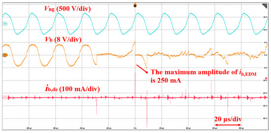
Figure 13. Measured waveforms of Vng, Vb, and ib (test conditions: SVPWM, Udc = 400 V, fs = 50 kHz, M = 0.4, Tb: 24~26 °C, Lchoke = 3 mH).
In summary, for the SiC motor drive system, the design of a common-mode filter or magnetic ring needs to consider the suppression effects on both electromagnetic interference and bearing voltage. It is essential to refer to the design methods proposed in Section 3. Otherwise, improper filter design may exacerbate the bearing electric corrosion.
6. The Suppression Method for Bearing Current in a Motor Drive System with a High-Voltage SiC Inverter
In order to relieve the design pressure of the bearing in the motor drive system with a high voltage and high frequency, the AZSPWM strategy is adopted to weaken the common-mode voltage of the inverter from the source. Then, a common-mode filter is adopted for the output end of the inverter to further reduce the bearing voltage, reducing the discharge times and the discharge energy of the bearing oil film.
6.1. The AZSPWM Strategy
With the SVPWM strategy, the maximum value of the common-mode voltage is Udc/2 when using the zero vector. A non-zero vector modulation strategy can be used to reduce the common-mode voltage amplitude by canceling the zero vector.
Considering the switching loss, modulation ratio, and harmonics, the AZSPWM strategy is adopted in this paper. The comparison of the vector synthesis for SVPWM and AZSPWM-1 in sector I is shown in Figure 14. The idea of AZSPWM-1 is to replace the zero vector by using two non-zero vectors in opposite directions acting at the same time, so that the amplitude of the common-mode voltage is suppressed to Udc/6.
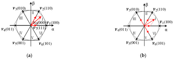
Figure 14. Comparison of vector syntheses for different modulation strategies (taking sector I as an example). (a) SVPWM; (b) AZSPWM-1.
The AZSPWM strategy is divided into three types: AZSPWM-1, AZSPWM-2, and AZSPWM-3. The suppression effect on the common-mode voltage is the same for all three modulation strategies. For AZSPWM-2 and AZSPWM-3, the two bridge arms of the inverter need to operate simultaneously, leading to increased losses. Therefore, the AZSPWM-1 strategy is adopted. The AZSPWM-1 strategy may increase current harmonics, but the high switching frequency of the SiC inverter can reduce these current harmonics, compensating for this drawback.
With the AZSPWM-1 strategy, the common-mode voltage waveform is shown in Figure 15. The amplitudes are different in the even sector and odd sector, but the maximum value is Udc/6, which is one-third of the maximum value Udc/2 under the SVPWM strategy.
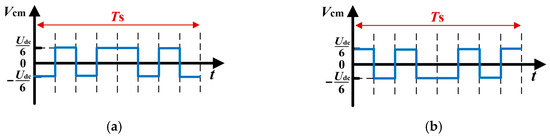
Figure 15. Diagram of common-mode voltage waveform under AZSPWM-1 strategy. (a) Even sector; (b) odd sector.
6.2. The Suppression Effect of Bearing Voltage and Bearing Current
Still using the same testing conditions as Figure 12, the experimental results are shown in Figure 16. In Figure 16a, the AZSPWM-1 strategy is adopted and the amplitude of Vb is reduced to 2.9 V, which is 63% lower than that of 7.9 V driven by SVPWM in Figure 12a. In Figure 16b, the combination of AZSPWM-1 and the 13 mH common-mode filter is adopted. The amplitude of Vb is reduced to 1.5 V and the Vb is greatly attenuated. During the experiment, no discharge phenomena occurred.
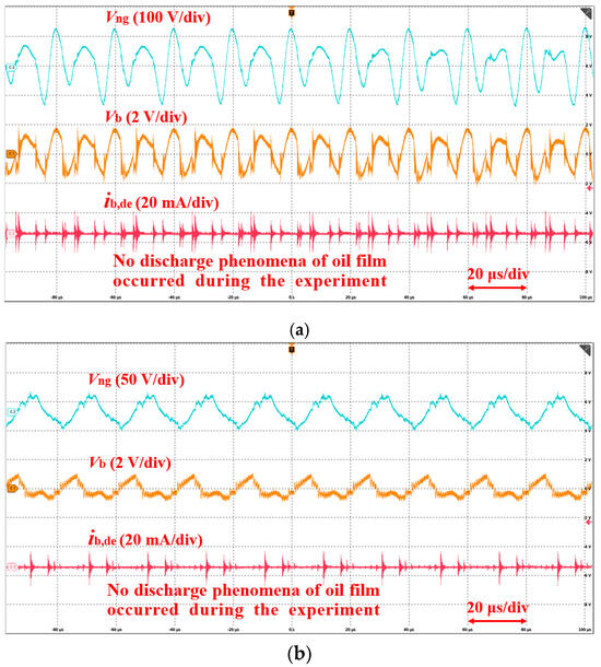
Figure 16. Measured waveforms of Vng, Vb, and ib (test conditions: SiC inverter, AZSPWM-1, Udc = 400 V, fs = 50 kHz, M = 0.4, Tb: 24~26 °C). (a) Without common-mode filter; (b) with a 13 mH common-mode filter.
The comparison results of bearing voltage amplitudes and breakdown discharge times are shown in Table 8 under different suppression methods. The combination of AZSPWM-1 and the common-mode filter achieves the best suppression effect, reducing the bearing voltage to 1.5 V. It effectively suppresses the EDM bearing current and is highly suitable for a motor drive system with a high voltage and high frequency.
Table 8. Comparison results of bearing voltage and discharge times under different suppression methods.
7. Conclusions
This paper investigates the characteristics and suppression methods of bearing voltage and EDM bearing current under SiC inverter drive. By establishing the common-mode equivalent circuit of the motor drive system, the frequency characteristics of bearing voltage are revealed. The suppression method is proposed, which is suitable for a motor drive system with a high voltage and high frequency. Through theoretical analysis and experimental validation, the following conclusions are drawn.
Compared to a traditional IGBT inverter, the SiC inverter with a high switching frequency increases the amplitude of bearing voltage, exacerbating the risk of bearing electric corrosion. The selection of switching frequency must consider the impact on the bearing voltage and the EDM bearing current.
For motor drive systems with a SiC inverter, the design of the common-mode filter or magnetic ring needs to consider the influence on bearing voltage and current. Otherwise, negative effects may occur, aggravating bearing electric corrosion. The proposed design method of common-mode filter can improve the frequency characteristics of bearing voltage, attenuating the bearing voltage to half of the reference bearing voltage and keeping it in the safe operating zone.
The AZSPWM-1 strategy can attenuate the bearing voltage to around half of the reference bearing voltage. When combining AZSPWM-1 and a common-mode filter, the bearing voltage is reduced to around one-fourth of the reference bearing voltage, achieving the best suppression effect. This method effectively reduces the breakdown times of lubricating grease oil film, which is suitable for motor drives with a high voltage and high frequency in electric vehicles.
Authors
Mingliang Yang, Yuan Cheng, Bochao Du, Yukuan Li, Sibo Wang, Shumei Cui.
Original – MDPI
-

Navitas Semiconductor announced its participation in the upcoming Power Electronics International conference on April 16th– 17th 2024, in Brussels, Belgium.
Grid reliability is a key factor in a $1.3 trillion power semiconductor opportunity as Navitas’ technologies accelerate the transition from fossil fuels to renewable energies. Navitas will introduce the latest GaNFast™ and GeneSiC™ products to the European audience, including new Gen-3 Fast SiC for high-power and higher-speed performance, plus GaNSafe™ – the world’s most protected GaN power devices.
Navitas will present the following on April 17th:
- “3.3 kV SiC MOSFETs Accelerate Grid-Connected Energy Storage,” Dr. Ranbir Singh, EVP GeneSiC
Synopsis: The grid supplies energy from generators and delivers it to customers via transmission and distribution (T&D) networks. In the U.S., the use of electricity storage to support and optimize T&D has been limited due to high storage costs and limited design and operational experience. Recent improvements in storage and power technologies, however, coupled with changes in the marketplace, herald an era of expanding opportunity for electricity storage. SiC inverters will revolutionize electricity delivery, renewable energy integration, and energy storage. It is well-recognized that silicon-based semiconductors have inherent limitations that reduce their suitability for utility-scale applications.
- “Bi-directional circuits open up new opportunities in off-grid applications,” Alfred Hesener, Senior Director Industrial and Consumer Applications
Synopsis: Bi-directional circuits are critical to effectively smooth the supply/demand variation in renewable energy applications. In the past, they were expensive to make and complex to implement in power electronics applications. Wide bandgap GaN power ICs with integrated drive and advanced circuit functions deliver easy-to-use, reliable, high power density, and functionality for power factor correction circuits, solar inverters, and solid-state circuit breakers.
Original – Navitas Semiconductor
-

EPC Space announced a distribution agreement with Avnet, a global distributor of electronic components and services. Avnet will be a global distributor for EPC Space’s line of radiation hardened (Rad Hard) GaN power devices qualified for satellite and high-reliability applications.
EPC Space offers a family of Rad Hard power GaN devices that includes discrete transistors, Integrated Circuits (ICs), and Modules that offer significant performance advantages over competitive silicon-based space level power devices. EPC Space’s GaN technology devices are smaller, have lower resistance, and have superior switching performance compared to silicon-based components and solutions.
Critical spaceborne applications that benefit from the performance improvements that EPC Space devices offer include satellite’s DC-DC converters, reaction and momentum wheels, solar array drive assembly, micro-pumps for propulsion systems, and more.
“Partnering with Avnet, a global leader in distribution solutions, allows EPC Space to offer timely and reliable service to customers seeking high reliability GaN power solutions,” said Bel Lazar, EPC Space’s CEO.
Original – EPC Space
-

Wolfspeed, Inc. hosted Senator Thom Tillis (R-NC) and other local officials, community partners, and employees at a ceremony to celebrate the topping out of construction at the $5 billion John Palmour Manufacturing Center for Silicon Carbide. Located in Chatham County, North Carolina, the JP will produce 200mm silicon carbide wafers, significantly expanding Wolfspeed’s materials capacity, and meet the demand for next generation semiconductors critical to the energy transition and AI.
“We are excited to mark this critical milestone alongside our hard-working team, loyal customers, community partners, and ardent supporters like Senator Thom Tillis,” said Wolfspeed President and CEO, Gregg Lowe.
“This facility is a testament to Wolfspeed’s commitment to our local community and domestic workforce, furthering our position as the global leader in silicon carbide production. The JP will help maintain America’s lead in energy innovation, and unlock significant benefits for our local community by growing the state’s economy by more than $17.5 billion over the next two decades and creating 1,800 good-paying jobs by 2030.”
“Wolfspeed’s $5 billion investment in Chatham County is another example of why North Carolina is the best state in the country to do business,” said Senator Tillis. “I was proud to vote in favor of the CHIPS and Science Act, which provides critical support for domestic semiconductor manufacturing, and I applaud Wolfspeed’s commitment to developing technology here in North Carolina that supports our national security and economic interests.”
The JP represents a total investment of $5 billion, complemented by public and private support, to help accelerate the transition from silicon to silicon carbide and ramp up supply of this material recently deemed as critical to the energy transition by the U.S. Department of Energy. By the end of 2024, phase one of construction is expected to be completed on the 445-acre site.
The ramp of the JP will support recently signed customer agreements with Renesas, Infineon, and additional companies, while driving meaningful progress towards Wolfspeed’s long-term growth strategy. The JP will primarily produce 200mm silicon carbide wafers, which are 1.7x larger than 150mm wafers, translating to more efficient wafers and ultimately, lower costs. The JP underpins Wolfspeed’s vision of accelerating the adoption of silicon carbide semiconductors across a wide array of end-markets and unlocking a new era of energy efficiency.
Wolfspeed currently produces more than 60% of the world’s silicon carbide materials at its Durham, N.C. headquarters, and is engaged in a $6.5 billion capacity expansion effort to dramatically increase production.
Original – Wolfspeed
-
Abstract
In this paper, a novel asymmetric trench SiC MOSFET with a Poly-Si/SiC heterojunction diode (HJD-ATMOS) is designed to improve its reverse conduction characteristics and switching performance. This structure features an integrated heterojunction diode, which improves body diode characteristics without affecting device static characteristics.
The heterojunction diode acts as a freewheeling diode during reverse conduction, reducing the cut-in voltage (Vcut-in) to a lower level than conventional asymmetric trench SiC MOSFET (C-ATMOS), while maintaining a similar breakdown voltage. Meanwhile, the split gate structure reduces gate-to-drain charge (Qgd). Through TCAD simulation, the HJD-ATMOS decreases Vcut-in by 53.04% compared to the C-ATMOS. Both Qgd and switching loss are reduced, with a decrease of 31.91% in Qgd and 40.29% in switching loss.
1. Introduction
The wide bandgap semiconductor properties of silicon carbide (SiC) make it a promising candidate for the development of future power switching devices. This is primarily due to SiC possessing properties such as a strong breakdown field, high physical and chemical stability, high thermal conductivity, and high electron saturation velocity.
SiC devices can operate in harsh environments due to their wide band gap of 3.25 eV and high thermal conductivity of 5 W/(cm·K). The SiC MOSFET is the most significant SiC power switching device due to its lack of trail current. This reduces switching loss and radiator volume, improving system power density.
SiC MOSFETs commonly make use of parasitic body-PN diodes as freewheeling diodes (FWD) in power inverter and converter systems. However, parasitic body-PN diodes in SiC MOSFETs are not ideal for use as freewheeling diodes. The reasons for this are as follows: Stacking faults (SFs) in SiC devices may cause reliability issues and increase conduction loss.
Although recent papers concerning the measured degradation of SiC MOSFETs show a high level of current threshold (about 5× the nominal current or more than 1000 A/cm2) for the starting of bipolar degradation, bipolar degradation effects can still occur in SiC MOSFETs under large cyclic pulse current densities. This will limit the application of SiC MOSFET devices in key areas, such as the surge current that flows through a diode during the start-up of a power converter, which can be more than ten times its rated current.
Furthermore, the body diode’s Vcut-in voltage (~2.7 V) is much higher than that of its silicon counterparts due to SiC’s wide bandgap. To overcome the drawbacks of parasitic body-PN diodes, numerous approaches have been devised to deactivate them. One approach is to integrate SiC MOSFETs with Schottky barrier diodes (SBDs). However, the use of external diodes not only introduces parasitic inductance, limiting switching frequency, but also consumes additional area in the package. And Schottky contacts suffer from a significant increase in reverse leakage current at high temperatures.
Furthermore, SiC MOSFETs with low-barrier and heterojunction diodes are available. Heterojunction diodes formed between polysilicon and SiC are attractive. Shenoy and Baliga, and Yamagami et al. presented studies on heterojunction diodes using P-Poly-Si and n-6H-SiC, and Poly-Si and 4H-SiC, respectively.
Both studies demonstrated low-forward-voltage Schottky-like characteristics. Ni et al. proposed a trench SiC MOSFET integrating polysilicon/SiC HJD, exhibiting excellent freewheeling diode (FWD) performance in both the first and third quadrants. The HJD’s unipolar behavior, similar to that of a Schottky diode, effectively suppresses the turn-on of the problematic body diode, mitigating the aging degradation observed in conventional SiC MOSFETs.
Additionally, HJDs reduce reverse recovery voltage and losses, enhancing long-term operational reliability. Furthermore, HJD integration eliminates the need for a separate SBD, leading to a smaller chip area, simpler packaging, and reduced overall system cost. This also minimizes parasitic inductance arising from additional components.
A novel asymmetric trench SiC MOSFET with a heterojunction diode at the right of the gate trench is proposed and simulated in this paper. The structure includes a trench gate with split-gate electrodes and a thicker P-Poly-Si layer, resulting in reduced gate charge and improved switching performance. To suppress the depletion layer, an n-type doped current spreading layer (N-CSL) is formed under the entire P-well region.
To maintain the breakdown voltage (BV) of the device structure while maintaining transfer and output characteristics similar to those of C-ATMOS, the depth of the P-well on the right side is not changed. The N-channel (Nch) is positioned below the P-Poly-Si and in contact with the CSL. The integrated HJD structure of the proposed device eliminates the requirement for an anti-parallel SiC SBD during reverse conduction. The HJD turns on at a low source–drain voltage (Vsd), thus eliminating bipolar degradation by inactivating the body diode. The split gate results in a decrease in gate charge, leading to a reduction in switching losses in the HJD-ATMOS without affecting other characteristics.
2. Device Structure and Mechanism
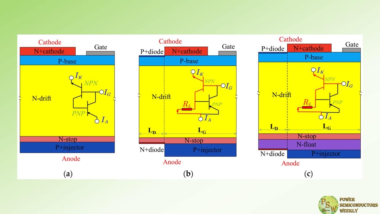
The schematic cross section of HJD-ATMOS and C-ATMOS is shown in Figure 1. Similar to C-ATMOS, the device forms an inversion layer channel in the first quadrant to facilitate electron conduction. The N-CSL layer on the N-drift region reduces the on-resistance. Deep P-wells are used to reduce the electric field stress in the gate oxide at the trench bottom and corner.
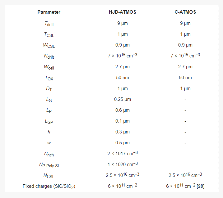
The primary distinction is the body diode structure. The Nch region under the P-Poly-Si provides a low-barrier path for electrons. Meanwhile, the HJD-ATMOS has a split gate and HJD structure on the right of the gate oxide layer. The split gate structure uses only a portion of the trench space for the gate electrode, while the other part is thicker P-Poly-Si that forms a portion of the HJD structure. The HJD-TMOS facilitates low-voltage conduction by allowing electrons to cross the lower heterojunction barrier in the third quadrant. The structure of Nch and N-channel doping concentration (Nnch) will be further discussed based on this optimization in this paper. Device specifications are presented in Table 1.
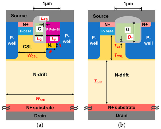
Figure 1. Schematic cross section of (a) HJD-ATMOS and (b) C-ATMOS.
Table 1. Main parameters used in the simulation.
Sentaurus TCAD simulations are used to analyze the performances of the HJD-ATMOS and the C-ATMOS, considering doping and temperature-dependent Shockley–Read–Hall and Auger recombination, doping-dependent transport, impact ionization, band narrowing, high-field velocity saturation, and mobility degradation, as well as fixed charges at the SiC/SiO2 interface for closer simulation results to experimental data.
The energy band diagram of the P-Poly-Si/N-SiC heterojunction at thermal equilibrium is shown in Figure 2b. The energy band diagram at thermal equilibrium along the A-A’ cut-line is shown in Figure 2a. The heterojunction has a conduction energy gap of 0.46 eV and a valence barrier energy gap of 1.78 eV. The electron barrier height ΦBN is determined by the Fermi level energy Ef and the conduction band peak energy Ec, which is about 1.39 eV.
Figure 2c shows the simulated carrier density at the heterojunction interface under forward bias at the rated voltage. Electrons are injected from N-SiC to P-poly, but there are few holes from P-poly to N-SiC due to the high hole barrier. Therefore, the HJD exhibits unipolar action, similar to the SBD.
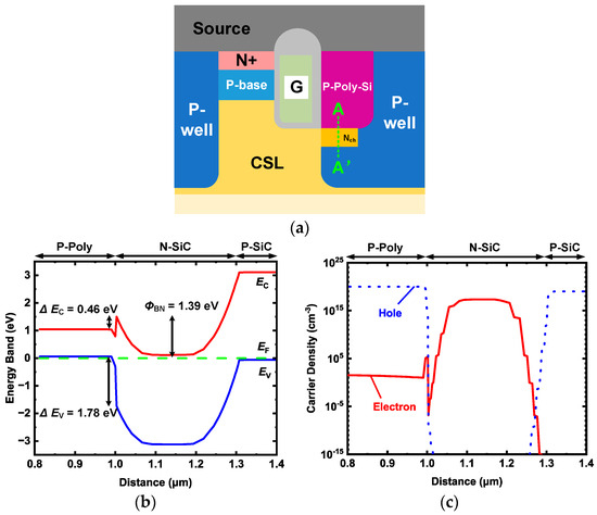
Figure 2. (a) Schematic cross section of HJD-ATMOS; (b) energy band diagram at thermal equilibrium along the A-A’ cut-line; (c) carrier density of the HJD when forward biased at rated voltage.
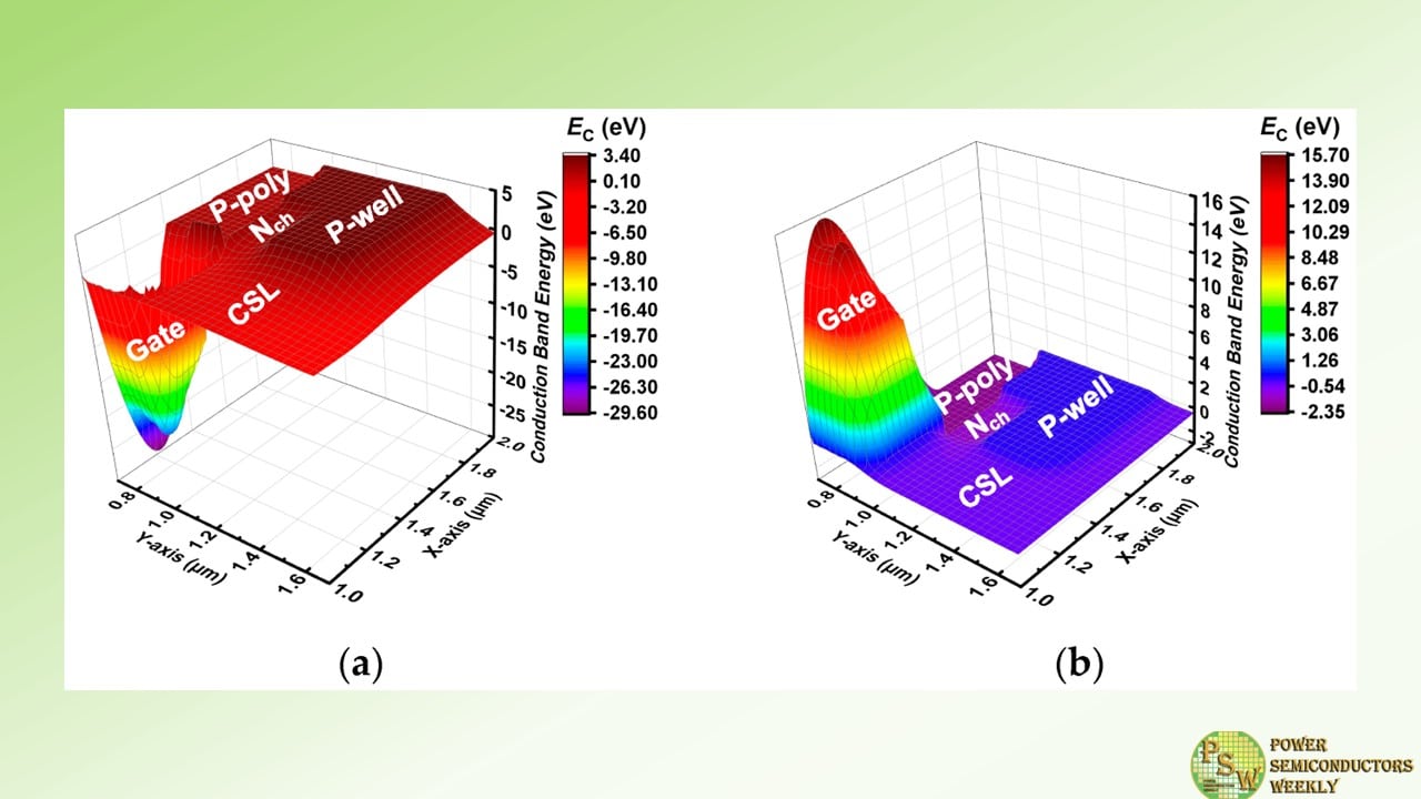
We also constructed a 3D band diagram of the device to better observe the working state of the device. Figure 3a shows the 3-D conduction band energy distribution of the device at Vds = 10 V and Vgs = 15 V. The band energy of Nch is higher than that of N-CSL, which prevents electron current from flowing to P-poly and enables the device to work normally like C-ATMOS.
Figure 3b shows the distribution of the devices when Vds = −5 V and Vgs = −5 V. The band energy of Nch is lower than that of N-CSL, resulting in electron current flowing from N-CSL to P-poly and preventing the turn-on of parasitic body-PN diodes.
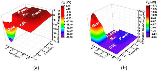
Figure 3. Three-dimensional conduction band energy distribution between P-poly, gate, Nch, N-CSL, and P-well (a) when conduction is forward and (b) when conduction is reverse.
Figure 4 shows the distribution of the total current density, hole current density, and electron current density of the device. From the total current density distribution, it can be seen that the current does not flow from P-Poly-Si to P-well. But a high current density is also noted at the gate corner of P-Poly-Si, which should be noted in use. From the hole current density distribution, it can be seen that holes do not enter N-drift.
This is due to the difference in the band gap between SiC and polysilicon. Since the energy barrier height between the SiC and polysilicon junctions in the valence band is very large, in the HJD-ATMOS, electron current can move toward the source while hole current cannot move toward the drain. The device can operate normally at electron current densities of 10 A/cm2 and 500 A/cm2.
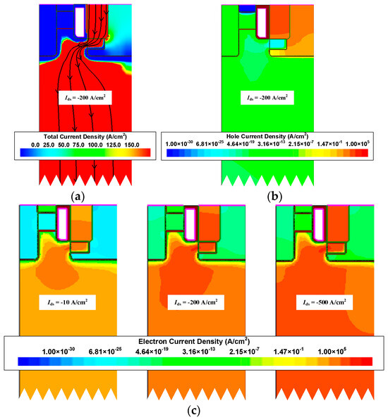
Figure 4. (a) Total current density distribution, (b) hole current density distribution, and (c) electron current density distribution at low and high current in the reverse conduction.
Figure 5 shows the I–V curves of HJD-ATMOS and C-ATMOS in forward and reverse conduction at room temperature. The steeper slope of the I–V curve of HJD-ATMOS in the first quadrant indicates that its specific on-resistance (Ron,sp) is lower than that of C-ATMOS. This is because the presence of Nch in HJD-ATMOS results in a smaller depletion region of P-well on N-CSL, leading to a wider current conduction region.
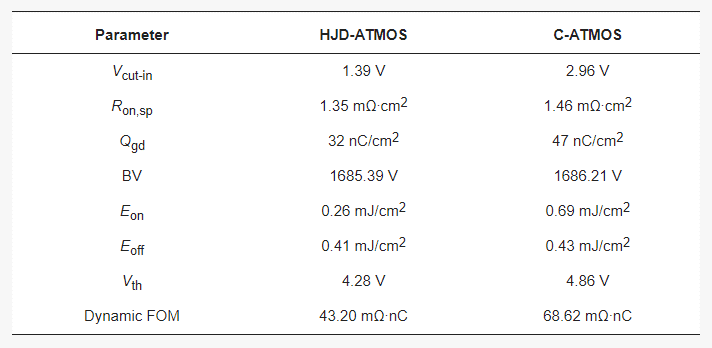
According to the calculations, at Vgs = 15 V and Ids = 200 A/cm2, the Ron,sp values for HJD-ATMOS and C-ATMOS are 1.35 mΩ∙cm2 and 1.46 mΩ∙cm2, respectively. In the third quadrant, at Ids= −10 A/cm2, HJD-TMOS exhibits a significantly lower Vcut-in of only 1.39 V compared to the PN diode of C-TMOS. As a result, HJD-ATMOS is capable of reducing switching losses.
The rated operating current of the device in the third quadrant is generally Ids = −200 A/cm2. This means that the proposed HJD-ATMOS has a clear advantage over C-ATMOS in that it can start working at a lower voltage. The hole density distribution diagram in Figure 5 for Ids = −200 A/cm2 shows that the integrated HJD effectively suppresses minority carrier injection, reducing bipolar degradation.
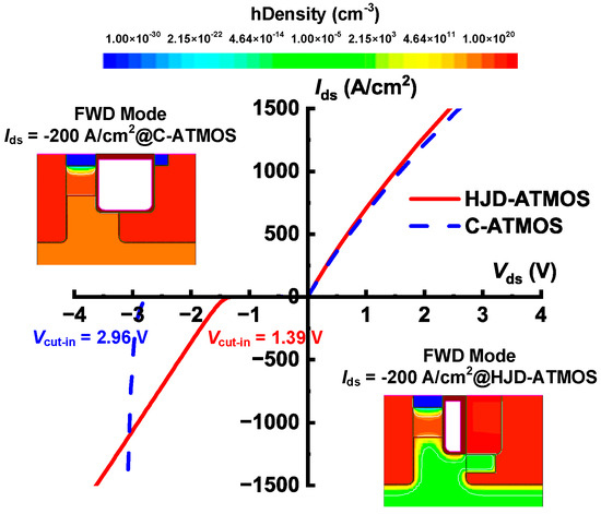
Figure 5. First and third quadrant characteristics of HJD-ATMOS and C-ATMOS.
In Figure 6, the local magnification shows that the HJD-ATMOS is affected by current spikes due to leakage. The figure demonstrates the change in breakdown voltage as a function of h and w when Nnch is, respectively, 2 × 1017 cm−3 and 2.5 × 1017 cm−3. It can be observed that when Nnch is 2.5 × 1017 cm−3, with h at 0.25 μm and w at 0.5 μm, the spike in the current is large, indicating the occurrence of leakage. When Nnch is 2.5 × 1017 cm−3, increasing h to 0.30 μm and w to 0.4 μm also results in leakage.
However, when Nnch is 2.0 × 1017 cm−3 and h increases to 0.3 μm, the device does not exhibit leakage, demonstrating that variations in Nnch have a significant impact on device performance. As shown in Figure 7, Vcut-in varies significantly with h. The minimum point of Vcut-in is 1.31 V at Nnch = 2 × 1017 cm−3, which is lower compared to its value of 1.71 V at Nnch = 2.5 × 1017 cm−3 and h = 0.2 μm.
This point represents the critical condition for the device not exhibiting leakage when Nnch = 2.5 × 1017 cm−3. After h is greater than 0.25 μm, the variation in Vcut-in with h tends to be flat, and if the value of h is larger, the protective effect of P-well on the gate oxide will also be weakened, and it will also increase the difficulty of process manufacturing.
As can be seen from Figure 8, when the device Vds is 0 V, Nnch is 2.5 × 1017 cm−3, and h is 0.25 μm, the HJD-ATMOS has more leakage than the device with Nnch is 2.0 × 1017 cm−3 and h is 0.30 μm. The darker regions in the current density plot for the HJD-ATMOS with Nnch at 2.5 × 1017 cm−3 and h at 0.25 μm are larger than those with Nnch at 2.0 × 1017 cm−3 and h at 0.30 μm, indicating higher leakage currents. This also confirms the hypothesis that the breakdown voltage spike is caused by heterojunction leakage. So the results indicate that Nnch = 2 × 1017 cm−3, h = 0.3 μm, and w = 0.5 μm are the optimal values.
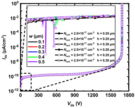
Figure 6. The breakdown voltage varies with h, w, and Nnch, when Nnch is 2.0 × 1017 cm−3 and 2.5 × 1017 cm−3, h is 0.20 μm, 0.25 μm and 0.30 μm, and w is 0.1 μm to 0.5 μm, respectively.
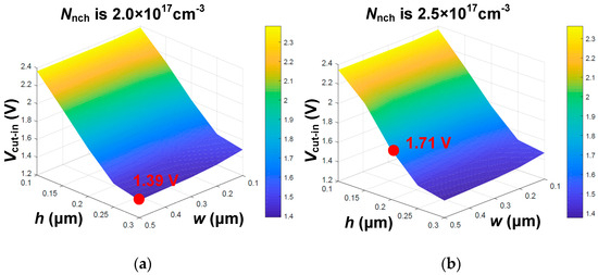
Figure 7. Vcut-in varies with h, w, and Nnch, when Nnch is (a) 2.0 × 1017 cm−3, and (b) 2.5 × 1017 cm−3.
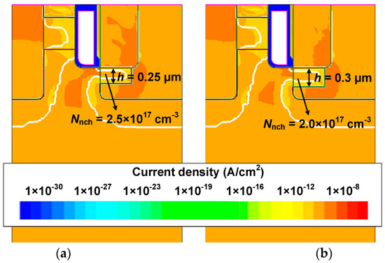
Figure 8. Current density distribution when (a) Nnch is 2.5 × 1017 cm−3, h is 0.25 μm, and (b) Nnch is 2.0 × 1017 cm−3, h is 0.30 μm at Vds = 0 V.
3. Simulation Results and Discussion
Figure 9 shows the capacitances of HJD-ATMOS and C-ATMOS. Gate voltage was fixed at 0 V, a 1 MHz AC signal was applied, and drain voltage was swept from 0 to 1000 V. HJD-ATMOS has lower gate-to-source capacitance (Cgs) than C-ATMOS due to the smaller contact area with the source caused by the split gate structure. HJD-ATMOS’s gate-to-drain capacitance (Cgd) does not decrease.
This is because the P-well blocks the right side of the gate of C-ATMOS, performing a similar function as the split gate. Therefore, it can be observed that the Ciss (Cgs + Cgd) of the HJD-ATMOS with split gates is also smaller than that of the C-ATMOS.
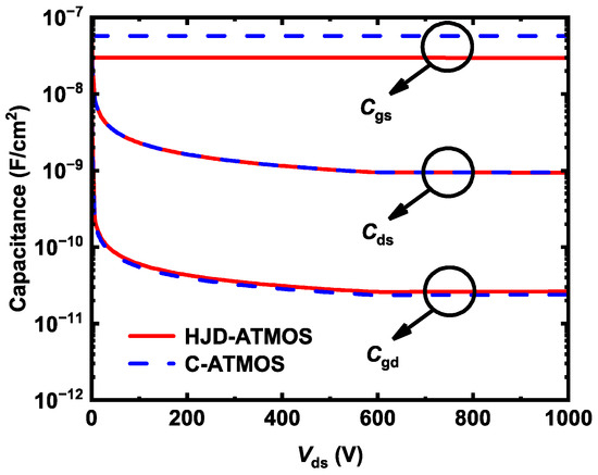
Figure 9. The device capacitance of HJD-ATMOS and C-ATMOS.
Gate-to-drain charge (Qgd) is critical for power device switching speed in device applications. Figure 10 shows a test circuit to simulate HJD-ATMOS and C-ATMOS gate charges during turn-on. The miller plateau height of HJD-ATMOS is less than that of C-ATMOS, indicating that the threshold voltage of HJD-ATMOS is smaller than that of C-ATMOS.
Because the gate charge is proportional to the gate capacitance, the HJD-ATMOS has a lower gate charge (Qg) and Qgd compared with the C-ATMOS. The Miller platform in HJD-ATMOS is shorter because of the reduced gate area. The Qgd values for HJD-ATMOS and C-ATMOS are 32 nC/cm2 and 47 nC/cm2, respectively. Qgd of HJD-ATMOS decreased by 31.91% compared to C-ATMOS. Reduced Qgd leads to a smaller high-frequency figure of merit in HJD-ATMOS.
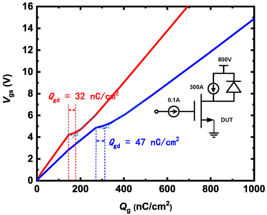
Figure 10. The gate charge characteristics of HJD-ATMOS and C-ATMOS.
Figure 11 shows the electric field distribution at the breakdown of HJD-ATMOS and C-ATMOS. The electric field at the gate oxide of HJD-ATMOS is smaller than that of C-ATMOS. This is because the presence of the Nch introduces a portion of the electric field into this region, which alleviates the electric field that the gate oxide withstands.
Although increasing the electric field at the heterojunction raises leakage current risk, it is a trade-off for improved reverse conduction performance. Figure 12 shows the blocking characteristics of the HJD-ATMOS and the C-ATMOS at room temperature and high temperature. At room temperature, the data are represented by solid lines, whereas at elevated temperatures, they are depicted by dashed lines. HJD-ATMOS and C-ATMOS have similar breakdown voltages at room temperature. But the leakage current of the HJD-ATMOS increases at high temperature due to the increased thermal energy of the charge carriers.
The generation of leakage currents, as demonstrated and discussed in Figure 6 and Figure 8, arises due to leakage occurring at the heterojunction, where higher Nnch and greater values of thickness h both contribute to this effect. By improving the semiconductor material growth process, reducing defects and traps, and enhancing the material quality and interface integrity, it is possible to mitigate non-ideal scattering and trap effects experienced by charge carriers at the heterojunction interface, thus suppressing the leakage current.
While the HJD-ATMOS structure does indeed experience leakage under temperature influence, this leakage is within acceptable limits, with the level of leakage current being 1 × 10⁻⁵ μA/cm2.
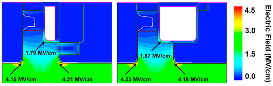
Figure 11. Electric field distribution for the HJD-ATMOS and the C-ATMOS at BV.
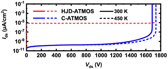
Figure 12. Blocking characteristics of the HJD-ATMOS and the C-ATMOS.
Figure 13 shows a double pulse test circuit for investigating switching characteristics. This is a common circuit configuration employed in device testing. Stray inductance is 10 nH, and load inductance is 80 μH. The gate voltage source (Vg) is turned on from −5 V to 15 V at t = 16 µs and turned off from 15 V to 0 V at t = 11 µs.
Figure 14 shows the switching waveforms of devices. The switching speed of the HJD-ATMOS is faster than that of the C-ATMOS with an external SBD diode, which results in a smaller switching loss. Figure 15 compares the switching losses between the two devices. In HJD-ATMOS, the turn-on loss (Eon) is 0.26 mJ/cm2, and the turn-off loss (Eoff) is 0.41 mJ/cm2, which demonstrate a reduction of 62.32% and 4.65%, respectively, compared to C-ATMOS.
The total switch loss of HJD-ATMOS is reduced by 40.29% compared to C-ATMOS. This is due to the smaller Qgd compared with the C-ATMOS. Reduced switching losses in power electronic devices are instrumental in improving operational longevity and reliability. As losses during switching are directly proportional to heat generation, a significant decrease in these losses curtails thermal build-up, mitigating the risk of device overheating and extending its operational life.
This reduction also sustains lower junction temperatures, crucial for preventing material degradation in high-power-density applications where maintaining low operating temperatures is vital for ensuring long-term stability and reliability. Furthermore, minimizing switching losses allows power converters and similar equipment to function efficiently at elevated frequencies without sacrificing efficiency, empowering designers to develop compact, lightweight systems while consistently meeting reliability standards.
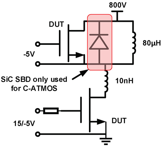
Figure 13. A circuit for simulating switching with a double pulsed test.
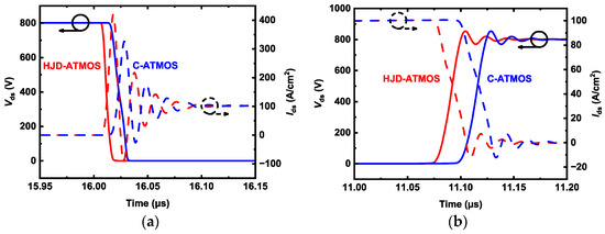
Figure 14. The switching characteristics of HJD-ATMOS and C-ATMOS, including the (a) turn-on process and (b) turn-off process.
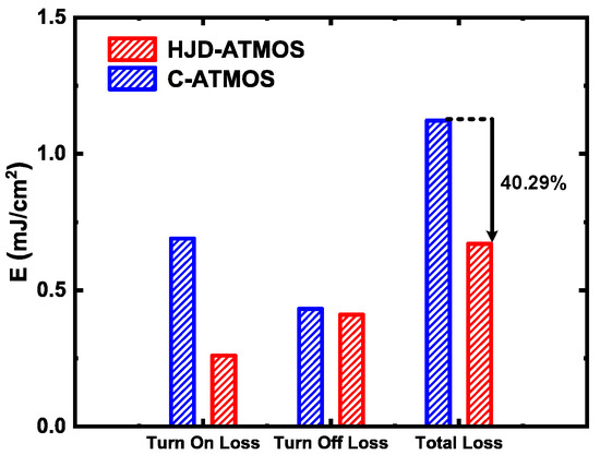
Figure 15. Switching loss comparison of IJ-ATMOS and C-ATMOS.
The majority of the process steps for HJD-ATMOS, including epitaxial growth, N+ source and P-well implantation, trench etching, P-base implantation, isolation oxidation, gate oxidation, polysilicon gate deposition, and metallization, are fully compatible with the manufacturing processes of C-ATMOS.
The N-channel region is formed by ion implantation at the bottom of the trench after trench etching. The split gate is formed by etching after trench oxidation, resulting in a thin layer of oxide between the gate and the P-Poly-Si. The gate-P-Poly-Si trench isolation layer is formed by thermal oxidation, and the trench oxide layer is fully etched and filled with P-Poly-Si.
Table 2 compares the HJD-ATMOS and the C-ATMOS in terms of their main characteristics. Dynamic FOM indicates the value of Ron,sp × Qgd. The HJD-ATMOS performs better due to the integrated HJD structure.
Table 2. Device characteristics comparison.
4. Conclusions
This paper proposes a novel asymmetric trench SiC MOSFET with a heterojunction diode. The performance of HJD-ATMOS and C-ATMOS is compared in detail. It can be observed that HJD-ATMOS demonstrates superior third-quadrant performance with a lower Vcut-in because of the integrated HJD. Compared with C-ATMOS, the Qgd of HJD-ATMOS has decreased by 31.91%. This is because the split gate design further reduces the total gate charge, which reduces the switching loss of the HJD-ATMOS device without affecting other key characteristics.
As a result, HJD-ATMOS eliminates bipolar degradation and reduces the turn-on loss from 0.69 mJ/cm2 in C-ATMOS to 0.26 mJ/cm2. With its advantageous features, HJD-ATMOS is a strong contender for power electronic applications.
Authors
Yiren Yu, Zijun Cheng, Yi Hu, Ruiyi Lv, Shengdong Hu.
Original – MDPI
-

In the paper “Milliseconds Power Cycling (PCmsec) Driving Bipolar Degradation in Silicon Carbide Power Devices”, Sibasish Laha from Fraunhofer IISB and his co-authors Jürgen Leib, Andreas Schletz, Martin Maerz, Christian Liguda, Firas Faisal and Davood Momeni describe an innovative approach to silicon carbide (SiC) power cycling.
Until now, bipolar degradation (BD) tests have not been sufficiently differentiated in the investigation of failure and fault mechanisms for SiC power devices. SiC power products may experience voltage degradation which stems from the stacking faults (SFs) growth, commonly known as BD. To properly evaluate the BD impact on the electric performance of devices, it is important to distinguish it from other stress-related degradation such as power metal or interconnection.
This aspect has not yet been addressed, although the BD mechanism is well understood. The paper outlines a methodology by modifying the power cycling test (PCsec) to PCmsec in order to systematically investigate the effect of BD while controlling the impact of thermal degradation. This method enables a thorough evaluation of the distinct influences of both degradation contributors.
The complete paper will soon be available in the CIPS proceedings. Until then, feel free to download the paper presentation on event page.
There you can also find all our contributions to CIPS 2024:- Modified Approach for the Rainflow Counting Analysis of Temperature Load Signals in Power Electronics Modules – Oral presentation by S. Letz; Co-authors: D. Zhao, J. Leib, B. Eckardt, M. März
- Milliseconds Power Cycling (PCmsec) Driving Bipolar Degradation in Silicon Carbide Power Devices – Oral presentation by S. Laha; Co-authors: D. Momeni, J. Leib, A. Schletz, M. März, C. Liguda, F. Faisal
- Challenges of Junction Temperature Calibration of SiC MOSFETs for Power Cycling – a Dynamic Approach – Poster by J. Breuer, F. Dresel, A. Schletz, J. Klier, J. Leib, M. März, B. Eckardt
- Wide Bandwidth PCB Rogowski Coil Current Sensor with Droop Suppression and DC Restoration for In-Situ Inverter Measurements – Poster by S. Quergfelder, J. Sax, T. Heckel, B. Eckardt, M. März
Original – Fraunhofer IISB
-

Innoscience Technology firmly denounces the accusations made by Infineon Technologies Austria AG in a recent patent infringement lawsuit against three Innoscience entities. Infineon filed this lawsuit in a U.S. district court in California on March 13, 2024, and asserted a single U.S. patent.
Innoscience denies Infineon’s allegations of patent infringement as well as the validity of the Infineon patent. Innoscience will vigorously defend itself and is confident that it will prevail. Infineon’s intention with this litigation is also in question, as it has asserted a patent that has significant defects. Particularly, even a cursory review of Infineon’s patent portfolio reveals that the alleged “invention” of the asserted patent was already disclosed in Infineon’s own earlier prior art patents, raising concerns that it may have committed fraud on the United States Patent and Trademark Office, for not making proper disclosures during the prosecution of the asserted defective patent.
In addition, contrary to Infineon’s wrong characterization that the claims of the asserted defective patent “cover core aspects of GaN power semiconductors,” the lawsuit only concerns a small fraction of Innoscience’s packaged high-voltage (650V-700V) GaN transistors and does not affect the vast majority of its other products (including unpackaged transistors and wafers, low-voltage transistors, and certain packaged transistors).
Therefore, the lawsuit should have little to no effect on Innoscience’s current ability to make, use, sell, offer to sell, or import into the United States its products for customers. Innoscience respects others’ valid IP rights and is also dedicated to developing its own IP portfolio. Despite being an eight-year old company, Innoscience has filed more than 800 patent applications globally. Innoscience’s R&D team boasts 500+ technical experts across the world.
Through continuing innovation, Innoscience has produced GaN devices to power a diverse range of products, from power delivery chargers to data centers and smartphones, showcasing its ability to align with evolving application demands and adapt to diverse customer specifications.
Moreover, Innoscience has always sought a cooperative and mutually beneficial approach to develop the global GaN industry, even among others in the same industry. Innoscience intends to prevail in this pending lawsuit and is determined to remain a trusted and reliable partner for its customers and contribute to their success by offering top-notch and versatile products and solutions based on Innoscience’s home-grown, superior technologies.
Original – Innoscience Technology
-
Abstract
In this study, a novel integrated 4H-SiC reverse-conducting gate turn-off thyristor (GTO) featuring an N-type floating (NF) structure is proposed. The proposed NF-structured 4H-SiC GTO outperforms conventional reverse-conducting GTOs in forward conduction, effectively eliminating the snapback phenomenon.
This is achieved by increasing lateral resistance above the P-injector and modifying the electron current path during early turn-on. NF structures with a doping concentration of 2 × 1014 cm−3 and thicknesses exceeding 4 μm have been indicated to successfully eliminate the snapback phenomenon. Moreover, the anode-shorted structure enhances the GTO’s breakdown voltage and concurrently reduces turn-off losses by 85% at low current densities.
1. Introduction
In recent years, advancements in power distribution and energy transmission applications, including smart grids, ultra-high voltage power transportation, and pulse power technology, have heightened the demand for high-voltage power devices. Typically, conventional silicon (Si) power devices can withstand voltages up to 8 kV. Beyond this limit, complex arrangements of converters or devices become necessary, especially in ultra-high voltage contexts.
This necessity has shifted the focus towards wide bandgap (WBG) semiconductors, particularly 4H-SiC, renowned for their superior material characteristics. 4H-SiC is increasingly favored for fabricating ultra-high voltage and high-frequency power devices because of its exceptional properties: a bandgap three times wider than that of silicon, a critical breakdown electrical field ten times higher, and an electron saturation velocity surpassing silicon by an order of magnitude.
In recent years, significant strides have been made in refining the SiC epitaxial growth process, marked by noteworthy advancements in enhancing charge carrier lifetimes and reducing bulk- and interface-trap densities. These improvements have been instrumental in achieving substantial progress in the development of high-voltage SiC devices.
Wolfspeed (formerly known as Cree Inc., Durham, NC, USA) have announced their development of SiC MOSFETs with impressive blocking voltages of 10 kV and 15 kV. Concurrently, there has been a technological breakthrough in bipolar devices rated above 20 kV, achieving PIN diodes with blocking voltages ranging from 7 to 39 kV, further pushing the boundaries in high-voltage device engineering. In addition, 10 kV SBD and JBS diodes have also been produced.
In 2015, the voltage and current capabilities of SiC IGBTs saw a significant enhancement, reaching 27.5 kV/20 A. In 2013, Cree Inc. advanced the SiC p-GTO’s performance to 20 kV, followed by the development of a 15 kV SiC n-GTO in 2019. Furthermore, in 2017, a SiC Emitter Turn-Off Thyristor (ETO) p-ETO with a blocking voltage of 22 kV was reported, exemplifying continued advancements in SiC device technology.
Additionally, researchers are focusing on the stacking technology of SiC-based power devices for ultra-high voltage applications. In the study ‘Theoretical and Experimental Study of 22 kV SiC Emitter Turn-OFF (ETO) Thyristor’, an assessment of the forward current handling capacities of 15 kV SiC GTO (p-type), IGBT, and MOSFET at temperatures of 25 °C and 125 °C was conducted.
This analysis clearly indicates that the SiC GTO outperforms in terms of managing higher currents with the least forward voltage drop, marking it a key player for the next generation of ultra-high power devices. In the research documented in ‘Evaluation of Ultrahigh-Voltage 4H-SiC Gate Turn-OFF Thyristors and Insulated-Gate Bipolar Transistors for High-Power Applications’, simulation models were employed to validate that within a range of 20–50 kV, SiC GTOs exhibit a voltage drop of 3.4–7.8 V at a current density of 20 A/cm2 at room temperature, whereas IGBTs display a voltage drop between 4.2 and 10 V under similar conditions.
The underlying reason for this enhanced performance of SiC GTO, from the viewpoint of semiconductor current conduction, is its capability for bidirectional carrier injection and pronounced conductivity modulation in the drift region. Therefore, the SiC GTO is emerging as a highly viable option for ultra-high voltage power applications.
However, the intense conductivity modulation effect leads to an increased turn-off time, subsequently slowing down the switching speed. In the case of GTO devices, turn-off losses constitute a major part of the overall switching losses, prompting considerable efforts in recent years to minimize these losses. To enhance GTO performance, various structures such as Integrated Gate-Commuted Thyristors (IGCT), Emitter Turn-Off (ETO) Thyristors, and Reverse-Conducting GTOs (RC-GTO) have been proposed.
The Reverse-Conducting GTO (RC-GTO) introduces an innovative design that combines a diode with a GTO at the cellular level. This integrated architecture functions as a high-voltage forward switch and, when reversed, operates as a continuous current diode. Traditional GTOs, lacking reverse conduction capability, necessitate parallel connection with a reverse diode.
Thus, compared to conventional GTOs, RC-GTOs offer enhanced power density, streamlined system design, and improved thermal cycling of the chip. However, like RC-IGBTs, conventional RC-GTOs suffer from an undesirable snapback effect, which hinders the device from fully turning on. In this study, a novel integrated SiC Reverse-Conducting GTO (RC-GTO) structure featuring an N-type floating region (NF-RC-GTO) is presented. This design effectively suppresses and eliminates the snapback phenomenon, minimally impacting the primary performance. Additionally, it features low turn-off loss at low current densities.
2. Device Structure and Mechanism
Figure 1a–c illustrate the simulation structures and equivalent circuit diagrams of the GTO, conventional RC-GTO (con-RC-GTO), and NF-RC-GTO, respectively. The SiC GTO is comprised of five layers: p-n-n-p-n, which functionally resemble two back-to-back PNP and NPN bipolar junction transistors (BJTs). The currents in these two BJTs are interdependent, and the device activates when the sum of the common-base current gains, denoted as αPNP and αPNP for the PNP and NPN BJTs, respectively, exceeds 1.
Compared to a standard GTO, both the conventional RC-GTO (con-RC-GTO) and the NF-RC-GTO feature an anode-shortened structure and a cathode-shortened structure, functioning as a reverse diode. In the equivalent circuit of a SiC RC-GTO, the additional connection to the N-drift region is modeled as a resistor (RL) placed parallel between the base and emitter terminals of the inherent PNP bipolar transistor (BJT). RL is nonlinear, primarily determined by the shape and doping concentration of the N-stop (and for NF-RC-GTO, also the N-float) regions.
During the initial phase of forward-conduction mode, the RC-GTO operates akin to an NPN BJT. This continues until the conduction current is sufficient to cause the voltage drop across RL to exceed 2.7 V, which is approximately the turn-on threshold voltage of a conventionally doped SiC PN junction at room temperature, fully activating the emitter-base junction of the inherent PNP transistor.
Once activated, the inherent PNP transistor contributes to conductivity modulation in the N-drift region, leading to a significant decrease in the resistance between the cathode and anode of the device. Subsequently, the RC-GTO transitions to operate as a conventional GTO. This shift from NPN BJT to GTO operation is marked by a voltage jump and an exponential increase in anode current, a process known as the snapback phenomenon.
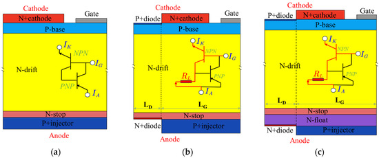
Figure 1. Structures and equivalent circuit diagrams of the devices under study. (a) GTO; (b) conventional RC-GTO; (c) NF-RC-GTO.
To mitigate the snapback effect, the NF-RC-GTO incorporates an additional N-float layer with a lower doping concentration (such as 2 × 1014 cm−3). This layer boosts the lateral resistance above the P-injector, directing current flow through areas of higher resistance and enabling the emitter-base junction of the intrinsic PNP bipolar transistor to activate at much lower currents.
It is important to note the symmetrical relation of the cathode-shortened region to the gate structure in the NF-RC-GTO, which simplifies the formation of the cathode-shortened structure, especially when compared to traditional SiC-nGTO fabrication processes.
The performance of the various structures was simulated using Synopsys Sentaurus Technology Computer-Aided Design software, which computes fundamental physical partial differential equations and physical models, such as the Poisson equation and diffusion and transport equations, to facilitate the simulation of the structure and electrical characteristics of semiconductor devices.
Please note, all subsequent results are derived from simulation experiments. The basic physical models utilized in the TCAD simulations encompass impact ionization, incomplete ionization, Shockley–Read–Hall and Auger recombination, doping concentration-dependent carrier lifetime, and electric field and doping concentration-dependent carrier mobility.
The average lifetimes of carriers are defined as 2.5 µs for electrons and 0.5 µs for holes, which align with values commonly found in commercially available epitaxial layer structures. The standard parameters for the 13 kV SiC NF-RC-GTO, SiC con-RC-GTO, and con-GTO are compiled and presented in Table 1.
Table 1. Device parameters for simulations.
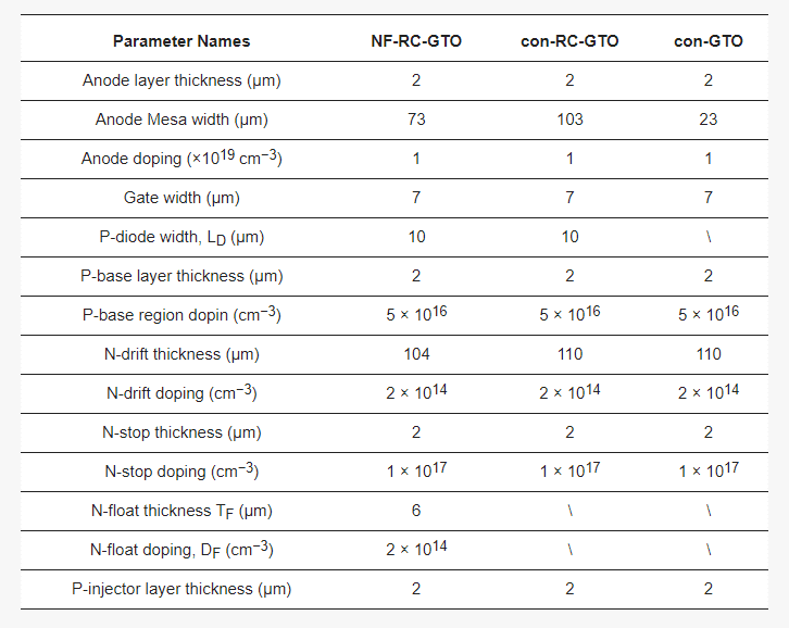
Figure 2 displays the current–voltage (I–V) characteristics for the GTO, con-RC-GTO, and NF-RC-GTO. In terms of forward turn-on performance, the conventional GTO exhibits optimal characteristics with a smooth transition, notably absent of any snapback effect.
For the RC-GTO variants, prior to the turn-on of the anode P/N diode, the devices exhibit behavior akin to an NPN BJT, a result of the additional electron excess provided by the N+ diode region. Specifically, in the case of the con-RC-GTO, a broader LG dimension diminishes the snapback effect. As LG widens from 110 μm to 120 μm, there is a notable reduction in the snapback voltage from 6.11 V down to 4.83 V.
Conversely, the NF-RC-GTO sees the complete elimination of the snapback effect with a reduced LG width of just 80 μm, affirming the effectiveness of the N-float structure in mitigating this issue. Furthermore, the forward conduction voltage drop (measured at a current density of 100 A/cm2) is comparable to that of the con-RC-GTO.
It is important to consider that an oversized LG dimension may lead to an uneven distribution of current within the device. This imbalance can result in thermal concentration issues, and additionally, it has the potential to diminish the available space for the reverse PN diode structure.
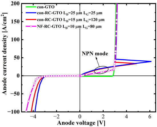
Figure 2. The current–voltage (I–V) characteristics of the GTO, con-RC-GTO, and NF-RC-GTO.
Figure 3 illustrates the initial paths of electron and hole currents during the conduction mode. Specifically, Figure 3a depicts the flow of electron current into the P-collector, bypassing the N-stop layer and entering the N-float layer in the NF-RC-IGBT under unipolar mode. This dual-layer structure effectively channels the current flow through the N-float region, significantly increasing the path resistance.
The current flow lines shown in Figure 3b confirm this. The voltage across the P-injector and N-float junction, distant from the N region, reaches at least 2.7 V at the earliest stage. Subsequently, the P-injector at this juncture begins to inject holes, facilitating conductivity modulation. Consequently, the device transitions into operating as a GTO.
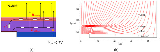
Figure 3. (a) Current flow path; (b) current flow lines at the Anode side of the NF-RC-GTO in low current density mode.
The simple snapback model used for Figure 3a can be described as follows:

For the NF-RC-GTO, the N-float layer is pivotal in directing the current flow through areas of high resistance. This underscores the necessity for meticulous design of both the doping concentration and the geometry of the N-float region to more effectively suppress the snapback phenomenon.
3. Results
Figure 4 displays the characteristic curves of the forward off-state breakdown voltage. The breakdown voltages for the NF-RC-GTO, con-RC-GTO, and con-GTO are 15,303 V, 15,992 V, and 13,730 V, respectively. Both the NF-RC-GTO and con-RC-GTO, featuring an anode-short structure, exhibit higher breakdown voltages compared to the conventional GTO. Notably, the NF-RC-GTO shows an 11.4% improvement over the con-GTO.
This enhanced performance is attributed to the anode-short circuit structure, which allows leakage current from the reverse-biased junction to directly exit through the short-circuited anode. This mechanism also prevents hole injection at the P+ injector region, reducing the common-base current gain of the anode PNP BJT, thereby increasing the forward breakdown voltage. The slightly lower breakdown voltage of the NF-RC-GTO, compared to the con-RC-GTO, is due to the NF structure, which results in a shorter ndrift structure (104 µm).
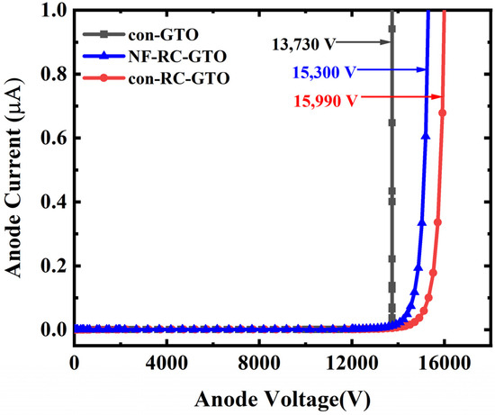
Figure 4. BV curves of the con-GTO, con-RC-GTO, and NF-RC-GTO, respectively. The gate voltage is zero.
Figure 5 provides insight into the effect of doping concentration in the float region on the forward and reverse performance of NF-RC-GTOs, which are characterized by a consistent thickness of 4 μm and an LG length of 80 μm. The figure reveals that as the doping concentration decreases, the snapback voltage also reduces, and the snapback phenomenon completely vanishes at a doping concentration of 2 × 1014 cm−3.
This trend can be attributed to the increased lateral resistance above the P-injector resulting from the lower doping concentration, consequently leading to a reduced snapback voltage. Additionally, during the initial turn-on phase, the current in the NPN mode diminishes as the lateral resistance increases. It is also observed that with a higher doping concentration, the current handling capability slightly decreases. This is due to an increase in the compound current within the NF region, which negatively affects the hole injection efficiency in the anode region.
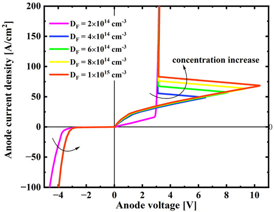
Figure 5. Forward and reverse conduction characteristics of the NF-RC-GTO with different N-float doping concentration (DF).
Figure 6 delineates the impact of the N-float structure’s thickness on the forward and reverse performance of NF-RC-GTOs. These devices share a consistent doping concentration and LG dimension for the N-float structure, at 2 × 1014 cm−3 and 80 μm, respectively.
The figure indicates that the snapback voltage decreases with an increase in the thickness of the N-float structure. Notably, the snapback phenomenon is eliminated when the thickness exceeds 3 μm. This effect can be attributed to the thicker N-float structure reducing the direct flow of NPN mode current through the N-stop region to the anode-short structure during the initial turn-on phase.
As a result, a higher proportion of electrons flow through the N-float region to the anode-short structure, facilitating earlier hole injection in the anode P-injector/N-float region. Furthermore, Figure 6 also reveals that variations in the thickness of the N-float structure within a certain range do not significantly affect the NF-RC-GTO’s forward and reverse high-current handling capability.
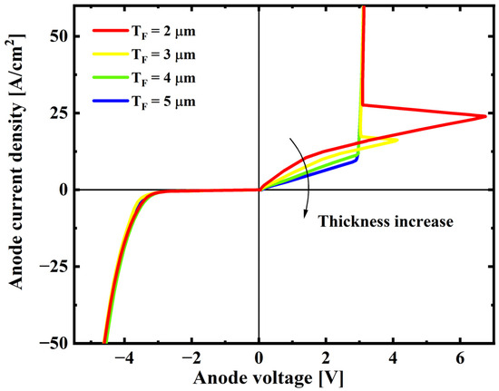
Figure 6. Forward and reverse conduction characteristics of the NF-RC-GTO with different thickness of N-float structure (TF).
The transient characteristics of the newly proposed NF-RC-GTO, with varying widths of the Anode-shortened structure (LD), are analyzed during the turn-off processes. A double pulse test (DPT) circuit is employed for evaluating the dynamic switching performance.
The DPT setup includes a high-voltage DC power supply of 8000 V, a gate resistor of 5 Ω, a clamped inductive load of 5 mH, and a gate signal of 15 V/−100 V to provide sufficient gate trigger current. At t = 0, the current in the inductor begins to increase from 0 at a rate of 1.6 A/µs. At t = 15 µs, the gate signal VG = 15 V is applied to trigger the turn-on of all GTOs, which lasts for 15 µs. At t = 30 µs, the gate signal switches to VG = −100 V to initiate the turn-off process.
Figure 7 displays the voltage and current waveforms of devices during the turn-off process, showcasing variations with different LD values in the DPT discharge circuits. The results show that the NF-RC-GTO surpasses the conventional GTO in the turn-off test.
This superior performance is attributed to the Anode-shortened structures of the NF-RC-GTO, which expedite the extraction of stored carriers, thus significantly accelerating the shutdown process. Additionally, for the NF-RC-GTO, a wider LD correlates with a shorter turn-off time. However, the turn-off time does not continue to decrease when LD exceeds 10 μm, as the carrier extraction path is already sufficiently wide at this point.
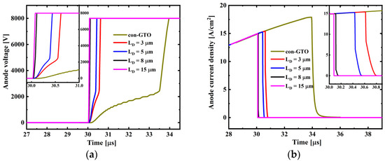
Figure 7. (a) Voltage and (b) current waveforms during turn-off process.
For the NF-RC-GTO, the device initially operates in BJT mode until the current reaches a level high enough to trigger the switch to GTO mode operation. This implies that the conductance modulation effect in the drift region is not fully activated, indicating that the concentration of injected non-equilibrium carriers in this region is lower than in conventional GTOs. Consequently, fewer carriers need to be extracted from the drift region during the turn-off process, resulting in a significantly reduced turn-off time compared to standard GTO devices.
Figure 8 displays the distribution of electron and hole concentrations in the drift region along the device’s vertical direction during normal turn-on at 15 A/cm2. The carrier concentration distribution for the NF-RC-GTO is observed to be in the range of 1 × 1016 cm−3, markedly lower than that of the con-GTO. This reduced carrier concentration is the fundamental reason behind the NF-RC-GTO’s rapid turn-off speed.
Therefore, the NF-RC-GTO possesses the potential for faster turn-off when the current to be switched off is not excessively high. The transition point from BJT to GTO mode in the device is indicated by a sudden increase in the slope of the IV curve.
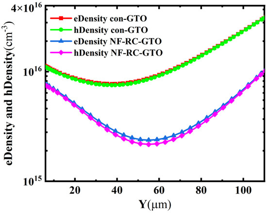
Figure 8. Electron and hole density profiles in the drift region of con-GTO and NF-RC-GTO along the device’s vertical direction during normal turn-on at 15 A/cm2.
Generally, GTOs are characterized by stringent shutdown conditions and high turn-off losses. Figure 9 illustrates the correlation between the turn-off time and turn-off energy loss of the NF-RC-GTO and LD at 8000 V and 15 A/cm2, along with a comparison to traditional GTOs.
The figure indicates a decrease in both turn-off time and loss as the LD value increases. Notably, when LD exceeds 8 µm, there is a plateau in both turn-off time and loss, with minimal further changes observed. In comparison to standard GTOs, the turn-off time of the NF-RC-GTO is reduced by over 80%, and the turn-off loss is cut by more than 85%. These findings confirm the NF-RC-GTO’s enhanced capability in reducing both turn-off time and loss, particularly in operations involving lower currents.
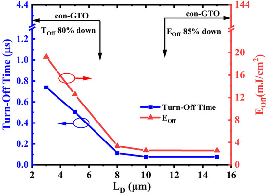
Figure 9. Turn-off time and turn-off energy of NF-RC-GTO at different LD.
4. Conclusions
In summary, we have proposed a SiC NF-RC-GTO design, incorporating an N-float layer at the cell’s bottom. Experiments conducted with TCAD simulation software have shown that an optimal setting of the NF structure’s shape and doping concentration parameters can significantly reduce the snapback effect. When the thickness of the NF structure exceeds 4 µm and the doping concentration is set to 2 × 1014 cm−3, the snapback effect is completely eliminated.
Furthermore, the breakdown voltage of the proposed NF-RC-GTO has been improved by 11.4% compared to conventional GTOs. More importantly, at specific low current densities, it can reduce turn-off time by 80% and turn-off losses by 85%, indicating this design’s significant potential in reducing losses. Our next step in the research plan involves studying the thermal management capabilities of the NF-RC-GTO and investigating the manufacturing process flow of the NF-RC-GTO.
Authors
Chengcheng Wu ,Juntao Li, Zhiqiang Li, Lin Zhang, Kun Zhou, Xiaochuan Deng.
Original – MDPI
-

STMicroelectronics announced a collaboration with Compuware Technology Inc, (Compuware), a leading provider of high-efficiency power supplies, on a reference design for server power using ST’s industry-leading silicon carbide (SiC), galvanic isolation, and microcontroller technologies. This reference design provides unparalleled power-supply options for digital power converter applications including server, datacenter and telecom power.
As demand for digital services continues to grow, fueled by Artificial Intelligence (AI), 5G, and the Internet of Things (IoT), keeping power usage under control is an important piece of the sustainability puzzle for data centers. The STDES-3KWTLCP reference design is perfect for a 3kW and higher wattage CRPS (Common Redundancy Power Supply) server power supply. This technical advancement comes with superior efficiency, faster switching, reduced energy losses, and better thermal management capabilities. In addition, this total system solution shortens time-to-market.
Compuware stands as a global power supply leader, holding the world record for the highest number of 80 PLUS Titanium certifications, ensuring unparalleled power efficiency. Engineered for excellence, Compuware power solutions are the ideal choice for HPC, AI, Deep Learning, Cloud, and advanced applications. With high power density, it optimizes space usage without compromising reliability and efficiency, setting a new performance standard in demanding computing environments.
“Combining ST’s latest SiC MOSFET, galvanic isolation, and microcontroller technologies with Compuware’s leading-edge power energy expertise is helping Compuware unleash our design creativity to develop high-density and -efficiency solutions. Now we can achieve 89W/in.3 power density, a small size, and high power output, this reference design is a great choice for power-hungry, high-performance computing applications,” according to Robin Cheng, Vice President at Compuware.
“With a focus on the Industrial market, ST’s Power & Energy Competence Center provides low-power, mid-power, and high-power solutions with the most advanced ST technologies to our customers, and this reference design- STDES-3KWTLCP can help our customers increase energy efficiency and reduce time-to-market using ST’s efficient and reliable power solutions,” said Eric Chou, Head of Power & Energy Competence Center at STMicroelectronics.
Original – STMicroelectronics
-
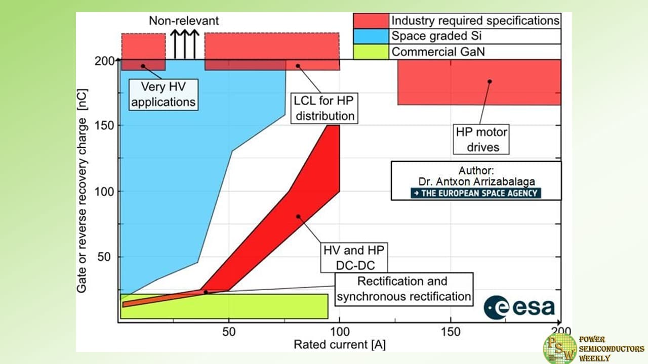
Recently the European Space Agency (ESA) started its search for the technological advantage to improve their systems. Lead by research fellow Dr. Antxon Arrizabalaga, the project is aimed at studying the latest semiconductor technologies and exploring the impact they can have in the future of the space industry.
During its research, Dr. Antxon Arrizabalaga is looking forward to answer the following questions:
- Which are the next system-level figures the space power industry wants to achieve?
- Can the wide bandgap semiconductors help to achieve these figures?
- Which semiconductor ratings are demanded by the space power industry for each application?
At the moment the research project lead by Dr. Arrizabalaga is focusing on the silicon carbide (SiC) power semiconductor devices, as they are better suited for the requirements of the high-power applications. The team has already had several meetings with the main European space power companies discussing the points of interest mentioned above.
As a result, ESA received rich feedback with industry requirements and new ideas. And as anticipated, most of the companies are looking to the ways to increase power of their systems.
Thus, the following applications were mentioned the most:
- Latching current limiters (LCL) for high power distribution
- High-voltage (HV), increasing the traditional bus voltage, and high-power (HP) DC-DC converters
- Rectification and synchronous rectification
- HP motor drives
- Very HV applications, around and over 1 kV
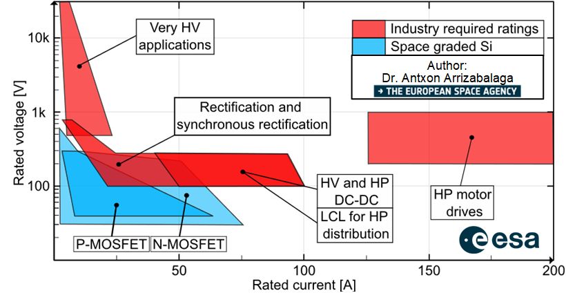
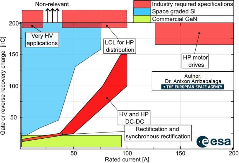
Figure 1. The ratings of the semiconductor devices required by the industry for each application
According to Dr. Arrizabalaga, ESA classifies innovations in three categories, according to the degree of innovation they bring when compared to the state-of-the-art:
- Enhancing. It brings a substantial improvement to the state-of-the-art system.
- Based on a technology replacement
- For SiC devices it means replacing the Si devices in an existing application and optimizing the system to get system-level benefits
- Low risk, development time and cost for manufacturers
- Straightforward adoption by industry and high probability of success
- Enabling. It will allow a new feature, new application, or even a new mission.
- Critical technologies for a certain feature, application or mission
- For SiC devices it means that without the adoption of such devices, the new desired feature, application or mission is no longer possible
- Medium-high risk for manufacturers, higher development cost and effort, since it has never been done before
- More challenging adoption by industry, and lower probability of success
- Game-changing. It promises to bring entirely new capabilities (not considered for this study).
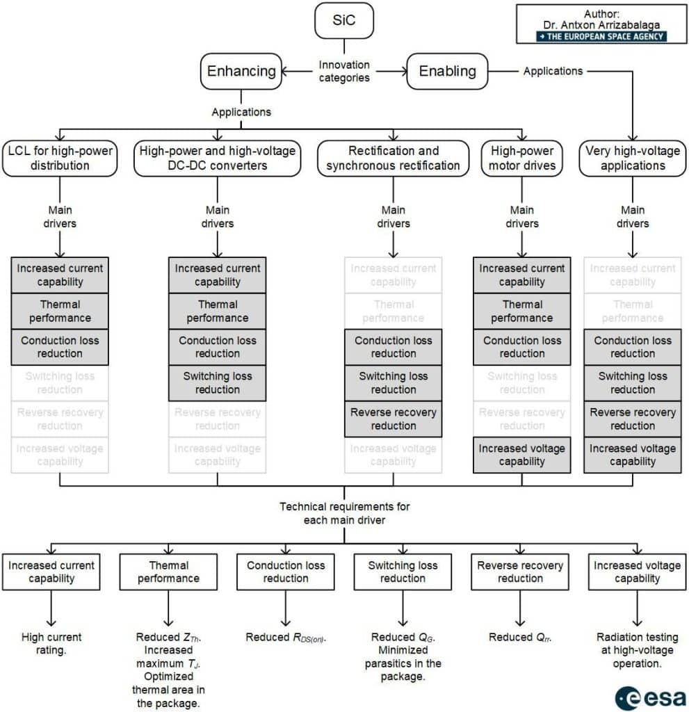
Figure 2. Classification of the applications mentioned by the industry and the main drivers needed to be optimized for each application.
The European Space Agency research team is looking forward to support the successful adoption of the wide bandgap (WBG) power semiconductor devices by the European space power industry, giving the European industry a competitive edge.
Original – Dr. Antxon Arrizabalaga
