-
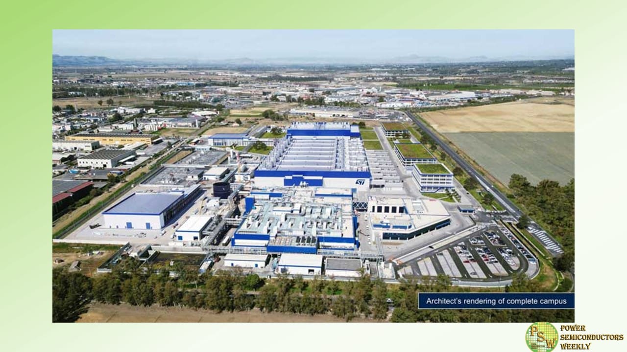
STMicroelectronics announced a new high-volume 200mm silicon carbide (“SiC”) manufacturing facility for power devices and modules, as well as test and packaging, to be built in Catania, Italy. Combined with the SiC substrate manufacturing facility being readied on the same site, these facilities will form ST’s Silicon Carbide Campus, realizing the Company’s vision of a fully vertically integrated manufacturing facility for the mass production of SiC on one site.
The creation of the new Silicon Carbide Campus is a key milestone to support customers for SiC devices across automotive, industrial and cloud infrastructure applications, as they transition to electrification and seek higher efficiency.
“The fully integrated capabilities unlocked by the Silicon Carbide Campus in Catania will contribute significantly to ST’s SiC technology leadership for automotive and industrial customers through the next decades,” said Jean-Marc Chery, President and Chief Executive Officer of STMicroelectronics. “The scale and synergies offered by this project will enable us to better innovate with high-volume manufacturing capacity, to the benefit of our European and global customers as they transition to electrification and seek more energy efficient solutions to meet their decarbonization goals.”
The Silicon Carbide Campus will serve as the center of ST’s global SiC ecosystem, integrating all steps in the production flow, including SiC substrate development, epitaxial growth processes, 200mm front-end wafer fabrication and module back-end assembly, as well as process R&D, product design, advanced R&D labs for dies, power systems and modules, and full packaging capabilities. This will achieve a first of a kind in Europe for the mass production of 200mm SiC wafers with each step of the process – substrate, epitaxy & front-end, and back-end – using 200 mm technologies for enhanced yields and performances.
The new facility is targeted to start production in 2026 and to ramp to full capacity by 2033, with up to 15,000 wafers per week at full build-out. The total investment is expected to be around five billion euros, with a support of around two billion euros provided by the State of Italy within the framework of the EU Chips Act. Sustainable practices are integral to the design, development, and operation of the Silicon Carbide Campus to ensure the responsible consumption of resources including water and power.
Original – STMicroelectronics
-
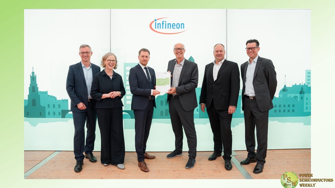
Infineon Technologies AG is on schedule with the construction of the Smart Power Fab in Dresden and is initiating the final construction phase. During a visit, the Prime Minister of the Free State of Saxony, Michael Kretschmer, officially handed over the last outstanding building permit for the new fab issued by the State Directorate of Saxony.
The excavation of the building pit has now been completed. The shell and building construction are currently progressing on the concrete foundation, which is up to two meters thick. Infineon officially broke ground for the new plant in Dresden in May 2023. Manufacturing is scheduled to start in 2026. The production will focus on semiconductors that promote decarbonization and digitalization.
With a total investment of five billion euros, the company is making a significant contribution to the European Commission goal to increase the EU’s share of global semiconductor production to 20 percent by 2030. The semiconductors manufactured in Dresden will secure future value chains in key European industries. The products manufactured in the new production facility will be used in the automotive and renewable energy industries. The interaction of power semiconductors and analog/mixed-signal components enables particularly energy-efficient and intelligent system solutions – hence the name Smart Power Fab.
“The construction of the Smart Power Fab is a big win for Dresden, Saxony, Germany and Europe,” says Michael Kretschmer, Prime Minister of the Free State of Saxony. “Infineon’s fourth production module in Dresden is another important building block in strengthening Europe’s resilience in the field of microelectronics. It is a further step towards achieving the European Commission’s goal of increasing Europe’s share of global chip production to 20 percent. Thanks to a thoughtful cooperation between the company, the Free State of Saxony, the local authorities, and the federal government, it has been possible to get the investment off the ground and to issue the relevant permits quickly. As a result, the semiconductors that we urgently need for the mobility and energy transition can be produced in the new fab starting in 2026.”
“We are making excellent progress with the construction of our state-of-the-art Smart Power Fab in Dresden. We are right on schedule also thanks to the excellent cooperation with the authorities,” says Dr. Rutger Wijburg, Member of the Management Board and Chief Operations Officer of Infineon. “With our strategic decision to continue investing in Dresden, we are securing the long-term future of the site and strengthening the manufacturing base for semiconductors in Europe.”
The dimensions of the construction site are impressive. On average, construction workers have removed around 8,000 tons of soil every day since the start of work. A total of 450,000 cubic meters of excavated soil has been produced, which corresponds to the volume of 180 Olympic swimming pools.
The soil is being temporarily stored in a specially prepared area near the Dresden Airport freeway junction. The 22-metre-deep pit not only compensates for the natural gradient, but also provides a firm foundation for the 150- to 190-centimetre-thick base plate, which is intended to reduce vibrations – from passing streetcars, for example – to a minimum. Even minimal vibrations can affect the sensitive semiconductor production.
In the next construction phase, the basement levels will be built, along with other levels. The clean room – the heart of the Smart Power Fab – is planned for the fourth level. Once completed, it will be at the exact same height as the site’s three existing production rooms. This will optimize an integrated production. The future construction phase of the project includes a total of ten tower cranes, some of them 80 meters high to support up to 1,200 construction workers who will be working on the site every day in multiple shifts.
The investment in Dresden is part of the company’s strategy to reach CO 2-neutrality by 2030. The Smart Power Fab sets new efficiency standards for the consumption of important resources such as energy and water. This has a positive impact on the carbon footprint of Infineon. Even today, Infineon’s products, which are used in solar and wind power plants, reduce 34 times the amount of CO 2 emitted during their production over their lifetime.
With the investment in the new plant, Infineon is creating an additional 1,000 jobs in the Saxon state capital. The company currently employs approximately 3,250 people in Dresden. The number of trainees has already been significantly increased with the new Fab. Subject to the European Commission’s state aid decision and the national grant procedure, the project is to be funded in accordance with the objectives of the European Chips Act. Infineon is aiming for public funding of around one billion euros.
Original – Infineon Technologies
-
Cambridge GaN Devices (CGD) has signed a Memorandum of Understanding with Industrial Technology Research Institute (ITRI) of Taiwan to solidify a partnership in developing high performance GaN solutions for USB-PD adaptors. The MoU also covers the sharing of domestic and international market information, joint visits to potential customers and promotion.
Andrea Bricconi | Chief Commercial Officer, CGD
“We are excited to partner with ITRI, an organization with a power solution research team that is very experienced in developing power solutions and holds many patents. We will be demonstrating some of their board designs at our booth at the upcoming PCIM show in Nuremberg in June. These products utilize CGD’s unique IC chip architecture and ITRI’s patented designs to achieve product size reduction, high efficiency and power density, and cost competitiveness.”
Wen-Tien Tsai | leader of Commercial Power Design team, GEL/itri
“CGD’s IC-enhanced GaN – ICeGaN – is a novel platform that improves ease-of-use, facilitates smart temperature control and enhances gate reliability. We are excited to include these benefits in our new power designs.”
According to leading WBG analysts, Yole Group, the GaN market is expected to exceed $1B, with key growth in the applications of comms power supplies, and automotive DC/DC converters and on-board chargers. However, the first commercialized product in the market to adopt GaN devices has been USB-PD adaptors, and it is this market that the first designs from the partnership will address. Specifically, the agreement covers the development of power solutions in the 140-240 W range with power densities exceeding 30 W/in3 for e-mobility, power tools, notebook and cell phone applications.
Original – Cambridge GaN Devices
-
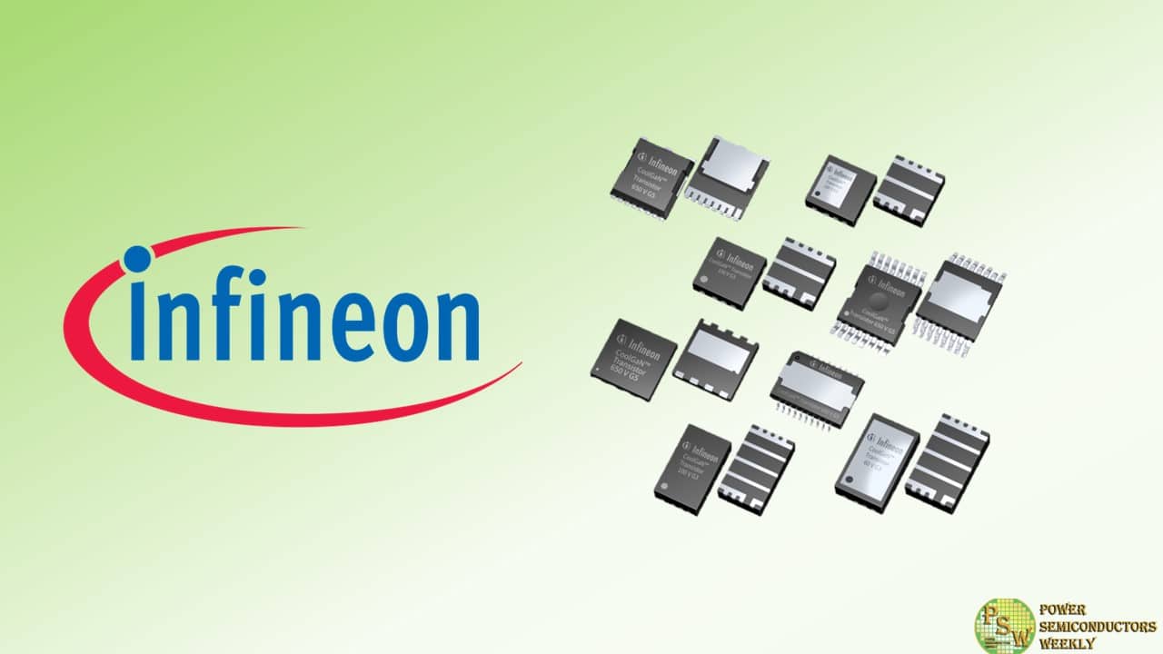
Infineon Technologies AG announced two new generations of high voltage (HV) and medium voltage (MV) CoolGaN TM devices which now enable customers to use Gallium Nitride (GaN) in voltage classes from 40 V to 700 V in a broader array of applications that help drive digitalization and decarbonization.
These two product families are manufactured on high performance 8-inch in-house foundry processes in Kulim (Malaysia) and Villach (Austria). With this, Infineon expands its CoolGaN advantages and capacity to ensure a robust supply chain in the GaN devices market, which is estimated to grow with an average annual growth rate (CAGR) of 46 percent over the next five years according to Yole Group.
“Today’s announcement builds nicely on our acquisition of GaN Systems last year and brings to market a whole new level of efficiency and performance for our customers,” said Adam White, Division President of Power & Sensor Systems at Infineon. “The new generations of our Infineon CoolGaN family in high and medium voltage demonstrate our product advantages and are manufactured entirely on 8 inch, demonstrating the fast scalability of GaN to larger wafer diameters. I am excited to see all of the disruptive applications our customers unleash with these new generations of GaN.”
The new 650 V G5 family addresses applications in consumer, data center, industrial and solar. These products are the next generation of GIT-based high voltage products from Infineon. The second new family manufactured on the 8-inch process is the medium voltage G3 devices which include CoolGaN Transistor voltage classes 60 V, 80 V, 100 V and 120 V; and 40 V bidirectional switch (BDS) devices. The medium voltage G3 products are targeted at motor drive, telecom, data center, solar and consumer applications.
The CoolGaN 650 V G5 will be available in Q4 2024 and the medium voltage CoolGaN G3 will be available in Q3 2024. Samples are available now.
Original – Infineon Technologies
-

CVD Equipment Corporation appointed Andrew Africk to its Board of Directors. The Board of Directors also approved an expansion of the number of directors from the current level of six to seven.
“We are delighted that Mr. Africk has agreed to join our Board,” said Lawrence J. Waldman, Chairman of CVD Equipment Corporation’s Board of Directors. “We appreciate his support of the company as our largest shareholder, and we welcome his extensive corporate and financial experience that will be invaluable to our Board of Directors and executive management team.”
Mr. Africk is the founder of Searay Capital LLC, a private investment company. Mr. Africk established Searay Capital in July 2013 after 21 years leading private equity and capital markets investments for Apollo Global Management. As a Senior Partner at Apollo, Mr. Africk was responsible for investments in technology and communications, and he has 30 years of experience financing, analyzing and investing in public and private companies. Mr. Africk graduated from UCLA with a B.A. in Economics, from the University of Pennsylvania Law School with a J.D., and from the University of Pennsylvania’s Wharton School of Business with an MBA.
Manny Lakios, President and CEO of CVD Equipment Corporation, also commented, “I am very pleased to have Mr. Africk join our Board of Directors. His in-depth knowledge of the technology sector will add an additional perspective and allow him to contribute as a member of the Board of Directors strategically as we focus on key markets of high power electronics, battery materials, aerospace and industrial applications.”
Original – CVD Equipment
-

In a significant advancement for the high-voltage power electronics industry, Maspower Semiconductor has introduced the MS2N300HGC0 MOSFET, a powerful new component that sets new benchmarks in performance and reliability.
This cutting-edge product, housed in the TO-247 package, offers unprecedented performance with its robust 3000V voltage rating and 2A continuous current capability. What truly sets this MOSFET apart, however, is its rigorous testing and certification. The MS2N300HGC0 has undergone 100% avalanche testing, ensuring exceptional resilience and durability in demanding applications.
Moreover, the MS2N300HGC0’s Fast Intrinsic Diode design and minimized gate charge contribute to its high-speed switching capabilities, making it a perfect fit for high-voltage power supplies, PV inverters, switching applications and more. Its very low intrinsic capacitance further enhance its performance, delivering maximum efficiency and reliability. Maspower’s commitment to innovation and reliability is evident in the MS2N300HGC0, which has been rigorously tested and certified to meet the highest industry standards.
“The MS2N300HGC0 is a testament to our commitment to pushing the boundaries of high-voltage power electronics,” said a spokesperson from Maspower. “We are proud to offer this state-of-the-art MOSFET to our customers, enabling them to achieve unprecedented levels of performance and reliability in their applications.”
Original – Maspower Semiconductor
-

At PCIM Europe 2024, Infineon Technologies AG will showcase how its latest semiconductor, software, and tooling solutions provide answers to today’s green and digital transformation challenges. Under the motto “Driving decarbonization and digitalization. Together.”, Infineon will demonstrate the industry’s broadest power electronics portfolio covering all relevant power technologies in silicon (Si), silicon carbide (SiC), and gallium nitride (GaN).
The company will be exhibiting in a larger area this year, with the main booth #740 in Hall 7 demonstrating innovative Si and SiC-based solutions, while the adjacent booth #169 is dedicated to the broad GaN portfolio. Alternatively, visitors can also register for Infineon’s digital event platform.
Infineon’s PCIM 2024 highlights
The products, demonstrations, and design aids on display illustrate how Infineon’s product-to-system expertise in power management enables engineers to balance operational specifications with application requirements. Demonstrations will include solutions from the following areas:
- Wide-bandgap technologies: Wide-bandgap materials are revolutionizing power electronics and various applications that are driving the green and digital transformation. Infineon will demonstrate the CoolSiC™ MOSFETs 650 V and 1200 V Generation 2, which can be used to improve overall energy efficiency. Additionally, the expanded portfolio of GaN solutions will be showcased, offering a wide range of innovative packages, discrete and integrated solutions.
- Renewables, energy storage and HVDC: With its power solutions, Infineon enables the most climate-friendly forms of energy generation from wind and solar accompanied by efficient storage systems. At PCIM, the company will present a wide range of solutions for single-phase and three-phase hybrid solar inverters as well as its In-Field Power Analytics Service helping to maximize converter uptime and optimize operation in real-time.
- Industrial automation, motor drives and control: With advanced power semiconductors, Infineon is paving the way for highly reliable and energy-efficient electric motors and drive solutions in smart factories. This is achieved through a combination of efficient energy management and intelligent motor control solutions, advanced sensor functions, and reliable connectivity components. Furthermore, the company is presenting its growing range of solid-state relays and circuit breakers as well as a stack assembly solution for high-end Press Pack IGBTs.
- Information and communication technologies: True to the motto “We power AI”, Infineon exhibits innovative technologies that make it possible to meet increasing energy demands while promoting greener AI and paving the way for more efficient AI servers. This includes two-phase power supply modules, integrated point-of-load solutions, and converters. In addition, the company will showcase cutting-edge solutions, including Si, SiC, and GaN power switches, that meet the evolving needs of server technology and telecoms networks, driving efficiency, reliability, and innovation across all industries.
- eMobility, eTransportation and charging solutions: With leading power supply solutions for traction inverters, on-board chargers, DC-DC converters, and battery management systems, Infineon supports the efforts of developers and manufacturers, enabling the rapid expansion of eMobility, eTransportation, eCAV, and the corresponding charging infrastructure. Highlights presented in this area include traction inverters with fusion, single-side cooling and discrete concepts, traction inverter systems for commercial vehicles and rail transport, as well as high power fast charging solutions.
- Smart and connected homes: Infineon’s leading technology portfolio of customized, ready-to-use solutions assists manufacturers in developing innovative system designs for homes that meet the growing demand for smart, connected, and energy-efficient living solutions. Highlights in this area include USB-C charging solutions, portable battery-powered welding solutions, residential heat pumps, as well as air conditioning systems.
Infineon will also contribute to the PCIM conference program and the various forums, including a keynote by Dr. Gerald Deboy, Fellow at Infineon, on the “Challenges and Solutions to Power Latest Processor Generations for Hyper Scale Data Centers” on June 13 at 8:45 am. An overview of all contributions by Infineon experts is available at www.infineon.com/pcim.
Original – Infineon Technologies
-
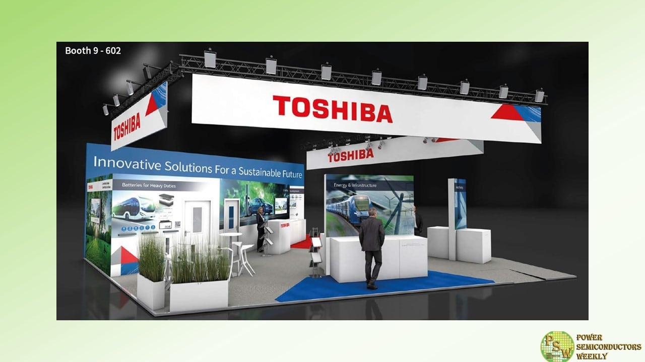
Toshiba Electronics Europe GmbH and Toshiba Materials CO., LTD. will bring solutions that support customers’ goals in reducing their CO2 footprint at the PCIM 2024 conference and exhibition (Nuremberg 11th – 13th June).
This year, the company will use the event to showcase a combination of several business units that support development of sustainable solutions. Semiconductor, battery, and fine ceramic material solutions form a complete chain of products in key applications from e-mobility, industrial, energy and infrastructure sectors.
Toshiba has manufactured top-class ceramics since the 1970s, and its pioneering Silicon Nitride substrates will be on display along with bearing balls, AMOBEADS™, and Nanocrystalline common mode choke cores.
In Toshiba’s eMobility booth area, visitors will discover demonstrations of automotive thermal management by heat pumps and fans utilising Toshiba’s newly released SmartMCD.
Toshiba’s industrial demonstrations highlight the entire product chain from control to isolation to power conversion stages, incorporating the latest generations of SiC, GaN and low-voltage MOSFET technologies. They include reference design implementations utilising modern topologies for factory automation, power supplies, and motor control applications.
Energy and infrastructure demonstrations will focus on high-power solutions such as IEGT and SiC Modules supporting voltages from 1.2kV to 3.3kV. Toshiba’s SiC Cube illustrates a solution implementation for charging infrastructure utilising SiC MOSFET devices, whereas SCiB batteries demonstrate their effective use for energy storage.
Toshiba representatives are also scheduled to participate in the conference program speeches and poster sessions on Wide Bandgap, power semiconductors and gate driver ICs topics.
Original – Toshiba
-
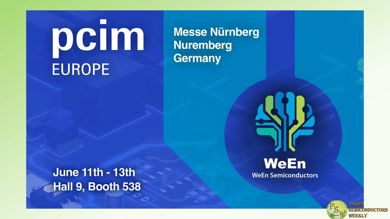
WeEn Semiconductors will be exhibiting the company’s latest highly efficient, high-power density silicon carbide (SiC) technologies, automotive grade power devices and highly reliable IGBTs at PCIM Europe 2024 in Nuremberg from June 11-13, 2024.
Established in 1979, PCIM Europe serves as a premier platform for showcasing the latest advancements in power electronics technologies and applications. This year, in Hall 9, booth 538, under the theme of ‘Power Efficiency for a Cooler Planet,’ WeEn Semiconductors will exhibit its extensive range of high-voltage 1700V SiC power modules, SiC 1200V/750V MOSFETs, Thyristors, power diodes, silicon-controlled rectifiers (SCRs), IGBTs, and other advanced power devices tailored for the renewable energy and e-mobility industries.
With a focus on efficiency, sustainability and cost reduction, WeEn’s broad portfolio offers best-in-class performance, efficiency and density for demanding applications including solar and wind power storage, electric vehicle (EV) fast chargers and traction inverters, HVAC and datacenter servers.
“At WeEn, we are dedicated to developing cost-effective power control technologies that support high voltage ratings and efficient, high-performance operation,” remarked WeEn Semiconductors CEO, Markus Mosen. “We’re excited to showcase the solutions we’ve launched in recent months at PCIM, not least those technologies targeted at renewable energy and electric mobility applications that demonstrate our commitment to products that not only meet but exceed the unique demands of every application while contributing to environmental sustainability.”
PCIM 2024 highlights
- At PCIM, WeEn is set to introduce a range of SiC MOSFETs and SiC Schottky Barrier Diodes (SBDs) in TSPAK packages for EV charging, On Board Charger (OBC), PV inverters, and high power density PSU applications. The new MOSFETs are available in 650V, 750V, 1200V, and 1700V variants, with resistance ranging from 20mΩ to 150mΩ. The current range for the new SiC SBDs is 10 to 40A in 650V, 750V, and 1200V variants.
- A range of SiC power modules in half-bridge, four-pack, six-pack, dual booster, and NPC 3L topologies will also be on display. Target markets for these SiC modules include EV charging, energy storage systems, motor drivers, industrial power supply units (PSUs), test instruments, and PV inverters.
- 1700V SiC series and 1200V / 750V auto-grade SiC MOSFETs, which encompass a diverse range of packaging options and product configurations, including surface-mount device (SMD) discrete components and top-side cooling.
- Highly reliable thyristor/diode modules, suitable for mainstream industrial applications like UPS, Inverter, soft starter, with VDRM up to 1600V and IT(RMS) up to 250A . Thanks for its planar chip technology and state-of-art module manufacture capability, those modules can be in half-bridge, parallel or antiparallel or other customized topology, it has passed 1000 hours reliability test under JEDEC standard as well 100% Pb-Free for the highest level EU RoHS compliance.
- WeEn’s product platforms include Super Junction MOSFETs with breakdown voltage ranges of 600V, 650V, and 800V. Leveraging advanced 8-inch wafer technology, WeEn offers a wide range of trench MOSFETs with voltage ranges from 20V to 30V.
- With voltage ratings from 45V to 2000V, WeEn’s Power Diodes feature current ratings from 1A to 100A. The company’s product portfolio includes low VF Schottky rectifiers, standard diodes, and ultrafast recovery rectifiers.
- WeEn’s range of IGBTs boasts extremely low leakage currents and exceptional conduction and switching characteristics at both high and low junction temperatures. They have undergone high voltage H3TRB and 100%-biased HTRB tests with a maximum junction temperature of 175°C safely. These application-specific IGBTs have been tuned to match the precise needs of each application, including switching behaviors, conduction losses, short circuit capabilities, environmental ruggedness, and freewheeling diode characterization. The 1200V and 650V variant current products, including bare dies, discrete components, and PIMs, are offered to various end customers.
Original – WeEn Semiconductors
-
With the increasing power requirements of Artificial Intelligence (AI) processors, server power supplies (PSUs) must deliver more and more power without exceeding the defined dimensions of the server racks. This is driven by a surge in energy demand of high-level GPUs, which could consume 2 kW and more per chip by the end of the decade.
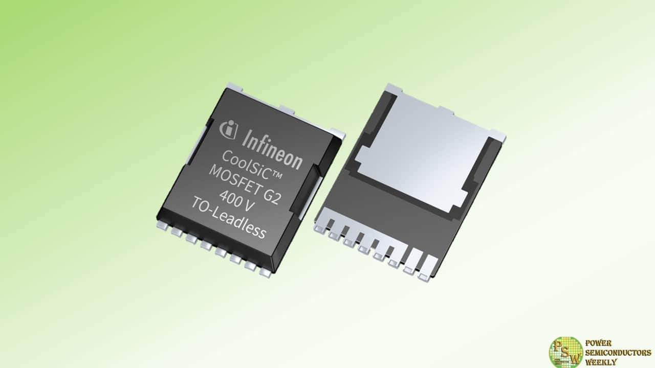
These needs, as well as the emergence of increasingly demanding applications and the associated specific customer requirements have prompted Infineon Technologies AG to extend the development of SiC MOSFETs to voltages below 650 V. The company is now launching the new CoolSiC™ MOSFET 400 V family, which is based on the second generation (G2) CoolSiC technology introduced earlier this year.
The new MOSFET portfolio was specially developed for use in the AC/DC stage of AI servers, complementing Infineon’s recently announced PSU roadmap. The devices are also ideal for solar and energy storage systems (ESS), inverter motor control, industrial and auxiliary power supplies (SMPS) as well as solid-state circuit breakers for residential buildings.
“Infineon offers an extensive portfolio of high-performance MOSFETs and GaN transistors to meet the demanding design and space requirements of AI server power supplies”, said Richard Kuncic, Head of the Power Systems Business Line at Infineon. “We are committed to supporting our customers with advanced products such as the CoolSiC MOSFETs 400 V G2 to drive highest energy efficiency in advanced AI applications.”
The new family features ultra-low conduction and switching losses when compared to existing 650 V SiC and Si MOSFETs. Implemented in a multi-level PFC, the AC/DC stage of the AI Server PSU can attain a power density of more than 100 W/in³ and is proven to reach 99.5 percent efficiency.
This is an efficiency improvement of 0.3 percentage points over solutions using 650 V SiC MOSFETs. In addition, the system solution for AI Server PSUs is completed by implementing CoolGaN™ transistors in the DC/DC stage. With this combination of high-performance MOSFETs and transistors, the power supply can deliver more than 8 kW with an increase in power density by a factor of more than 3 compared to current solutions.
The new MOSFET portfolio comprises a total of 10 products: five R DS(on) classes from 11 to 45 mΩ in Kelvin-source TOLL and D²PAK-7 packages with .XT package interconnect technology. The drain-source breakdown voltage of 400 V at T vj = 25°C. makes them ideal for use in 2- and 3-level converters and for synchronous rectification.
The components offer high robustness under harsh switching conditions and are 100 percent avalanche tested. The highly robust CoolSiC technology in combination with the .XT interconnect technology enables the devices to cope with power peaks and transients caused by sudden changes in the power requirements of the AI processor. Both the connection technology and a low and positive R DS(on) temperature coefficient enable excellent performance under operating conditions with higher junction temperatures.
Original – Infineon Technologies
