-
Like PCIM Europe, which takes place annually in Nuremberg in Germany, the PCIM event in China is an international meeting ground for specialists in power electronics and its applications in drive technologies and power quality. This year PCIM Asia will be held on August 29-31, 2023 in Shanghai.
The event offers a chance to see the latest developments in power electronics components and systems. The strong link between conference and exhibition guarantees the high quality of the show. This unique combination fosters the fast and easy exchange between industry and science, for which PCIM Asia is famous.
This is where experts from industry and academia meet, where new trends and developments are presented to the public for the very first time. In this way, the event mirrors the entire value chain – from components, drives control and packaging to the final intelligent system.
PCIM Asia is an international exhibition and conference focusing on power electronic device industry chain in Asia. It is the first choice platform for domestic and foreign well-known device manufacturers to release new products and latest technologies. A number of enterprises in the field of electronic materials, inductive components and passive component products will debut in PCIM Asia for the first time.
PCIM Asia Conference is highly praised for its in-depth discussion of the latest industrial scientific research achievements with the combination of academics and industries.
Original – PCIM Asia
-
The EPE ECCE Europe conference is one of the largest in the world, attracting around eight hundred experts from numerous countries every year. Aiming at exchanging experience among fellow professionals and academics, and bearing in mind the present and future role of power electronics in the big energy transition the world is looking forward to, the EPE ECCE Europe conference is the privileged place to achieve this goal. EPE’23 ECCE Europe in Aalborg will provide the opportunity to discuss hot topics through the lecture- and poster sessions, the exhibition, the industrial forums and the tutorials.
After a successful EPE ECCE Europe conference in 2007, the Power Electronics community will gather again in Aalborg, Denmark, from September 4 to 8, 2023, to exchange views on research progress and technological developments in the various topics described elsewhere in this website.
On Monday, September 4th, several tutorials will be organized, and some exciting technical visits are planned for Friday, September 8th.
The 25th Conference on Power Electronics and Applications (and Exhibition), EPE ’23 ECCE Europe (Energy Conversion Congress and Expo Europe) is co-sponsored by the EPE Association and the IEEE Power Electronics Society (PELS).
The conference will take place at the AKKC – The Aalborg Congress and Culture Center, in Aalborg, Denmark, and will highlight several Focus Topics:
- Tuesday 5 September:
Energy Islands
1. Renewable Energy Systems and Power-to-X
2. Energy Islands- Wednesday 6 September:
Energy Storage
3. Energy-storage Technologies
4. Electric Vehicles- Thursday 7 September:
Emerging Technologies in Power Electronics
5. Emerging Power Electronic Devices and Semiconductors
6. Reliability and Artificial Intelligence in Power ElectronicsOriginal – EPE’23 ECCE Europe
-
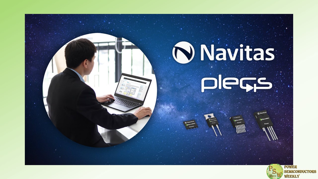
Navitas Semiconductor and Plexim GmbH announced a partnership to release GeneSiC G3™ SiC MOSFET and Gen 5 MPS diode PLECS thermal loss models for highly-accurate simulations of complete power electronics systems.
Power designers can simulate power and thermal losses in various soft- and hard-switching applications. Proprietary GeneSiC trench-assisted planar-gate MOSFET technology delivers the lowest RDS(ON) at high temperature and the highest efficiency at high speeds, and new MPS diodes with ‘low-knee’ characteristics drive unprecedented, industry-leading levels of performance, robustness and quality.
“Accurate, empirically-based simulation models maximize the chance of first-time-accurate designs, accelerating time-to-market and time-to-revenue,” noted Dr. Ranbir Singh, Navitas EVP for the GeneSiC business line. “For the power designer, understanding the leading-edge performance of GeneSiC MOSFETs and MPS diodes with detailed device characteristics, plus power, efficiency and thermal analysis is a critical competitive advantage.”
“The intuitive and highly-efficient PLECS lookup-table based approach to simulating thermal semiconductor losses in complex power electronic circuits is key,” said Kristofer Eberle, Plexim, North America. “Unlike legacy modeling approaches that are not well-suited to new wide bandgap materials, PLECS uses a simplified, but accurate behavioral description to highlight the superior performance of the GeneSiC MOSFETs.”
PLECS models for GeneSiC MOSFETs and MPS diodes are available via genesicsemi.com.
Original – Navitas Semiconductor
-
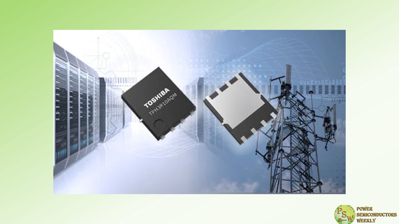
Toshiba Electronic Devices & Storage Corporation (“Toshiba”) has launched “TPH3R10AQM,” a 100V N-channel power MOSFET fabricated with Toshiba’s latest-generation process, U-MOS X-H. The product targets applications such as switching circuits and hot swap circuits on the power lines of industrial equipment used for data centers and communications base stations.
TPH3R10AQM has industry-leading 3.1mΩ maximum drain-source On-resistance, 16% lower than Toshiba’s 100V product, “TPH3R70APL,” which uses the earlier generation process. By the same comparison, TPH3R10AQM has expanded its safe operating area by 76% making it suitable for linear mode operation. Reducing the On-resistance and expanding the linear operating range in the safe operating area reduce the number of parallel connections. Furthermore, its gate threshold voltage range of 2.5V to 3.5V, makes it less likely to malfunction due to gate voltage noise.
The new product uses the highly footprint compatible SOP Advance(N) package.Toshiba will continue to expand its line-up of power MOSFETs that can increase the efficiency of power supplies by reducing loss, and help lower equipment power consumption.
Applications
- Power supplies for communications equipment such as for data centers and communications base stations
- Switching power supplies (High efficiency DC-DC converters, etc.)
Features
- Featuring Industry-leading excellent low On-resistance: RDS(ON)=3.1mΩ (max) (VGS=10V)
- Wide safe operating area
- High channel temperature rating: Tch (max)=175°C
Original – Toshiba
-
Elmos Semiconductor SE, one of the world’s leading suppliers of mixed-signal automotive semiconductors, and Littelfuse, Inc., USA, entered into a definitive agreement on the sale of the Elmos wafer fab at the Dortmund site to Littelfuse. Elmos has agreed to sell the wafer fab at a net purchase price of approximately 93 million Euro. Under the agreement, Littelfuse will acquire the Dortmund wafer fab with a highly skilled technology team of approximately 225 employees. All other activities, including testing operations, will remain with Elmos.
In acquiring the Dortmund wafer fab, Littelfuse enhances its capabilities in power semiconductors for high-growth power conversion applications like renewables, energy storage, and e-Mobility charging infrastructure.
“Today’s agreement is a milestone for semiconductor production in Dortmund and it will strengthen Germany’s standing as a high-tech location. As a fabless company, Elmos will make even greater use of advanced technologies to deliver groundbreaking innovations in mixed-signal semiconductors. Elmos is already the global market leader for certain applications in the automotive industry. We want to use this strong position to shape our future growth,” says Dr. Arne Schneider, CEO of Elmos Semiconductor SE.
Headquartered in Chicago, Illinois, United States, Littelfuse, Inc. is a diversified, industrial technology manufacturing company empowering a sustainable, connected and safer world. The company operates across more than 20 countries, and with approximately 18,000 global associates. Its products are found in a variety of industrial, transportation and electronics end markets. In Germany, Littelfuse operates various manufacturing, sales and R&D sites.
The closing of the transaction is expected to be effective December 31, 2024, and is subject to certain closing conditions and regulatory approvals, among them the investment control procedure under foreign trade law conducted by the German Federal Ministry for Economic Affairs and Climate Action. Elmos will retain full operational control over the wafer fab until the closing date.
In addition, Elmos and Littelfuse have agreed to enter into a defined multi-year capacity sharing arrangement with an initial term lasting through 2029, with Elmos buying defined volumes of wafers produced at the fab. This long-term agreement supplements the existing supply arrangements with Elmos’ other foundry partners and ensures that Elmos has the necessary capacities to meet projected customer demand.
“This is good news for the Elmos wafer fab team. We are delighted for Littelfuse to further develop the wafer fab in Dortmund for power semiconductors. Our employees are now expecting a quick review procedure by the relevant authorities,” says Dr. Schneider.
Following regulatory approvals of the transaction, the buyer will make a payment of approximately 37 million Euro. The remainder of the purchase price will be paid at closing. The transaction has no major effects on EBIT in fiscal year 2023, which is why the current forecast for the full-year EBIT margin in 2023 (25% ± 2 percentage points) continues to apply.
Cash flow is expected to be positively influenced in fiscal year 2023 by the payment of approximately 37 million Euro after regulatory approvals. Irrespective of the transaction, Elmos continues to increase its efforts to expand testing capacities for future growth. The company now anticipates capital expenditures of approximately 19% ± 2 percentage points of sales in fiscal year 2023 (previously: 17% ± 2 percentage points). As a result, Elmos now expects a negative operating adjusted free cash flow in 2023.
Original – Elmos Semiconductor
-

Kulicke and Soffa Industries, Inc. announced the launch of several new systems and capabilities serving high-volume semiconductor and fast-growing power-semiconductor applications.
POWERCOMM™ and POWERNEXX™ represent the next evolution in advanced wire bonding systems and are designed with a new generation of intuitive advanced process capabilities which deliver maximum levels of performance, efficiency, and productivity. Additionally, both systems deliver enhanced mean time between assists (MTBA), with automated recovery features that improve the machine to operator ratio and better support localization of semiconductor assembly.
The POWERCOMM™ advanced wire bonding solution is designed to support high-volume discrete and low-pin count devices commonly used in applications such as data centers, automotive, industrial automation, smartphones, wearables and connected devices.
The POWERNEXX™ advanced wire bonding solution is optimized for higher density QFN packages with widths of up to 100mm. The improved illumination design on POWERNEXX™ allows faster alignment time through its Pattern Recognition System (PRS). Faster alignment and advanced process capabilities deliver the industry leading UPH and lowest Cost-of-Ownership.
In addition to the new POWERCOMM™ and POWERNEXX™ systems, K&S extends its leadership in wedge bond applications with new High-Power-Interconnect (HPI) capabilities addressing the emerging needs of power devices. HPI capabilities are becoming increasingly necessary to assemble applications such as inverters, battery assembly and charging infrastructure which support the growth and increasing efficiency requirements of sustainable energy and electric vehicle applications. The need for more efficient and higher-current applications are driving rapid changes to the power semiconductor market by increasing demand in emerging compound semiconductors, such as Silicon Carbide (SiC) and Gallium Nitride (GaN), but are also demanding new capabilities to support next-generation battery assembly and are accelerating the transition from aluminum wire and ribbon, to copper wire and ribbon. Next generation HPI capabilities are being introduced across Kulicke & Soffa’s leading wedge bonder portfolio today.
“Our rich history of innovation and ongoing development priorities are enabling us to provide additional value to the increasingly critical assembly process. This recent set of new wire bonding systems and capabilities will better enable customers to optimize productivity, improve material handling capabilities and significantly lower cost-of-ownership,” said Shawn Sarbacker, Kulicke and Soffa’s Vice President of Ball Bonder Business Unit.
Original – Kulicke and Soffa Industries
-

ORC Manufacturing Co., Ltd. and Resonac Corporation announced that ORC Manufacturing has taken part in the “JOINT2 (Jisso Open Innovation Network of Tops 2)” consortium, which was established under the leadership of Resonac with the aim of developing next-generation semiconductor packaging technologies. As a result, JOINT2 has become a consortium comprised of 13 leading companies in Japan who manufacture semiconductor packaging materials, substrates, and equipment.
As a consortium which has end-to-end testing line of leading-edge technologies covering back-end processes of semiconductor package manufacturing, JOINT2 will accelerate development of technologies for evaluation and manufacturing of next-generation semiconductor packages.
JOINT2 was established in 2021 as a consortium of 12 companies with the aim of establishing next generation semiconductor packaging technologies and evaluation technologies, including 2.5D and 3D packaging through collaboration among member companies. JOINT2 is the successor of “JOINT” consortium, which was established in 2018.
The combination of the member companies’ materials and equipment allows materials and equipment to be evaluated under conditions similar to the semiconductor evaluation tests conducted by customers. This arrangement helps customers save the time and trouble of carrying out individual evaluations for their suppliers and thereby respond to the need of speedy development of semiconductor packages.
Technologies for “back-end processes” of semiconductor-integrated-circuit manufacturing, where semiconductor chips are packaged, are now required to evolve into next-generation technologies that can support 5G and post-5G high-speed data communication systems. Back-end processes consist of many processes, and consume various materials.
Therefore, back-end processes have many technical issues to be solved, and solutions for these issues require collaboration among many companies. Therefore, Japanese manufacturers have large shares in the field of back-end processes of semiconductor package manufacturing because they are good at comparing and adjusting technologies.
ORC Manufacturing is an equipment manufacturer which has forte in optical technologies, and its key product is direct imaging (Dl) system for production of high-density semiconductor packaging substrates. ORC Manufacturing is now developing next-generation Dl system for back-end processes of semiconductor packaging as a part of the project adopted by the New Energy and Industrial Technology Development Organization (NEDO).
ORC Manufacturing’s participation in JOINT2 reinforces the consortium’s end-to-end testing line of leading-edge back-end process technologies. ORC Manufacturing’s Dl system, which does not require photo-mask preparation, is expected to shorten time-to-market of semiconductor packages, and accelerate technological innovations in back-end processes of semiconductor packaging.
Through its participation in JOINT2, ORC Manufacturing aims to acquire wide-ranging knowledge about back-end processes of semiconductor packaging including process evaluation technologies applicable to pre-imaging through post-imaging, thereby strengthen its capability to offer values to customers.
JOINT2 welcomes the new member, and will further promote open innovation and accelerate the development of more sophisticated evaluation technologies, materials, substrates, and equipment applicable to next-generation semiconductor packaging technologies.
Original – Resonac
-
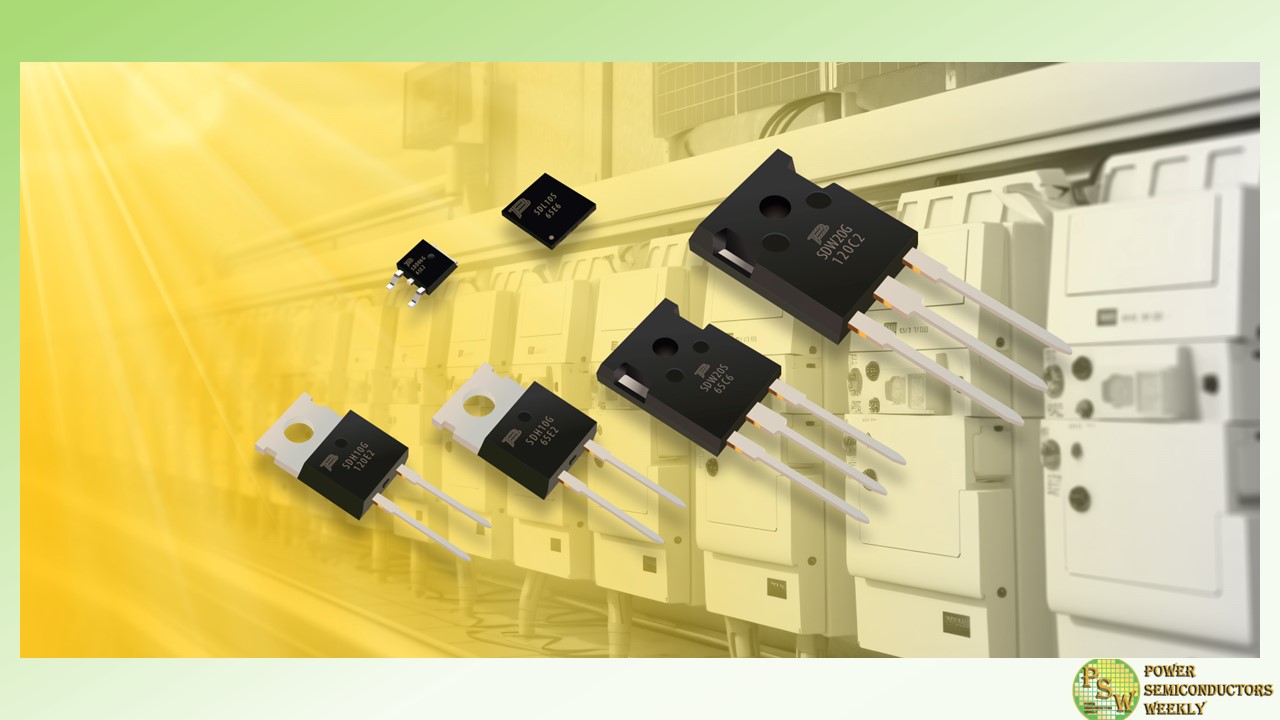
Bourns, Inc. announced its first 650 V – 1200 V Silicon Carbide (SiC) Schottky Barrier Diodes (SBDs). The Bourns® SiC SBD line consists of six models engineered to provide excellent current carrying and thermal capabilities and high power density for increased performance and reliability. These capabilities make Bourns® SiC SBDs optimal high efficiency power conversion solutions for the growing variety of high frequency applications that need to meet reduced size and lower system cost requirements.
Telecom/Server Switched-Mode Power Supplies (SMPS), photovoltaic inverters, PC power and motor drives are a few of the applications that can benefit from the features provided in the Bourns® BSD Series SiC SBDs.
To address ongoing design demands for ever higher power efficiency, Bourns® SiC SBDs feature low forward voltage (VF) and high thermal conductivity, which increases efficiency while lowering power dissipation, satisfying application requirements of 650 V and 1200 V solutions.
The series also has no reverse recovery current to reduce EMI, enabling these SiC SBDs to significantly lower energy losses. In addition to offering 650 V to 1200 V operation with currents in the 6-10 A range, the six new BSD models of wide band gap diodes from Bourns offer designers various forward voltage, current and package options including TO220-2, TO247-3, TO252, and DFN8x8.
The six Bourns® Model BSD SiC SBDs are available now. These models are RoHS compliant, halogen free, Pb free and their epoxy potting compound is flame retardant to the UL 94V-0 standard.
For more detailed product information, please see: www.bourns.com/products/diodes/silicon-carbide-sic-schottky-barrier-diodes
Original – Bourns
-
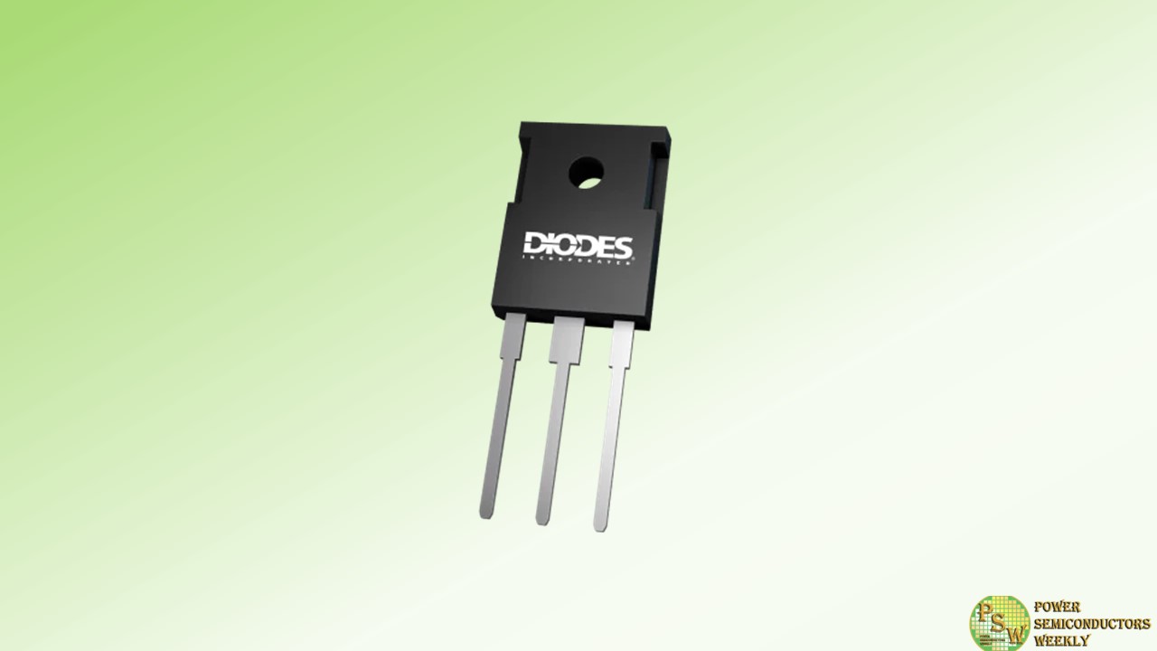
Diodes Incorporated announced a further enhancement of its wide-bandgap product offering with the release of the DMWSH120H90SM4Q and DMWSH120H28SM4Q automotive-compliant Silicon Carbide (SiC) MOSFETs. These N-channel MOSFETs respond to the increasing market demand for SiC solutions that enable better efficiency and higher power density in electric and hybrid-electric vehicle (EV/HEV) automotive subsystems like battery chargers, on-board chargers (OBC), high-efficiency DC-DC converters, motor drivers, and traction inverters.
The DMWSH120H90SM4Q operates safely and reliably up to 1200VDS with a gate-source voltage (Vgs) of +15/-4V and has an RDS(ON) of 75mΩ (typical) at 15Vgs. This device is designed for OBCs, automotive motor drivers, DC-DC converters in EV/HEV, and battery charging systems.
The DMWSH120H28SM4Q operates at up to 1200VDS, +15/-4Vgs, and has a lower RDS(ON) of 20 mΩ (typical) at 15Vgs. This MOSFET has been designed for motor drivers, EV traction inverters, and DC-DC converters in other EV/HEV subsystems. Low RDS(ON) enables these MOSFETs to run cooler in applications that require high power density.
Both products have low thermal conductivity (RθJC=0.6°C/W), enabling drain currents up to 40A in the DMWSH120H90SM4Q and 100A in the DMWSH120H28SM4Q. They also have fast intrinsic and robust body diodes with low reverse recovery charge (Qrr) of 108.52nC in the DMWSH120H90SM4Q and 317.93nC in the DMWSH120H28SM4Q. This enables them to perform fast switching with reduced power losses.
By using the planar manufacturing process, Diodes has created new MOSFETs that offer more robust and reliable performance in automotive applications—and with increased drain current, breakdown voltage, junction temperature, and power rings as compared to previously released versions. The devices are available in a TO247-4 (Type WH) package, which offers an additional Kelvin sense pin. This can be connected to the source to optimize switching performance, enabling even higher power densities.
Original – Diodes Incorporated
-

Wolfspeed, Inc. announced a $1.25 billion secured note financing from an investment group led by Apollo, with an accordion feature for up to an additional $750 million.
The financing supports the company’s previously announced U.S. expansion efforts and is a significant step toward achieving the company’s $6.5 billion global capacity expansion plan. Execution of Wolfspeed’s U.S. growth plan will accelerate adoption of silicon carbide across a wide array of end markets and support meaningful job creation in US semiconductor manufacturing.
The 9.875% notes will mature in 2030 and are optionally prepayable by the company based on the terms of the indenture governing the notes. The investment was led by funds managed by Apollo’s ~$450 billion Credit business.
“The group’s commitment to Wolfspeed further validates the importance of silicon carbide to the global energy transition,” said Gregg Lowe, president and chief executive officer of Wolfspeed. “This important step in our financing provides significant capital to scale up near-term operations at our Mohawk Valley Fab and construction of our Siler City materials facility to help us capture the growing silicon carbide market opportunity. The financing positions Wolfspeed to continue to lead the growth of the industry and focus on the execution of our vertically integrated strategy to meet growing demand.”
“Our agreement with Apollo and its capital partners achieves our near-term funding targets while prioritizing our shareholders with a new, non-dilutive source of financing,” said Neill Reynolds, chief financial officer of Wolfspeed. “Apollo and its capital partners’ investment follows an extensive review of our business and demonstrates their conviction in our team, operating plan and trajectory.”
“Apollo is pleased to provide a dynamic and flexible credit solution to Wolfspeed as it significantly expands its silicon carbide manufacturing capacity. The company’s growth plan is designed to deliver critical silicon carbide products for a range of automotive and industrial uses, and support sustainability goals with market-leading technology,” said Joseph Jackson, Partner, Apollo Credit. “With the help of our capital partners, we have crafted a facility that can provide up to $2 billion to ramp the company’s expansion plans.”
Wells Fargo & Company (NYSE: WFC) and Morgan Stanley & Co. LLC served as financial advisors to Wolfspeed and Latham & Watkins LLP and Smith, Anderson, Blount, Dorsett, Mitchell & Jernigan, L.L.P. served as legal counsel to Wolfspeed. Paul, Weiss, Rifkind, Wharton & Garrison LLP served as legal counsel to the Apollo funds and the noteholder group. Apollo Capital Solutions provided capital markets and structuring advisory services on the transaction.
Original – Wolfspeed
