-

Toshiba Electronic Devices & Storage Corporation and Toshiba Corporation (Toshiba Group) have developed technology that mitigates the parasitic oscillation that occurs during switching operations by power modules with silicon carbide (SiC) MOSFETs connected in parallel, even with a 60% smaller gate resistance than is typical. The technology reduces power loss in power modules, mitigates oscillation, and realizes highly reliable switching operations.
The drive for carbon neutrality is stimulating demand for technologies that improve energy efficiency in many areas, including renewables, railways, and industrial equipment. In these sectors, the application of power modules built around SiC MOSFETs is seen as a solution that supports high-speed switching at high voltages and large currents—which is particularly important for the miniaturization of power converters, where higher switching frequencies result in higher rates of switching losses against power consumption.
Connecting multiple chips in parallel in power modules can form oscillation circuits, the result of wiring inductance between the chips and their parasitic capacitance. It can reduce module reliability if not countered, which is usually done by increasing gate resistance. However, this approach slows switching speed, resulting in a trade-off with switching losses. For power modules with SiC MOSFETs to perform high-speed switching, another approach is needed.
Toshiba Group used an equivalent circuit model of the power module (Figure 1) to determine the theoretical condition that triggers parasitic oscillation, and developed a wiring layout less likely to cause it. This was done by analyzing simulations of parasitic oscillation occurs when Lg/Ls, the ratio of gate-to-gate inductance Lg and source-to-source inductance Ls of parallel chips, is below a certain value (Figure 2). As increasing Lg/Ls is an effective means of mitigating parasitic oscillation, Toshiba Group fabricated prototype modules with different Lg/Ls and measured switching. This confirmed that increasing Lg/Ls mitigated oscillation, even with a 60% smaller gate resistance than that required by the alternative approach of increasing gate resistance (Figure 3).
Applying this approach to oscillation mitigation in power modules now under development has realized a power module less likely to cause parasitic oscillation, even with minimal gate resistance, that achieves low power loss with mitigated oscillation, and delivers highly reliable switching operation. Toshiba Group will continue to make refine the modules toward an early product launch.
Toshiba Group presented the details of this technology on June 6 at the 36th International Symposium on Power Semiconductor Devices and ICs (ISPSD) 2024, an international power semiconductor conference held in Bremen, Germany from June 2 to 6.
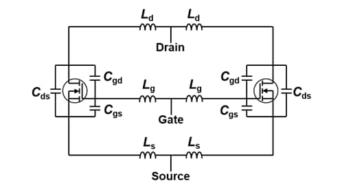
Figure 1. Model equivalent circuit of two MOSFETs connected in parallel 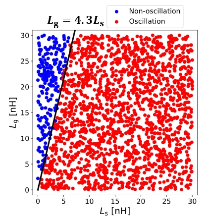
Figure 2. Simulation of oscillation in two MOSFETs with zero gate resistance connected in parallel 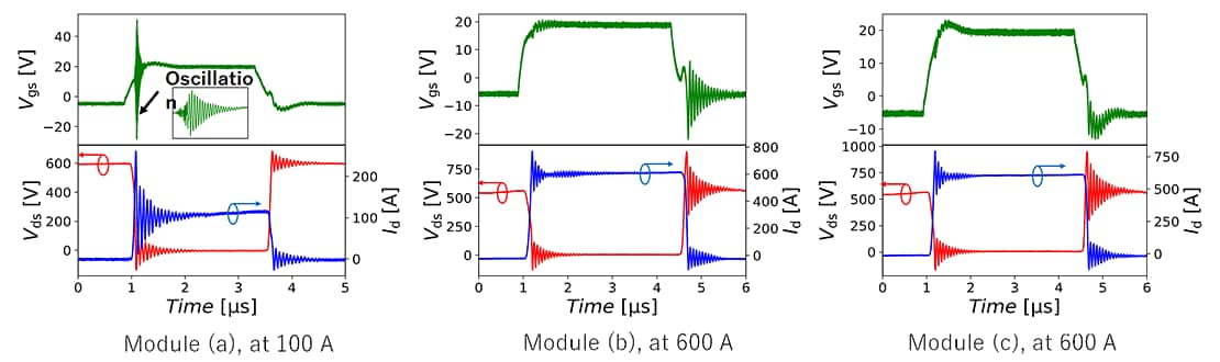
Vgs: Gate-Source voltage, Vds: Drain-Source voltage, Id: Drain current
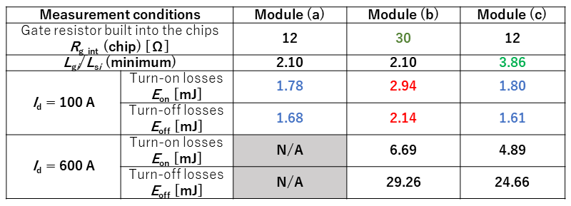
Figure 3. Switching waveforms and switching losses of the prototype modules (Source: Toshiba Group tests) Original – Toshiba
-

Toshiba Electronics Europe GmbH added two new 150V N-channel power MOSFET products based upon their latest generation U-MOS X-H Trench process. The TPH1100CQ5 and TPH1400CQ5 devices are designed specifically for use in high-performance switching power supplies, such as those used in data centres and communication base stations as well as other industrial applications.
With a maximum drain-source voltage (VDSS) rating of 150V and drain current (ID) handling 49A (TPH1100CQ5) and 32A (TPH1400CQ5), the new devices feature a maximum drain-source on-resistance RDS(ON).
The new products offer improved reverse recovery characteristics that are critical in synchronous rectification applications. In the case of TPH1400CQ5, the reverse recovery charge (Qrr) is reduced by approximately 73% to 27nC (typ.) and the reverse recovery time (trr) of 36 ns (typ.) is approximately 45% faster compared with Toshiba’s existing TPH1400CQH, which offers the same voltage and RDS(ON).
Used in synchronous rectification applications, the TPH1400CQ5 reduces the power loss of switching power supplies and helps improve efficiency. If the device is used in a circuit that does not operate in reverse recovery mode, the power loss is equivalent to that of the TPH1400CQH.
When used in a circuit that operates in reverse recovery mode, the new products reduce spike voltages generated during switching, helping to improve EMI characteristics of designs, and reducing the need for external filtering. The devices are housed in a versatile, surface-mount SOP Advance(N) package measuring just 4.9mm x 6.1mm x 1.0mm.
To support designers, Toshiba has developed a G0 SPICE model for rapid verification of the circuit function as well as highly accurate G2 SPICE models, for accurate reproduction of transient characteristics.
Shipments of the new devices start today, and Toshiba will continue to expand their lineup of power MOSFETs that help improve equipment efficiency.
Original – Toshiba
-

Toshiba Electronic Devices & Storage Corporation launched 650V N-channel power MOSFETs “TK068N65Z5, TK095E65Z5, TK095A65Z5, TK095V65Z5, TK115E65Z5, TK115A65Z5, TK115V65Z5 and TK115N65Z5” and added them to the lineup of Toshiba’s latest-generation DTMOSVI series with high-speed diodes (DTMOSVI (HSD)) that uses super junction structure and is suitable for high-efficiency switching power supplies for data centers and power conditioners for photovoltaic generators. Packages of the new products are TO-247, TO-220SIS, TO-220 and DFN8×8.
The new products with the DTMOSVI (HSD) process use high-speed diodes to improve the reverse recovery characteristics important for bridge circuit and inverter circuit applications. Against Toshiba’s existing product TK090A65Z of the standard type DTMOSVI, the new product TK095A65Z5 achieves an approximately 65% reduction in reverse recovery time (trr), and an approximately 88% reduction in reverse recovery charge (Qrr) (measurement conditions: -dIDR/dt=100A/μs).
In addition, the DTMOSVI (HSD) process improves on the reverse recovery characteristics of Toshiba’s existing products DTMOSIV series with high-speed diodes (DTMOSIV (HSD)), and has a lower drain cut-off current at high temperatures. Furthermore, the figure of merit “drain-source On-resistance × gate-drain charge” is also lower.
The high temperature drain cut-off current of the new product TK095A65Z5 is approximately 91% lower, and the drain-source On-resistance × gate-drain charge approximately 70% lower, than in Toshiba’s existing product TK35A65W5. This advance will cut equipment power loss and help to improve efficiency.
A reference design, “1.6kW Server Power Supply (Upgraded)“, that uses the same series product TK095N65Z5 is available on Toshiba’s website.
Toshiba also offers tools that support circuit design for switching power supplies. Alongside the G0 SPICE model, which verifies circuit function in a short time, highly accurate G2 SPICE models that accurately reproduce transient characteristics are now available.
Toshiba also will continue to expand its lineup of the DTMOSVI series. This will enhance switching power supply efficiency, contributing to energy-saving equipment.
Applications
Industrial equipment
- Switching power supplies (data center servers, communications equipment, etc.)
- EV charging stations
- Power conditioners for photovoltaic generators
- Uninterruptible power systems
Features
- MOSFETs with high-speed diodes in the latest-generation DTMOSVI series
- Reverse recovery time due to high-speed diodes:
TK068N65Z5 trr=135ns (typ.)
TK095E65Z5, TK095A65Z5, TK095V65Z5 trr=115ns (typ.)
TK115E65Z5, TK115A65Z5, TK115V65Z5, TK115N65Z5 trr=110ns (typ.) - High-speed switching time due to low gate-drain charge:
TK068N65Z5 Qgd=22nC (typ.)
TK095E65Z5, TK095A65Z5, TK095V65Z5 Qgd=17nC (typ.)
TK115E65Z5, TK115A65Z5, TK115V65Z5, TK115N65Z5 Qgd=14nC (typ.)
Original – Toshiba
-

Toshiba Electronic Devices & Storage Corporation announced new board of directors and the company’s auditors, with an effective date of June 27, 2024. The composition of the Board of Directors and the company’s Auditors, as of June 27, 2024, will be as follows.
Directors and Officers of the Company
Director, President & CEO – Taro SHIMADA (Toshiba Corporation)
Director, Vice President – Noriyasu KURIHARA
Director – Shin KUROSAWA
Director – Hiroyuki SHINKI (Toshiba Corporation)
Director – Masazumi TOMISHIGE (Toshiba Corporation)
Director – Takanori NAKAZAWA (Toshiba Corporation)
Auditor – Hiroki OKADA
Auditor – Shigeki SUGIMOTO (new nominee)
Auditor – Jun TSUJIMOTO (new nominee)Retiring Directors and Auditors as of June 27, 2024
Seiichi MORI
Yutaka SATA (Toshiba Corporation)
Masami TAKAOKA
Akira NAKANISHI (Toshiba Corporation)Original – Toshiba
-
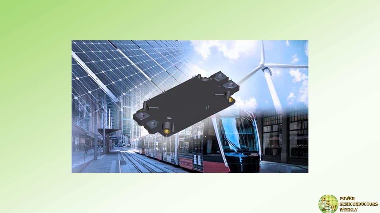
Toshiba Electronic Devices & Storage Corporation has started mass production of a 3rd generation silicon carbide (SiC) 1200 V and drain current (DC) rating 400 A of SiC MOSFET module “MG400Q2YMS3” for industrial equipment and has expanded its lineup.
The new product MG400Q2YMS3 offers low conduction loss with low drain-source on-voltage (sense) of 0.9 V (typ.). It also offers low switching loss with both turn-on switching loss and turn-off switching loss of 13 mJ (typ.). These help to reduce power loss of equipment and the size of cooling device.
MG400Q2YMS3 has a low stray inductance of 12 nH (typ.) and is capable of high-speed switching. In addition, it suppresses surge voltage in switching operation. Thus, it is available for high frequency isolated DC-DC converter.
Toshiba’s SiC MOSFET module of 2-153A1A package has a lineup of five existing products, MG250YD2YMS3 (2200 V / 250 A), MG400V2YMS3 (1700 V / 400 A), MG250V2YMS3 (1700 V / 250 A), and MG600Q2YMS3 (1200 V / 600 A), including new products. This provides a wider range of product selection.
Toshiba will continue to meet the needs for high efficiency and the downsizing of industrial equipment.
Applications
Industrial equipment
- Auxiliary power supply for railway vehicles
- Renewable energy power generation systems
- Motor control equipment for industrial equipment
- High frequency DC-DC converters, etc.
Features
- Low drain-source on-voltage (sense):
VDS(on)sense=0.9 V (typ.) (ID=400 A, VGS=+20 V, Tch=25 °C) - Low turn-on switching loss:
Eon=13 mJ (typ.) (VDD=600 V, ID=400 A, Tch=150 °C) - Low turn-off switching loss:
Eoff=13 mJ (typ.) (VDD=600 V, ID=400 A, Tch=150 °C) - Low stray inductance:
LsPN=12 nH (typ.)
Original – Toshiba
-
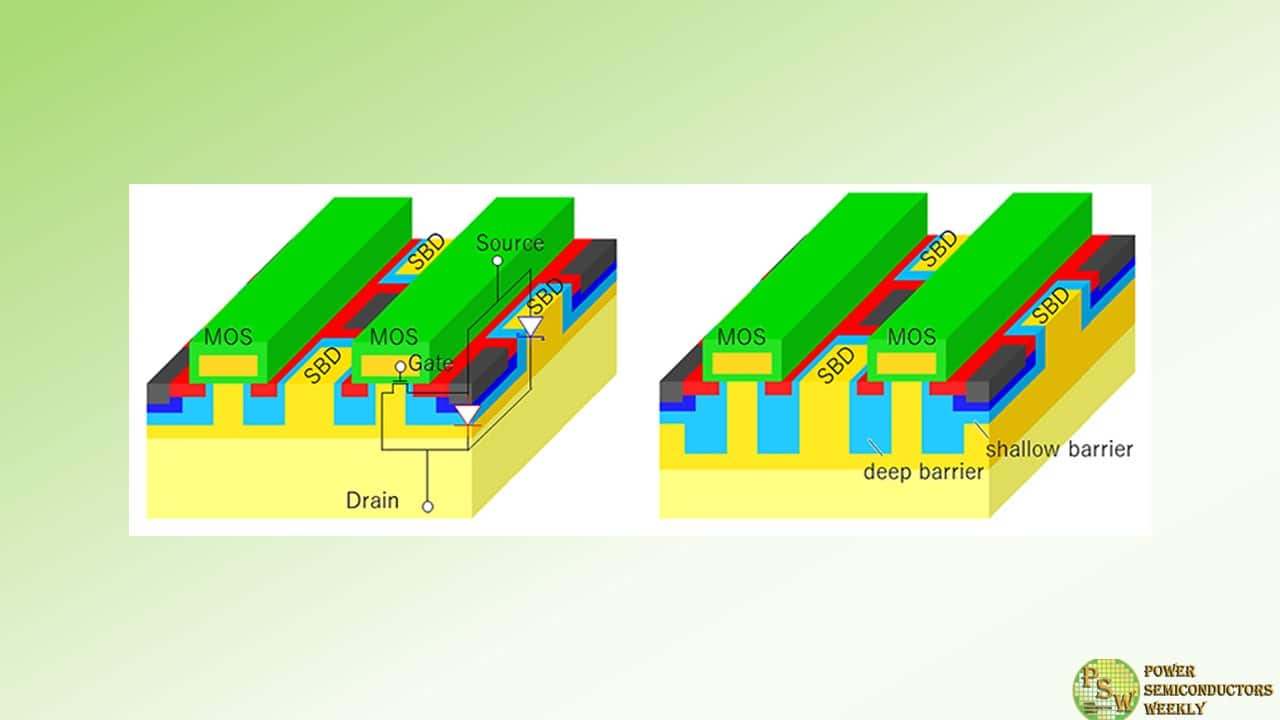
Toshiba Electronic Devices & Storage Corporation has developed a Schottky barrier diode (SBD) embedded metal oxide semiconductor field effect transistor (MOSFET), a significant improvement over the current device structure, while maintaining high reliability and short-circuit ruggedness.
A successful design modification introduces a barrier structure with varying depths in the device structure that maintains the reliability of the reverse conduction operation, the function of an integrated SBD, while suppressing the current leakage from the SBD part that causes destruction during short-circuiting. By making use of new design technology and optimizing the device structure, the new MOSFET achieves lower on-resistance (RonA), with about a 26% improvement over the current structure.
Power semiconductors play a central role in electricity supply and control. They cut energy consumption in all kinds of electronic equipment, and are an important tool for the realization of carbon neutrality. Continued demand expansion is expected from vehicle electrification and the miniaturization of industrial equipment.
Against this background, SiC MOSFETs are seen as next-generation power semiconductors. They deliver better power energy conversion efficiency than Si MOSFETs, and their use has expanded rapidly in recent years. However, SiC MOSFETs have a reliability problem: increased RonA due to reverse conduction operation. Toshiba has now developed an SBD-embedded SiC MOSFET that operates in reverse conduction without increasing RonA.
Reducing the RonA of SiC MOSFET simultaneously causes excess current flow through the MOSFET part during short-circuit operation, reducing the durability of short-circuit operation. However, enhancing the conduction of the embedded SBD to improve the reliability of reverse conduction operation increases its current leakage during short-circuit operation, which also decreases the durability of short-circuit operation.
Introducing a deep barrier structure can suppress both the excess current of the MOSFET and SBD current leakage during short-circuit operation, but it also obstructs current flow from the SBD, raising concerns about decreased reliability in diode conduction.
This led Toshiba to consider a barrier structure divided into shallow and deep areas. The deep barrier area successfully suppresses excess current from the MOSFET part during short-circuit operation, and reduces SBD current leakage, while leaving a shallow area effectively spreads current from the SBD without any obstruction by the barrier.
This improves ruggedness during short-circuit operation while maintaining excellent reliability in reverse conduction operation. Toshiba has provided some customers with test samples of SiC MOSFETs with embedded SBD that apply the new technology since December 2023 for evaluation, toward further enhancing performance.
By making use of its new design technology and optimizing the device structure, Toshiba has developed a prototype 1.2 kV class SBD-integrated MOSFET. This achieves a low RonA of 2.0 mΩcm2, about a 26% improvement over the current structure. Toshiba will present the details of this technology at The 36th International Symposium on Power Semiconductor Devices and ICs (ISPSD) 2024, an international conference on power semiconductors, which is being held in Bremen, Germany from June 2 to 6.
Original – Toshiba
-
Toshiba Electronics Europe GmbH and Toshiba Materials CO., LTD. will bring solutions that support customers’ goals in reducing their CO2 footprint at the PCIM 2024 conference and exhibition (Nuremberg 11th – 13th June).
This year, the company will use the event to showcase a combination of several business units that support development of sustainable solutions. Semiconductor, battery, and fine ceramic material solutions form a complete chain of products in key applications from e-mobility, industrial, energy and infrastructure sectors.
Toshiba has manufactured top-class ceramics since the 1970s, and its pioneering Silicon Nitride substrates will be on display along with bearing balls, AMOBEADS™, and Nanocrystalline common mode choke cores.
In Toshiba’s eMobility booth area, visitors will discover demonstrations of automotive thermal management by heat pumps and fans utilising Toshiba’s newly released SmartMCD.
Toshiba’s industrial demonstrations highlight the entire product chain from control to isolation to power conversion stages, incorporating the latest generations of SiC, GaN and low-voltage MOSFET technologies. They include reference design implementations utilising modern topologies for factory automation, power supplies, and motor control applications.
Energy and infrastructure demonstrations will focus on high-power solutions such as IEGT and SiC Modules supporting voltages from 1.2kV to 3.3kV. Toshiba’s SiC Cube illustrates a solution implementation for charging infrastructure utilising SiC MOSFET devices, whereas SCiB batteries demonstrate their effective use for energy storage.
Toshiba representatives are also scheduled to participate in the conference program speeches and poster sessions on Wide Bandgap, power semiconductors and gate driver ICs topics.
Original – Toshiba
-
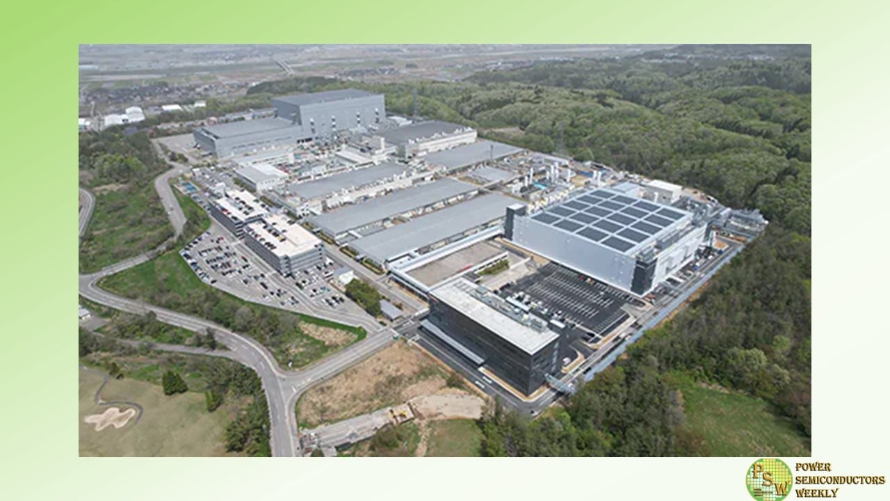
Toshiba Electronic Devices & Storage Corporation held a ceremony to mark the completion of a new 300-millimeter wafer fabrication facility for power semiconductors and an office building at Kaga Toshiba Electronics Corporation in Ishikawa Prefecture, Japan, one of Toshiba’s key group companies. The completion of construction is a major milestone for Phase 1 of Toshiba’s multi-year investment program.
Toshiba will now proceed with equipment installation, toward starting mass production in the second half of fiscal year 2024. Once Phase 1 reaches full-scale operation, Toshiba’s production capacity for power semiconductors, mainly MOSFETs and IGBTs, will be 2.5 times that of fiscal 2021, when the investment plan was made. Decisions on the construction and start of operation of Phase 2 will reflect market trends.
The new manufacturing building follows and will make a major contribution to Toshiba’s Business Continuity Plan (BCP): it has a seismic isolation structure that absorbs earthquake shock and redundant power sources. Energy from renewable source and solar panels on the roof of the building (onsite PPA model) will allow the facility to meet 100% of its power requirement with renewable energy.
Product quality and production efficiency will be boosted by the use of artificial intelligence (AI). Toshiba expects to receive a grant from the Ministry of Economy, Trade and Industry of Japan to subsidize its investment in part of the manufacturing equipment.Power semiconductors play a crucial role in electricity supply and control, and are essential devices for energy efficiency in all electrical equipment. With the continuing electrification of automobiles and the automation of industrial machinery, they are expected to see continued robust demand growth. Toshiba started power semiconductor production on a new 300-millimeter wafer line in the second half of fiscal 2022 at Kaga Toshiba Electronics’ existing facility. Going forward, the company will expand production with the new fab and further contribute to carbon neutrality.
Overview of Kaga Toshiba Electronics Corporation
Location: 1-1, Iwauchi-machi, Nomi-shi, Ishikawa Prefecture, Japan
Established: December, 1984
President and Representative Director: Satoshi Aida
Employees: 1,150 (as of March 31, 2024)
Main Products: Discrete semiconductors (power semiconductors, small-signal devices and optoelectronic devices)
Web: Kaga Toshiba Electronics CorporationOriginal – Toshiba
-

Toshiba Electronic Devices & Storage Corporation announced new board of directors, with an effective date of June 1, 2024. The composition of the Board of Directors and the company’s Auditors, as of June 1, 2024, will be as follows:
Directors and Officers of the Company:
- Director, President & CEO – Taro SHIMADA (Toshiba Corporation)
- Director, Vice President – Noriyasu KURIHARA
- Director – Seiichi MORI
- Director – Shin KUROSAWA
- Director – Hiroyuki SHINKI (Toshiba Corporation)
- Director – Masazumi TOMISHIGE (Toshiba Corporation)
- Director – Takanori NAKAZAWA (Toshiba Corporation)
- Director – Yutaka SATA (Toshiba Corporation)
- Auditor – Hiroki OKADA
- Auditor – Masami TAKAOKA
- Auditor – Akira NAKANISHI (Toshiba Corporation)
Retiring Directors as of June 1, 2023:
- Norifumi INUKUBO
- Hiroshi KURIKI
Original – Toshiba
-
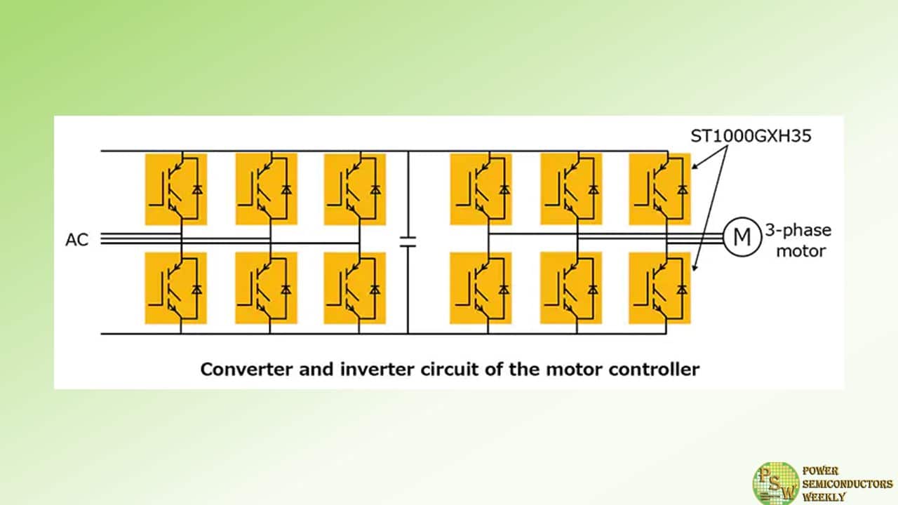
Toshiba Electronic Devices & Storage Corporation has launched a newly developed press pack IEGT “ST1000GXH35” with ratings of 4500 V/1000 A for use in high-voltage converters such as DC power transmission systems and industrial motor controllers.
The new product ST1000GXH35 employs trench-type IEGT chips and high-speed diode chips. The IEGT chips reduce collector-emitter saturation-voltage and improve shutdown tolerance, short-circuit tolerance, and high-temperature tolerance. Therefore, collector-emitter saturation-voltage (VCE(sat) ) has been reduced by approximately 28 % from 3.00 V to 2.15 V (typical) compared with the existing product ST750GXH24.
The high-speed diode chips suppress voltage oscillation during reverse recovery and improve reverse recovery tolerance and high-temperature tolerance. The new product can be used at a higher turn-on speed than the existing product, therefore the turn-on switching loss (Eon) has been reduced by approximately 34 % from 4.15 J to 2.75 J (typical).
Furthermore, the test voltage for shutdown tests and short-circuit tests has been enhanced to 3400 V in response to applications requiring high voltage. In addition, the junction temperature rating has been increased from 125 °C to 150 °C (maximum) by improving the high-temperature tolerance of the diode.
ST1000GXH35 contributes to size reduction and high output for high-voltage converters such as DC power transmissions, static VAR compensators, and industrial motor controllers.
Applications
- DC power transmissions
- Static VAR compensators
- Industrial motor controllers
Features
- Low collector-emitter saturation voltage and low turn-on switching loss
- Enhanced to test-voltage 3400 V for shutdown and short-circuit tests
- Maximum junction temperature rating: Tj(max)=150 °C
Original – Toshiba
