-

Toshiba Electronic Devices & Storage Corporation will move its semiconductor business unit and its research and development (R&D) center to a new building in Toshiba Corp’s Komukai Complex in Kawasaki. It will also be home to Toshiba’s Corporate R&D Center, strengthening synergy within Toshiba Group’s R&D organizations.
The new building will provide spaces for exhibitions and other events open to people from outside the company, as well as collaboration spaces for co-creation with customers. It will create an environment customers can feel free to visit, and promote new ways of working unconstrained by typical workplace limitations.
Virtually all energy will be derived from renewable, and CO2 emissions from power consumption will target zero, contributing to the realization of carbon neutrality.
Division names: Semiconductor Division and Electronic Devices & Storage R&D Center
Address: 1, Komukai-Toshiba-cho, Saiwai-ku, Kawasaki, Kanagawa 212-8583, Japan
Phone number: +81-44-548-2000 (switchboard; no change)
Relocation date: January 22, 2024The address of the Storage Products Division and the company’s registered address remain unchanged, as below.
Storage Products Division
8, Shinsugita-cho, Isogo-ku, Yokohama, Kanagawa 235-8522, JapanRegistered headquarters
1-1, Shibaura 1-Chome, Minato-ku, Tokyo, JapanOriginal – Toshiba
-
STMicroelectronics has signed a long-term silicon carbide (SiC) supply agreement with Li Auto, a leader in China’s new energy vehicle market that designs, develops, manufactures, and sells smart premium electric vehicles. Under this agreement, STMicroelectronics will provide Li Auto with SiC MOSFET devices to support Li Auto’s strategy around high-voltage battery electric vehicles (BEVs) in various market segments.
As the automotive industry transforms towards electrification and decarbonization, high-voltage BEVs have become a popular choice for car makers. These vehicles offer outstanding energy efficiency and extended mileage. Li Auto, known for its extended-range electric vehicles (EREVs), is entering the BEV market with its first-ever high-tech flagship family MPV BEV model premiered in Q4 2023. With plans to introduce more high-voltage BEV models soon, Li Auto will require high volumes of SiC MOSFETs that it will integrate into its traction inverters to ensure superior electric-vehicle performance.
ST’s SiC devices increase performance and efficiency through higher switching frequencies, breakdown voltages, and thermal resistance. These are all particularly critical characteristics at the higher operating voltages required for battery electric vehicles. Li Auto is adopting ST’s advanced third-generation 1200V SiC MOSFET in the traction inverter of its upcoming 800V BEV platform, to ensure industry-leading process stability and performance, efficiency, and reliability.
“Li Auto is committed to providing families with premium EVs exceeding their expectation. This agreement with ST stands as a testament to Li Auto’s unwavering dedication in BEV product development. Collaborating with the renowned global leader in SiC technologies, we anticipate a forthcoming relationship filled with innovation and success,” said Qingpeng MENG, Vice President of Supply Chain, Li Auto.
Holding more than 50% market share in SiC MOSFETs worldwide, ST’s SiC technology has earned high praise from top OEMs for its electric-vehicle performance. It is widely used in onboard chargers and power modules.
“As a world leader in power devices and wide bandgap semiconductor technologies, ST has established long-term supply agreements with major car makers and Tier 1 suppliers. The SiC supply agreement with Li Auto marks a significant step building upon our existing long-term relationship in other automotive applications,” said Henry CAO, Executive Vice President of Sales & Marketing, China Region, STMicroelectronics. “ST is committed to supporting Li Auto’s ambition to become a top premium electric vehicle brand in China, offering their customers superior vehicle performance and range with our innovative SiC technologies.”
Original – STMicroelectronics
-
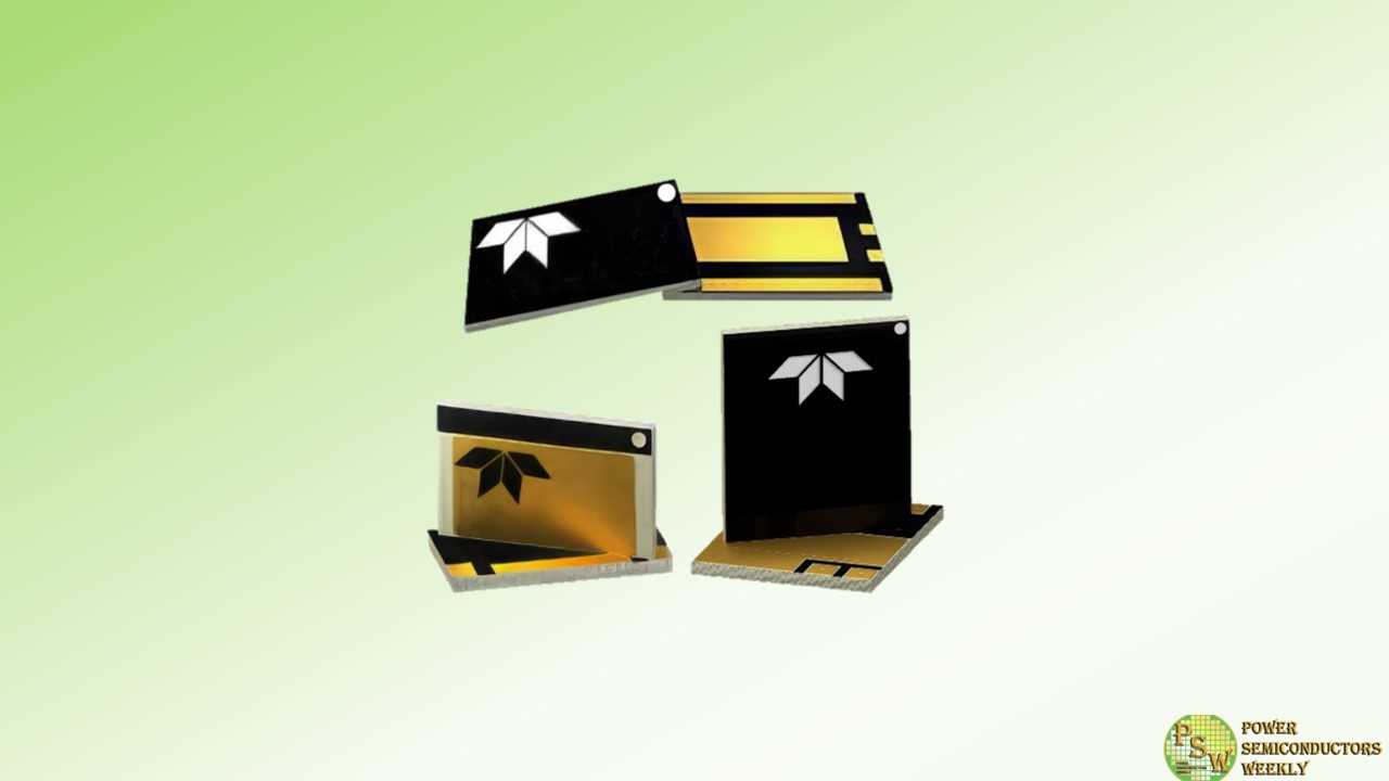
Teledyne e2v HiRel announced the addition of new space screened versions of its popular 100 V, 90 A and 650 V, 30 A high reliability gallium nitride high electron mobility transistors (GaN HEMTs).
- TDG650E30BSP
- TDG100E90BSP
- TDG100E90TSP
The new parts go through NASA Level 1 or ESA Class 1 screening flow and can be brought up to full Level 1 conformance with extra qualification testing if desired. Typical applications include battery management, dc-dc converters, and space motor drives.
Two new 100 V parts are available with both bottom-side and top-side cooled packaging. One new 650 V 30 A GaN-on-Silicon power transistor is available in a bottom-side cooled package. Each device is available with options for EAR99 or European sourcing.
Teledyne e2v HiRel’s GaN HEMTs feature single wafer lot traceability, extended temperature performance from -55 to +125°C, and low inductance, low thermal resistance packaging.
“Our customers have embraced the previous release of 650 V space screened devices, and we have expanded our portfolio to provide additional options. These GaN HEMT products save customers time and money by providing standard devices without the need for additional screening.” said Mont Taylor, VP of Business Development for Teledyne e2v HiRel. “Our expanded catalog with standard burn-in make it easy for designers to utilize the latest in GaN in their designs.”
Gallium nitride devices have revolutionized power conversion in other industries and are now available in radiation tolerant, plastic encapsulated options that have undergone stringent reliability and electrical testing to help ensure mission critical success. The release of these new GaN HEMTs delivers to customers the efficiency, size, and power-density benefits required in critical aerospace and defense power applications.
Original – Teledyne e2v HiRel
-
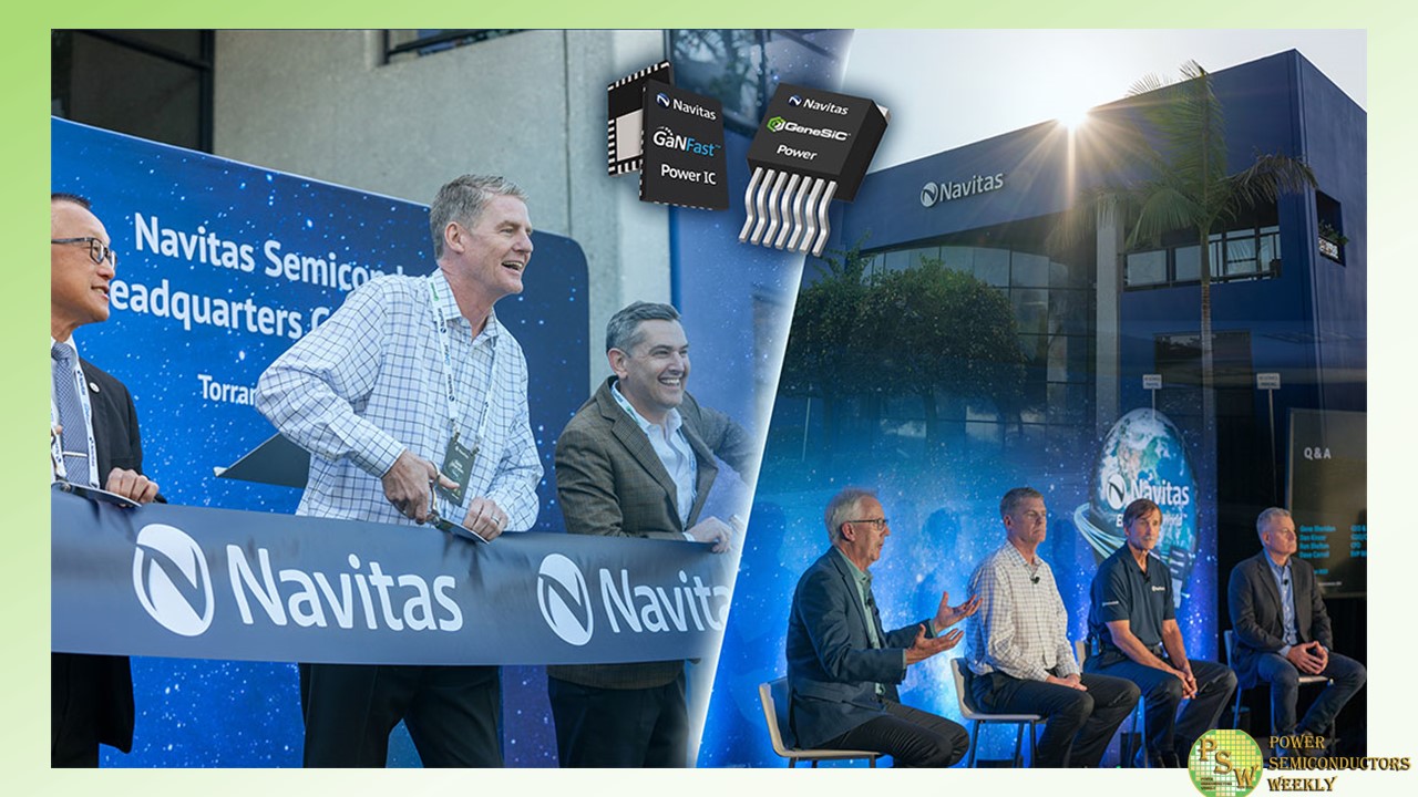
Navitas Semiconductor held an Opening Ceremony and 2023 Investor Day at its new headquarters in Torrance, CA.
Torrance Mayor, George Chen, and Dustin McDonald from the Office of the Governor of California joined Navitas’ CEO and co-founder Gene Sheridan to speak and cut the ribbon, officially opening Navitas’ new headquarters. Around 100 highly-skilled Navitas staff are employed in Torrance for all aspects of GaN and SiC design, applications, test, characterization and quality plus finance, marketing and HR. Further team growth is planned for 2024, including a $20M investment to add SiC epi-growth capability for strategic manufacturing expansion.
The well-attended investor meeting began with Mr. Sheridan’s recap on a year of significant growth for Navitas, with a doubling of revenue, a $92M capital raise, four major new technology platforms and an update on Navitas’ mission to ‘Electrify Our World™. Then, Mr. Sheridan outlined a $1.3T electrification market opportunity as GaN and SiC enable and accelerate our transition away from fossil fuels to a carbon-neutral, full-electrified world, envisaged as ‘Planet Navitas’.
Dan Kinzer, co-founder and COO/CTO then introduced technology platforms including Gen-4 GaNSense half-bridges for motor drive and mobile fast chargers, GaNSafe – the world’s most protected GaN powertrain, GaNSense Control, and a revolutionary new bi-directional GaN power IC platform with up to 9x smaller chip size than legacy silicon MOSFETs or IGBTs. Sid Sundaresan, SVP for the GeneSiC product line added more detail on the Gen-3 Fast SiC platform.
In May, Navitas announced a qualified customer pipeline of $760M, across mobile, solar/ESS, EV/eMobility, data center and appliance/industrial markets. At the Investor Day, David Carroll, SVP Worldwide Sales announce that the pipeline had increased by 65% to $1.25B, with 10/10 top mobile OEMs and majority of solar inverter makers. Investors also heard from the voices of Navitas customers, including Rick Liu from Accopower for EV, Belkin’s Steve Malony for mobile, Philipp Guo from VREMT for EV, Adam Weissman from Anker for mobile, and Harron Inam from DG Matrix for EV roadside charging.
Ron Shelton, Navitas CFO, presented more detail on the impressive financial results with increased gross margin, and over $170M is cash and no debt, plus a long-term target to grow 6x-10x more than the market, with 50%+ gross margins.
In-person visitors then toured the Navitas facility, including past & present demos and the ‘Electrify Studio’ experience – where Navitas is creating a vision for our electrified planet – plus SiC design, GaN IC design, applications, test & characterization, quality & reliability.
The day concluded with a celebration at the Crypto.com Arena, where guests enjoyed the LA Clippers’ victory—a fitting finale to a day filled with inspiration, innovation, and collaboration.
Comprehensive Investor Day material is available via the Navitas website, with presentation slides, and complete video playback of the main presentations, customer testimonials, and facility tour.
Original – Navitas Semiconductor
-

Due to the positive development of the market capitalization, the Siltronic share is rejoining the MDAX index today. After several months in the SDAX, the Siltronic AG share is once again represented in the second most important index of the German stock exchange. Additionally, Siltronic shares will remain part of the TecDAX.
Throughout the year, Siltronic’s share price was negatively impacted by the market weakness in the semiconductor industry, which led to its descent to the SDAX in June 2023. Since then, the share price has steadily recovered, and the company’s market capitalization has increased significantly.
Dr. Michael Heckmeier, CEO of Siltronic, commented on this development: “The re-inclusion of Siltronic in the MDAX reflects investors’ confidence in our future prospects and our continued growth. This underscores the robust share price performance of recent months.”
Siltronic’s inclusion in the MDAX is part of Deutsche Börse AG’s regular quarterly review. The decision is based on the market capitalization of the freely tradable shares, i.e. the free float market capitalization.
Original – Siltronic
-

Infineon Technologies AG announced its commitment to set a science-based target. By that Infineon expands its climate strategy even further. The company is very well on track towards CO2-neutrality by 2030, relating to its direct and indirect energy related emissions (Scope 1 and 2).
After having already reduced these emissions by 56.8 percent to date versus the base year of 2019, Infineon now sets itself even more ambitious targets by involving the supply chain (Scope 3) in the company’s climate protection efforts.
“Decarbonization is a guiding principle for Infineon. We have made great progress. With our commitment to set a science-based target, we are taking the next important step, adhering to the widely respected global standard for tackling climate change”, said Elke Reichart, Chief Digital Transformation Officer and responsible for Sustainability at Infineon. “We are actively inviting our suppliers to join us on our journey by setting their own carbon reduction targets. To truly address climate change, collaboration across the entire value chain, transparent and comprehensive data as well as global standards are foundational.”
Infineon has doubled its revenue since 2019 and halved its CO2 emissions (Scope 1 and 2) at the same time. The main drivers for lowering emissions are energy efficiency measures, comprehensive PFC abatement measures and switching its operations to renewable energy, which makes proportionally the largest contribution.
In 2023, Infineon reaches another key milestone in this respect. The two largest manufacturing sites in Asia – Kulim and Melaka in Malaysia – have now transitioned to green electricity, following the switch to renewables at its European and North American sites in 2021 and 2022 respectively.
The Science Based Targets initiative (SBTi) serves as a benchmark for ambitious climate action in the private sector. The initiative provides a clearly defined pathway for companies to reduce greenhouse gas (GHG) emissions. Targets are considered ‘science-based’ if they are in line with the latest climate science in order to meet the goals of the Paris Agreement – limiting global warming to well below 2°C above pre-industrial levels and pursuing efforts to limit warming to 1.5°C. SBTi is a partnership between the Carbon Disclosure Project (CDP), the United Nations Global Compact, World Resources Institute (WRI) and the World Wide Fund for Nature (WWF).
In 2020, Infineon had set its carbon neutrality target 2030 (Scope 1 and 2 emissions) already in line with science-based target requirements. With the expansion of its climate strategy to include Scope 3, Infineon is working closely together with supply chain partners and is putting special emphasis on further improvements in data availability and accuracy.
Original – Infineon Technologies
-
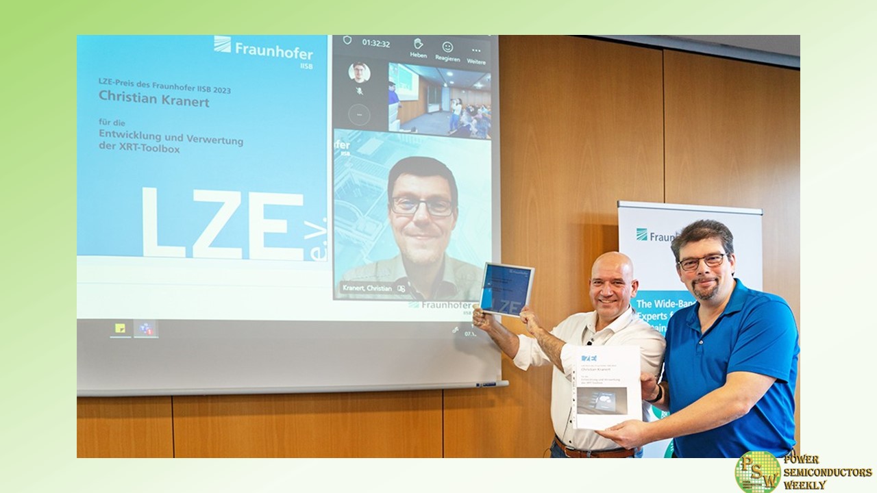
Dr. Christian Kranert, Group Manager Equipment and Defect Simulation of the Materials Department at Fraunhofer IISB, developed a new software for the fast, full-wafer and automated detection and classification of crystal defects in silicon carbide (SiC) substrates. He also pushed the licensing of his new, so-called x-ray ropography (XRT) toolbox to the users of the x-ray topography measuring device XRTmicron from Rigaku. Another highlight is the establishment of two new SEMI International Standards for 4H-SiC defect quantification using XRT test methods.
These outstanding results confirm the success of the Joint Labs model at Fraunhofer IISB. Joint Labs are an exclusive opportunity to collaborate with Fraunhofer IISB in an industry-compatible laboratory environment.
Rigaku Europe SE and Fraunhofer IISB are operating the Center of Expertise for X-ray Topography, a joint lab that is located at the IISB’s headquarters in Erlangen, Germany. This fruitful collaboration is vividly illustrated by the new business in the field of SiC wafer mapping, which Rigaku has built up around its XRTmicron product line in less than two years.
The new LZE Prize honors Fraunhofer IISB employees for exceptional achievements. The LZE Prize is awarded for outstanding acquisitions or particularly successful collaborations, new networks with domestic and foreign partners or above-average achievements in the transfer of know-how from research to industry. The Leistungszentrum Elektroniksysteme (LZE) is a joint initiative of the Fraunhofer-Gesellschaft, Fraunhofer IIS, Fraunhofer IISB, and FAU Erlangen-Nürnberg (FAU), together with industry partners and further research institutes.
Original – Fraunhofer IISB
-
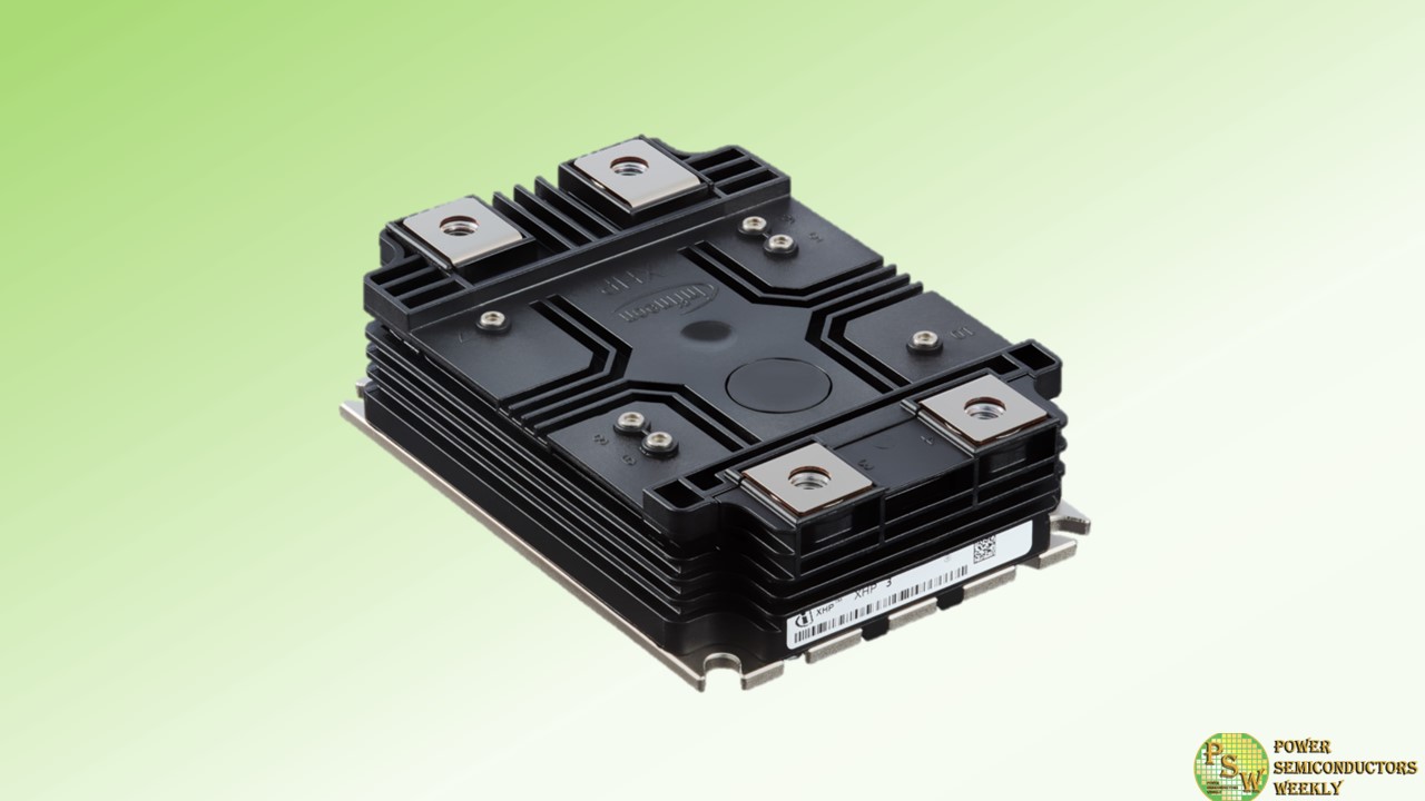
The paradigm shift towards offloading complexity to suppliers and adopting smaller IGBT modules is evident in various applications. In response to the global push for downsizing and integration, Infineon Technologies AG introduced the 4.5 kV XHP™ 3 IGBT modules that will fundamentally change the landscape for medium voltage drives (MVD) and transportation applications operating at 2000 to 3300 V AC in 2- and 3-level topologies.
Applications benefiting from the new devices include large conveyor belts, pumps, high-speed trains, locomotives, as well as commercial, construction and agricultural vehicles (CAV).
The XHP family comprises a 450 A dual IGBT module with TRENCHSTOP™ IGBT4 and an emitter-controlled diode, and a 450 A double diode module with emitter-controlled E4 Diode. Both modules feature improved isolation of 10.4 kV. Together, they help to simplify paralleling and downsizing without sacrificing efficiency.
Previously, complex busbars were required to parallelize switching modules, resulting in complicated design efforts and leakage inductance. The innovative design of the XHP family simplifies paralleling by conveniently placing the connections side by side. As a result, only a single straight busbar is required for paralleling.
The 4.5 kV XHP family also allows developers to reduce the number of units. Conventional IGBT solutions use multiple single switches and a double diode. With the new devices, however, designs can be reduced to two dual switches and a smaller double diode – a significant step forward in integrated drives.
The combination of the XHP 3 FF450R45T3E4_B5 dual switch and the DD450S45T3E4_B5 double diode enables significant cost savings and a smaller footprint. For example, Infineon’s previous IGBT solutions required four 140 x 190 mm² or 140 x 130 mm² switches and one 140 x 130 mm² double diode. With the new XHP family, the components can be reduced to two 140 x 100 mm² dual switches and a smaller 140 x 100 mm² double diode.
The IGBT modules FF450R45T3E4_B5 and DD450S45T3E4_B5 are available now. More information is available at www.infineon.com/XHP.
Original – Infineon Technologies
-

Toshiba Electronic Devices & Storage Corporation announced new board of directors, with an effective date of December 22, 2023.
The composition of the Board of Directors and the company’s Auditors, as of December 22, 2023, will be as follows:
Directors and Officers of the Company
Director, President & CEO Taro Shimada (Toshiba Corporation)
Director, Vice President Noriyasu Kurihara
Director Seiichi Mori
Director Norifumi Inukubo (Toshiba Corporation)
Director Hiroshi Kuriki (Toshiba Corporation)
Director Shin Kurosawa
Director Hiroyuki Shinki (Toshiba Corporation)
Director Yutaka Sata (Toshiba Corporation)
Auditor Hiroki Okada
Auditor Masami Takaoka
Auditor Akira Nakanishi (Toshiba Corporation)Retiring Director as of December 22, 2023
Hiroyuki SatoOriginal – Toshiba
-

Power Integrations announced that it has been Certified™ by Great Place To Work® for a second consecutive year. In a recent anonymous survey, 85 percent of employees said that Power Integrations is a great place to work—28 points higher than the average U.S. company. Additionally, 91 percent reported feeling that they make a difference at the company, while 86 percent said they would strongly endorse the company to friends and family as a great place to work.
Stated Balu Balakrishnan, chairman and CEO of Power Integrations: “We are proud to be recognized once again with Great Place To Work Certification. As an innovation-driven company, our success depends on developing a talented, stable workforce and a culture that promotes creativity and risk-taking. While we will always strive to improve, it is gratifying to learn that so many of our employees are happy and proud to be part of Power Integrations.”
“Great Place To Work Certification is a highly coveted achievement that requires consistent and intentional dedication to the overall employee experience,” says Sarah Lewis-Kulin, vice president of global recognition at Great Place To Work.
She emphasizes that Certification is the sole official recognition earned by the real-time feedback of employees regarding their company culture. “By successfully earning this recognition, it is evident that Power Integrations stands out as one of the top companies to work for, providing a great workplace environment for its employees.”
Power Integrations currently has numerous job openings across North America, Europe and Asia. To learn more, interested job seekers can visit the “Careers” page of the Power Integrations website.
Original – Power Integrations
