-
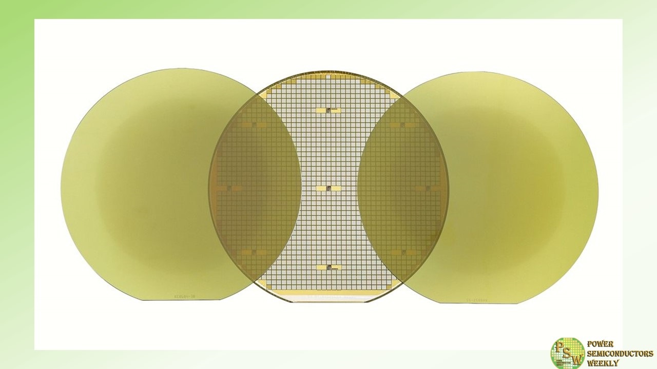
Vitesco Technologies and onsemi announced a 10-year long-term supply agreement worth $1.9 billion (€1.75 billion) for silicon carbide (SiC) products to enable Vitesco Technologies’ ramp in electrification technologies. Vitesco Technologies, a leading international manufacturer of modern drive technologies and electrification solutions, is providing an investment of $250 million (€230 million) to onsemi for new equipment for SiC boule growth, wafer production and epitaxy to secure access to SiC capacity.
The equipment will be used to produce SiC wafers to support Vitesco Technologies’ growing SiC demand. In parallel, onsemi, a leader in intelligent power and sensing technologies, will continue to invest substantially into end-to-end SiC supply chain.
In addition, Vitesco Technologies and onsemi will collaborate on optimized customer solutions for Vitesco Technologies. onsemi’s highly efficient EliteSiC MOSFETs will be used by Vitesco Technologies to execute the recent orders as well as future projects for traction inverters and electric vehicle drives.
SiC semiconductors are a pivotal technology for electrification enabling highly efficient power electronics leading to reduced charging times and longer range for electric cars. Especially at high voltage levels such as 800 V, SiC inverters are more efficient than silicon models. Since 800 V is the prerequisite for fast and thus convenient high-voltage charging, SiC devices are at the beginning of a worldwide boom.
Original – Vitesco Technologies
-
Magnachip Semiconductor Corporation announced that the Company is separating its display and power businesses into separate entities, following approval by its board of directors and strategic review committee.
YJ Kim, Magnachip’s chief executive officer commented, “This strategic separation represents a significant milestone for Magnachip and underscores the Company’s commitment to unlocking long-term value for our shareholders. The internal separation is aimed at enhancing transparency, accountability and flexibility in business. By establishing distinct entities, we believe our investors will be able to better evaluate the financial performance of each business and their respective contributions. Furthermore, this strategic move will allow each entity to allocate its resources, both financial and technical, more effectively to the specific needs of its customers.”
YJ Kim continued, “Magnachip remains dedicated to delivering innovative solutions and exceptional customer experiences in both the display and power sectors, and we are confident that this separation will strengthen our ability to achieve these objectives by enhancing each business’s agility and focus.”
The Company plans to effectuate the internal separation (the “Internal Split-Off”) by establishing a new subsidiary (“NewCo”) under Magnachip Semiconductor, Ltd. (“Magnachip Korea”), the Company’s operating subsidiary. As part of the transaction, all assets and liabilities of the display business will be contributed to NewCo in exchange for equity. Once the Internal Split-Off is completed, Magnachip Korea and NewCo will both be separate operating companies, with NewCo being a wholly owned subsidiary of Magnachip Korea. The Company’s Gumi fabrication facility will remain with Magnachip Korea as an integral part of its power business.
Post-separation, the board of directors of Magnachip will continue to oversee both operating entities, ensuring cohesive governance, while YJ Kim and the executive management team will manage their business and operations. Each of Magnachip Korea and NewCo will remain indirect wholly owned subsidiaries of Magnachip, and the Internal Split-Off is not expected to have any material impact on the Company’s financial reporting or consolidated financial statements.
The Internal Split-Off is expected to be completed in the fourth quarter of 2023.
Original – Magnachip Semiconductor
-

Navitas Semiconductor announced the first in a series of strategic manufacturing investments, to increase control, reduce costs and enhance revenue capacity for its GeneSiC silicon carbide (SiC) power semiconductors.
An initial $20 million investment enables a three-reactor SiC epi-growth facility at the company’s Torrance, CA headquarters. Adding a SiC epitaxial (or “epi”) layer onto a raw SiC wafer is the first step in manufacturing individual SiC power devices. The first AIXTRON G10-SiC epitaxy reactor, with 6” and 8” wafer capability, is expected to be fully qualified and in production in 2024. Navitas views the epi-growth services to be provided by its new facility as a critical process step that could support up to an additional $200 million in annual production. The company expects to continue the use of third-party vendors for additional epi-growth, wafer fabrication and assembly operations.
“We are proud that an important technology innovator such as Navitas chose our new G10-SiC to further accelerate the adoption of SiC in the growing market for energy efficient power devices. This is especially significant as AIXTRON and Navitas are both firm believers and pioneers in the unstoppable advance of GaN and SiC over legacy silicon. It is through partnerships like ours, where highly innovative companies work together, that this important transition can be realized,” says Dr. Felix Grawert, CEO and President of AIXTRON SE.
“Adding a high-quality SiC epi-layer onto a raw SiC wafer is a critical process step prior to individual device manufacturing, and adding the AIXTRON in-house epi capability to existing subcontract process flows expands available capacity, lowers finished wafer cost, increases quality and reduces cycle times”, said Dan Kinzer, Navitas COO / CTO and co-founder. “The development and manufacturing business partnership with Aixtron includes ongoing technical and co-development support.”
Navitas’ investment in internal epi capacity is one of several initiatives in support of the company’s recently-announced $760M customer pipeline of estimated potential future business, based on expressed customer interest for qualified programs. While the conversion of this pipeline into orders or shipments depends on many factors in addition to possessing available capacity, the company expects its epi capacity expansion will provide a favorable return on investment under most anticipated planning scenarios.
Navitas recently completed an $80 million follow-on common stock offering and plans to use proceeds from the offering for strategic manufacturing investments, among other possible uses, including working capital and general corporate purposes.
Original – Navitas Semiconductor
-
Coherent Corp. and Mitsubishi Electric Corporation have signed a memorandum of understanding (MOU) to collaborate on a program to scale manufacturing of SiC power electronics on a 200 mm technology platform.
The market for electric vehicles is expanding worldwide and is just one of several emerging applications driving the exponential growth in SiC power devices, which have lower energy losses, higher operating temperatures, and higher switching speeds compared with power devices based on silicon. The high efficiency of SiC power devices is expected to be a significant contributor to global decarbonization and the green transformation.
To meet the rapidly growing demand, Mitsubishi Electric announced an investment of approximately 260 billion yen in the five-year period ending March 2026. A major portion of the investment, approximately 100 billion yen, will be used to construct a new plant for SiC power devices, based on a 200 mm technology platform, and enhance related production facilities. Under the MOU, Coherent will develop a supply of 200 mm n-type 4H SiC substrates for Mitsubishi Electric’s future SiC power devices manufactured at the new facility.
“We are excited to build on our relationship with Mitsubishi Electric, a pioneer in SiC power devices and a global market leader in SiC power modules for high-speed trains, including the famous Shinkansen in Japan,” said Sohail Khan, Executive Vice President, New Ventures & Wide-Bandgap Electronics Technologies at Coherent. “We have a long track record of supplying SiC substrates to Mitsubishi Electric and are looking forward to expanding our relationship with them to scale their new 200 mm SiC platform.”
“Coherent has been for many years a reliable supplier of high-quality 150 mm SiC wafer substrates to Mitsubishi Electric,” said Masayoshi Takemi, Executive Officer, Group President, Semiconductor & Device at Mitsubishi Electric. “We are delighted to enter into this close partnership with Coherent to scale our respective SiC manufacturing platforms to 200 mm.”
Coherent has decades of experience in the development of SiC materials. The company demonstrated the world’s first 200 mm conductive substrates in 2015. In 2019, Coherent began to supply 200 mm SiC substrates under REACTION, a Horizon 2020 four-year program funded by the European Commission.
Over the years, Mitsubishi Electric has led the SiC power module markets for high-speed trains, high-voltage industrial applications, and home appliances. Mitsubishi Electric made history by launching the world’s first SiC power modules for air conditioners in 2010, and became the first supplier of a full SiC power module for Shinkansen high-speed trains in 2015. Mitsubishi Electric has also built extensive expertise by serving customers’ needs for high performance and high reliability through its outstanding techniques of processing and screening, as well as many other facets of developing and manufacturing SiC power modules.
Power electronics based on SiC have demonstrated their potential to have a highly beneficial impact on the environment via significant reductions in carbon dioxide emissions. Through the rapidly growing demand for SiC power devices, Coherent and Mitsubishi Electric will accelerate their contribution to sustainable energy consumption and the decarbonization of society.
Original – Coherent
-
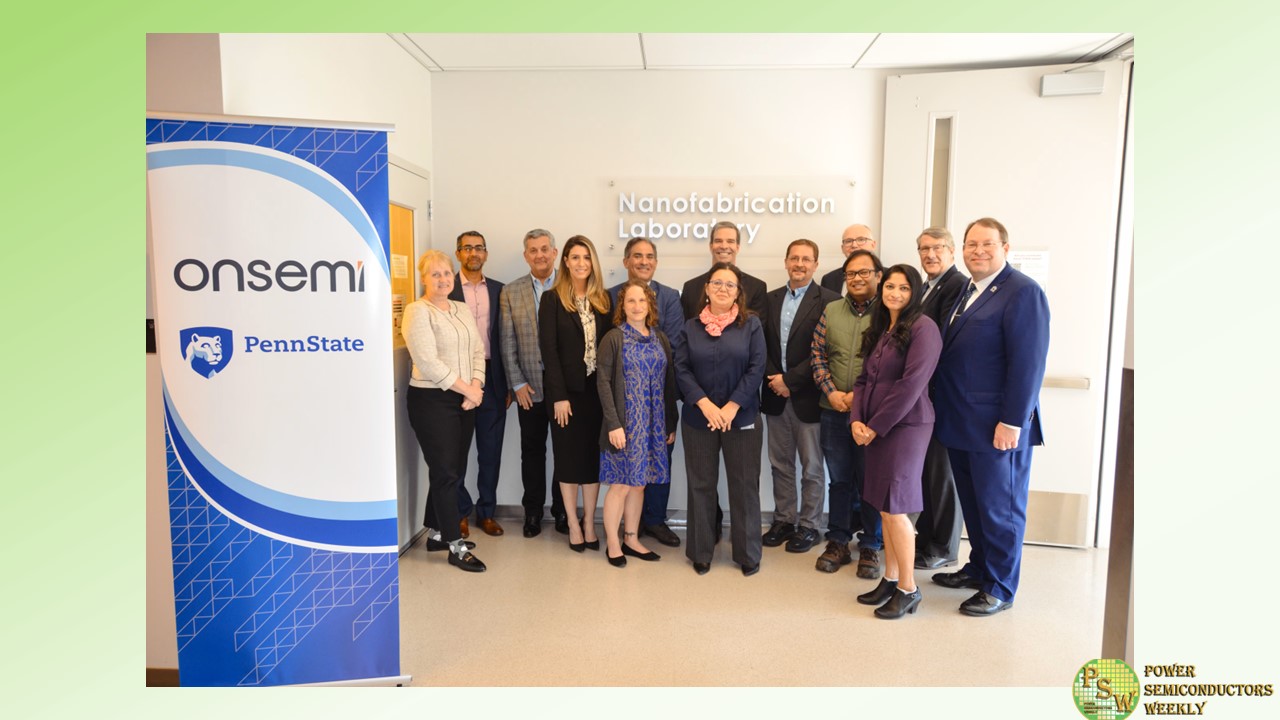
Penn State and onsemi, a leader in intelligent power and sensing technologies, announced the signing of a memorandum of understanding (MOU) towards an $8 million strategic collaboration which includes the establishment of the onsemi Silicon Carbide Crystal Center (SiC3) at Penn State’s Materials Research Institute (MRI). onsemi will fund SiC3 with $800k per year over the next 10 years.
Silicon carbide (SiC) is vital for enabling efficiency in electric vehicles (EVs), EV charging and energy infrastructure and contributes to the decarbonization of the global economy. Academic research in SiC made great advancements in the late 1990s and early 2000s, but has since diminished in the U.S. This agreement will put SiC crystal research in America back on the map.
In addition to conducting SiC research at SiC3, Penn State and onsemi will raise awareness about the increasing demand for tech jobs in the semiconductor industry. This is part of their efforts to enhance the share of U.S. semiconductor manufacturing. They also will partner on workforce development initiatives such as internship and cooperative programs and include SiC and wide bandgap crystal studies in Penn State’s curriculum. The relationship with Penn State is part of onsemi’s commitment to promoting STEAM (Science, Technology, Engineering, Arts, and Mathematics) education, ranging from helping K-12 students in underserved communities to university collaborations that support the development of the workforce for today and the future.
Lora Weiss, Penn State senior vice president of research, noted that the Penn State-onsemi collaboration is a match that makes perfect sense given each entity’s demonstrated strengths.
“onsemi is a proven innovator, delivering a comprehensive portfolio of intelligent power and sensing technologies to enable and accelerate sustainable solutions across multiple markets,” Weiss said. “At the same time, as per the National Science Foundation’s research expenditure rankings, Penn State is ranked first in materials science and second in materials engineering. We have world-class nanofab and characterization facilities that support research on thin films, silicon carbide and other materials used in semiconductors and other technologies. These complementary capabilities between onsemi and Penn State will have a strong impact on research and development, economic growth, and workforce development.”
Penn State’s capabilities make them an ideal academic partner for onsemi to advance the state of the art in silicon crystal growth.
“Penn State is uniquely positioned to rapidly establish a silicon carbide crystal growth research program,” said Pavel Freundlich, chief technology officer, Power Solutions Group, onsemi. “The university offers a wide breadth of capability based on its current materials research, wafer processing capabilities in its nanofab facility, and a comprehensive, world-class suite of metrology instrumentation.”
The relationship developed over a period of due diligence during which it became clear that their cooperative efforts would position Penn State and onsemi as leaders in SiC research.
“Over the next decade, this collaboration will enable Penn State to become the nation’s leading resource for semiconductor crystal science and workforce development,” said Justin Schwartz, Penn State executive vice president and provost. “And this would not be possible without the relationship-building efforts of Priya Baboo, senior director of corporate and industry engagement, and the technical expertise of Joshua Robinson, professor of materials science and engineering, and their counterparts at onsemi.” Scott Allen, vice president, University Relations, onsemi, added that “Penn State’s expansion of its curriculum to offer specialty courses in SiC and wideband gap technology will play a key role in meeting onsemi’s strategic workforce development goals and help to meet American semiconductor workforce goals as outlined in the recently signed CHIPS and Science Act.”
Original – onsemi
-

AIXTRON SE plans to invest up to 100 million euros at its Herzogenrath site. A new innovation center is to be built, which will provide the manufacturer of deposition equipment to the semiconductor industry with enhanced capacities for research and development. AIXTRON received approval for the new project from the company’s Supervisory Board.
The new innovation center will provide 1000m2 of cleanroom space and will be built on the company’s premises in Herzogenrath, Germany. The new building will create further capacities for the next product generations which are already in preparation, as well as for further product developments beyond that.
“With our products, we address the megatrends of digitalization, electromobility and energy efficiency and are experiencing a strong and steadily growing demand. Technical innovations and product developments that precisely address the needs of our customers are the key to our success. And our dynamic environment offers us further growth opportunities,” says Dr. Felix Grawert, CEO of AIXTRON SE. “We are therefore very pleased that the Supervisory Board has approved this project which will enable us to create the foundation for further product developments and for future growth.”
The importance of product development in the dynamic semiconductor industry is demonstrated by the success of AIXTRON’s new “G10” system generations. In the first year after market introduction, AIXTRON expects to generate more than 40 percent of its annual revenues with this new product generation. Right after its official launch, the new tool for the silicon carbide material system (G10-SiC) has already generated a high order intake. And it is expected to continue to drive further growth all throughout 2023 and beyond.
Also, the new AIXTRON solution for the gallium-arsenide/indium-phosphite material system (G10-AsP) which was launched at the beginning of 2023 already enjoys a strong demand. For the first time, it enables the high-volume production of Micro LEDs and photonic components such as lasers on wafers with a diameter of up to 200mm. Later in the year, the new G10 system for gallium nitride (GaN) will also be launched. The material systems SiC and GaN have the potential to fully cover the complete range of power electronics, from electromobility to renewable energy technologies to fast data transmission. With their outstanding material properties, they will ensure a significant reduction in global CO2 emissions in these areas and help electromobility achieve a breakthrough.
Original – AIXTRON
-

onsemi announced that Sineng Electric will integrate onsemi EliteSiC silicon carbide (SiC) MOSFETs and IGBT-based high-density power integrated modules (PIMs) into its utility-scale solar inverter and industry-first 200kW energy storage system (ESS). The two companies worked together to develop optimized solutions that maximize the performance of solar inverters, energy storage and power conversion systems.
Sineng’s work with onsemi EliteSiC has led to the launch of a utility-scale solar string inverter, which offers simplicity in design, reduced maintenance costs and lower downtimes compared to a centralized inverter solution. The adoption of onsemi’s highly optimized single-stage PIM with multi-level topology in 200KW ESS enables industry leading system efficiency and lower total cost of ownership.
“onsemi supports us in solving the most challenging technical problems such as system-level design, simulations, thermal analysis and creation of sophisticated control algorithms,” said Qiang Wu, chairman of Sineng Electric. “Integrating the highly efficient EliteSiC technology enables us to develop and implement cutting-edge renewable energy solutions tailored to our customers’ needs. In combination with onsemi’s end-to-end SiC supply chain, we have the supply assurance to plan for long-term growth.”
Both companies will continue to collaborate on the development of new high-power products to enable a broader range of renewable energy solutions. As part of this process, Sineng will adopt more EliteSiC products, thereby benefitting from efficiency and scale.
“Together, we will leverage the benefits of onsemi’s high performance products and Sineng Electric’s expertise in power electronics system design to deliver industry leading solutions for sustainable energy applications,” said Asif Jakwani, senior vice president and general manager, Advanced Power Division, onsemi. “Our continuous pursuit to improve overall system efficiency plays a pivotal role in society moving towards the goal of a net-zero emissions future.”
The two companies expect to extend their existing long-term supply agreement (LTSA), signed in late 2022, further demonstrating their commitment to collaboration and innovation.
Original – onsemi
-

Analog Devices, Inc. announced a new €630 million investment at its European regional headquarters in the Raheen Business Park in Limerick, Ireland. The investment enables the construction of a new, state-of-the-art, 45,000 sq-ft Research & Development and manufacturing facility.
The new facility will support ADI’s development of next-generation signal processing innovations designed to accelerate the digital transformation of Industrial, Automotive, Healthcare, and other sectors. It is expected to triple ADI’s European wafer production capacity and aligns with the company’s goal of doubling its internal manufacturing capacity to enhance the resiliency of its global supply chain and better serve customer needs. This investment is expected to grow ADI’s employment footprint in the mid-west region of Ireland by 600 new positions, a significant increase to ADI’s current 1,500 employees in Ireland and 3,100 employees in Europe as a whole.
This announcement comes a year after ADI announced a separate investment of €100 million in ADI Catalyst, its 100,000 sq-ft custom-built facility for innovation and collaboration at its Limerick campus. Ireland is also home to ADI’s main European Research and Development Center, which has generated more than 1,000 patents since its inception and has seeded ADI R&D sites throughout Europe in Spain, Italy, UK, Romania, and Germany.
“Since 1976, Ireland has been a critical innovation center for ADI, thanks to its strong academic and research organizations, business ecosystem, and progressive government leadership,” said ADI CEO and Chair Vincent Roche. “This next-generation semiconductor manufacturing facility and expanded R&D team will further extend ADI Limerick’s global influence. Through organic R&D and close collaboration with our customers and ecosystem partners, we are striving to solve some of the world’s greatest challenges and enable a more efficient, safer, and sustainable future.”
The new investment is planned as part of a collaboration within the European Union’s Important Projects of Common European Interest on Microelectronics and Communication Technologies (IPCEI ME/CT) initiative, and will support cross-border collaborative research. ADI’s IPCEI application – Ireland’s first since the inception of the Important Projects of Common European Interest (IPCEI) initiative – is subject to final approval from the European Commission, and is supported by the Irish Government through IDA Ireland.
An Taoiseach Leo Varadkar TD said: “This is a really significant announcement for Limerick and the Mid-West region, which marks a new chapter in the longstanding relationship between ADI and Ireland. This massive €630 million investment is great news for local employment with lots of jobs being created during the construction phase, and 600 high-end graduate jobs. It means a significant expansion in the size and scale of ADI’s research, innovation, and development, leading to new, highly innovative products.
This investment is further evidence of the Government’s commitment to bringing jobs to the Mid-West. Most IDA jobs created in recent years have been outside of Dublin, and Limerick has done particularly well with its deep talent pool, universities, airport, and infrastructure. This investment will also mean lots of spin-off jobs and contracts for local SMEs and Irish-owned businesses. ADI’s investment is part of Ireland’s commitment to develop Important Projects of Common European Interest, IPCEIs, and will contribute to Europe’s broader microelectronics sector. The future is digital. There can be no such future without microchips and it’s great that Ireland is such an important player in the supply chain.”
Minister for Enterprise Trade & Employment Simon Coveney said: “This is a much welcome announcement from Analog Devices and a great vote of confidence in Limerick and the Mid-West. It’s also noteworthy that it’s the latest in a series of major job announcements outside of Dublin. I’m struck not only by the scale of the investment, but also the high quality positions that will result. I’ll be visiting Analog Devices in Boston during a trade mission this week where we’ll be looking forward to many more years of doing business in Ireland.”
IDA Ireland CEO Michael Lohan said: “The technology that ADI will develop at this facility in Limerick is at the very forefront of innovation and has the potential to revolutionise the lives of billions of people across the world. This investment by ADI is intended to strengthen our supply chain resilience for advanced semiconductor processes. We wish continued success to ADI and look forward to our continued partnership. This is a transformational investment for the Limerick site, for the Mid-West region, and for the semiconductor industry in Ireland. IDA Ireland is committed to supporting investments of scale that impact positively on Europe’s semiconductor industry.”
Original – Analog Devices
-

Orbray Co., Ltd. and MIRISE Technologies Corporation have begun collaborating on vertical diamond power devices that will contribute to carbon neutrality.
Over the three-year period of this project, Orbray and MIRISE Technologies will use their respective technologies, resources, and expertise in diamond substrates and power devices to develop the technologies needed to deploy vertical diamond power devices in a wide range of electric vehicles in the future.
In this research collaboration, Orbray will be responsible for developing a p-type conductive diamond substrate, while MIRISE Technologies will take charge of developing a high-voltage operating device structure to demonstrate the feasibility of a vertical diamond power device. At the end of this project, the companies are planning to discuss the next stage of collaboration, such as further research and development.
As the automobile industry increasingly shifts to electric vehicles worldwide to achieve carbon neutrality, the development of next-generation automotive semiconductors is essential to improve the fuel efficiency and power consumption of electric vehicles, and reduce battery costs. Compared with current mainstream semiconductor materials such as Si (silicon), SiC (silicon carbide), and GaN (gallium nitride), diamond is known as the “ultimate semiconductor material” because it has higher voltage operating capability and superior thermal conductivity (heat dissipation). In the future, the development and mass production of next-generation automotive semiconductors using diamond is expected to improve the fuel efficiency and power consumption of electric vehicles, and reduce battery costs.
Orbray and MIRISE Technologies will leverage their respective strengths to develop next-generation in-vehicle semiconductors through vertical power devices, and thereby contribute to carbon neutrality.
Original – Orbray
-

Nexperia announced a significant raising of the bar in semiconductor engineer design support with the release of next-generation interactive datasheets to accompany its Power MOSFETs. By manipulating interactive sliders within the datasheets, users can manually adjust the voltage, current, temperature and other conditions for their circuit application and watch how the operating point of a device dynamically responds to these changes.
These interactive datasheets effectively offer a type of graphical user interface to a circuit simulator, using Nexperia’s advanced electrothermal models to calculate the operating point of a device. In addition, they allow engineers to visualize immediately the interaction between parameters such as gate voltage, drain current, RDS(on) and temperature. Their collective contribution to the device behavior is then displayed dynamically in tables or graphs. As a result, Nexperia’s interactive datasheets can significantly increase productivity by eliminating the time needed for an engineer to perform manual calculations or set up and debug a circuit simulation.
The datasheet is commonly the first port of call when a design engineer is looking to select a device for an application. However, while they contain a wealth of information, including the minimum, maximum and typical specifications across dozens of device parameters, it is often difficult to determine how these are interrelated. Consequently, engineers must perform time-consuming manual calculations or set up a circuit simulator using models provided by the manufacturer (assuming these are available) to thoroughly investigate a device’s behavior. Even then, many manufacturers’ simulation models do not show the effect of temperature changes on device behavior. The new interactive datasheets from Nexperia support engineers by showing real-time interaction across different parameters as they are manually changed with the easy-to-use datasheet sliders.
Chris Boyce, Senior Director of Nexperia’s Power MOSFET business adds, “Whether you are a Design Engineer looking to see how a device will perform at elevated temperature, or a Component Engineer trying to compare devices under different test conditions, our new interactive datasheets are designed to make your life easier.”
The technology powering these datasheets is the same as that used in Nexperia’s hugely successful precision electrothermal MOSFET models, which demonstrate how the behaviour of discrete MOSFETs changes with temperature. The new interactive datasheets are offered in addition to the traditional static datasheets and operate in any standard web browser without the requirement of additional software for device simulation.
With the initial version currently under patent application, Nexperia will be reaching out to its global community of customer engineers to evaluate how interactive datasheets are used in real-time in order to broaden the functionality of future versions.
More than 200 interactive datasheets are already available, covering the devices in Nexperia’s latest generations of Automotive and Industrial Power MOSFETs. Over time, the Company plans to make them available for its entire portfolio of discrete MOSFETs and other devices. Try a live interactive datasheet in action at nexperia.com/interactive-datasheet
Original – Nexperia
