-
 GaN / LATEST NEWS / PRODUCT & TECHNOLOGY / WBG
Nexperia Expands GaN FET Portfolio to Cover Wider Power Ranges in Low- and High-Voltage Applications
March 19, 2025
2 Min ReadNexperia announced the addition of 12 new devices to its continuously expanding e-mode GaN FET portfolio. This latest release is intended to address the growing demand for higher efficiency and more compact systems. The new low and high-voltage e-mode GaN FETs address multiple markets including consumer, industrial, server/computing and telecommunications, with a particular focus on supporting high-voltage, low to mid-power and low-voltage, low to high-power use cases.
Since introducing e-mode GaN FETs in 2023, Nexperia remains the only supplier in the industry to offer both cascode or d-mode and e-mode devices, providing designers with convenience when faced with variable challenges during the design process.
The latest additions to Nexperia’s e-mode GaN FET portfolio include new low voltage 40 V bi-directional devices (RDSon<12 mΩ) to support overvoltage protection (OVP), load switching, and low-voltage applications including battery management systems (BMS) in mobile devices, and laptop computers.
Also featuring in this release are 100 V and 150 V devices (RDSon<7 mΩ) suitable for synchronous rectification (SR) power supplies in consumer devices, DC-DC converters in datacomms and telecoms equipment, photovoltaic micro-inverters, Class-D audio amplifiers and motor control systems in e-bikes, forklifts and light electric vehicles (LEVs). The new higher voltage range features 700 V devices (RDSon>140 mΩ) to support LED drivers and power factor correction (PFC) applications, and 650 V devices (RDSon>350 mΩ) suitable for use in AC/DC converters.
The superior switching performance of Nexperia’s e-mode GaN FET technology is due to their exceptionally low QG and QOSS values. These new devices offer industry-leading figures of merit (FOM), making them a top choice for high-efficiency power solutions.
Original – Nexperia
-
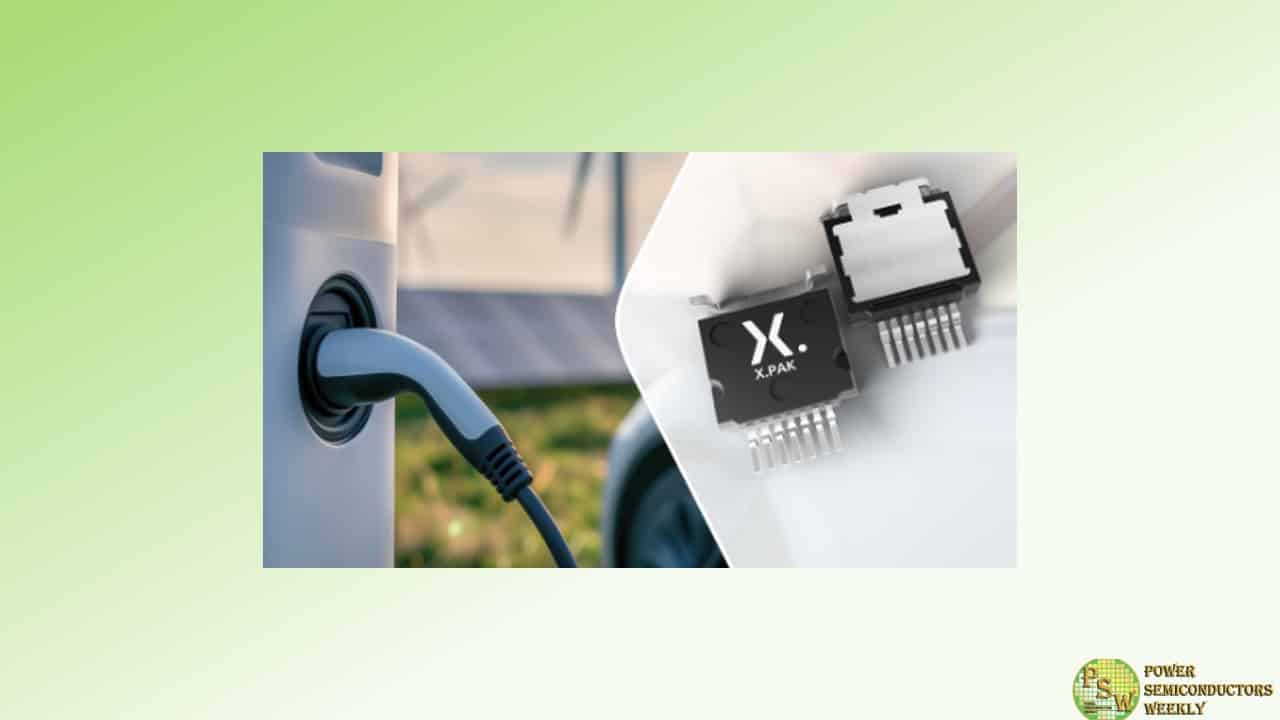
Nexperia introduces a range of highly efficient and robust industrial grade 1200 V silicon carbide (SiC) MOSFETs with industry leading temperature stability in innovative surface-mount (SMD) top-side cooled packaging technology called X.PAK. This package, with its compact form factor of 14 mm x 18.5 mm, combines the assembly benefits of SMD with the cooling efficiency of through-hole technology, ensuring optimal heat dissipation.
This release addresses the growing demand from a broad range of high power (industrial) applications for discrete SiC MOSFETs that harness the advantages of top-side cooling to deliver exceptional thermal performance. These switches are ideal for industrial applications such as battery energy storage systems (BESS), photovoltaic inverters, motor drives, and uninterruptible Power Supplies (UPS). Additionally, they are well-suited for electric vehicle charging infrastructure, including charge piles.
The X.PAK package further enhances the thermal performance of Nexperia’s SiC MOSFETs by reducing the negative impacts of heat dissipation via the PCB. Furthermore, Nexperia’s X.PAK package enables low inductance for surface mount components and supports automated board assembly.
The new X.PAK packaged devices deliver class-leading figures-of-merit (FoM) known from Nexperia SiC MOSFETs, with RDS(on) being a particularly critical parameter due to its impact on conduction power losses. However, many manufacturers concentrate on the nominal value of this parameter and neglect the fact that it can increase by more than 100% as device operating temperatures rise, resulting in significant conduction losses. Nexperia SiC MOSFETs, on the other hand, offer industry-leading temperature stability, with the nominal value of RDS(on) increasing by only 38% over an operating temperature range from 25 °C to 175 °C.
“The introduction of our SiC MOSFETs in X.PAK packaging marks a significant advancement in thermal management and power density for high-power applications,” said Katrin Feurle, Senior Director and Head of SiC Discretes & Modules at Nexperia. “This new top-side cooled product option builds on our successful launches of discrete SiC MOSFETs in TO-247 and SMD D2PAK-7 packages. It underscores Nexperia’s commitment to providing our customers with the most advanced and flexible portfolio to meet their evolving design needs.”
The initial portfolio includes products with RDS(on) values of 30, 40, 60 mΩ (NSF030120T2A0, NSF040120T2A1, NSF060120T2A0), a part with 17 mΩ will be released in April 2025. An automotive qualified SiC MOSFETs portfolio in X.PAK packaging will follow later in 2025, as well as further RDson classes like 80 mΩ.
Original – Nexperia
-

Nexperia announced the launch of 16 new 80 V and 100 V power MOSFETs in the innovative copper-clip CCPAK1212 package, delivering industry-leading power density and outright performance. The innovative copper-clip design provides high current conduction, reduced parasitic inductance, and excellent thermal performance. These features make the devices ideal for motor control, power supplies, renewable energy systems, and other power-hungry applications.
The range also includes application-specific MOSFETs (ASFETs) designed for AI server hot-swap functions. With top-side and bottom-side cooling options, these MOSFETs in CCPAK provide high power density and reliable solutions. All devices are supported by JEDEC registration and Nexperia’s interactive datasheets for seamless integration.
The benchmark PSMN1R0-100ASF is a 0.99 mΩ 100 V power MOSFET capable of conducting 460 A and dissipating 1.55 KW of power, yet in a CCPAK1212 package footprint that occupies only 12mm x 12mm of board space. The PSMN1R0-100CSF offers similar statistics in a top-side cooled version.
The secret to this impressive performance is the internal construction of the devices. The “CC” in CCPAK1212 stands for copper clip, meaning that the power MOSFET silicon die is sandwiched between two pieces of copper, the drain tab on one side and the source clip on the other. With wire bonds entirely eliminated, such an optimized assembly offers a low on-resistance, reduced parasitic inductances, high maximum current ratings and excellent thermal performance.
CCPAK1212 NextPower 80/100 V MOSFETs are recommended for power-hungry industrial applications where high efficiency and high reliability are critical, including brushless DC (BLDC) motor control, switched-mode power supplies (SMPS), battery management systems (BMS) and renewable energy storage. The availability of such power-capable MOSFETs in a single package reduces the need for parallelism, simplifying designs and offering more compact, cost-effective solutions.
The Nexperia CCPAK1212 announcement also includes some new application specific MOSFETs (ASFETs) targeting the hot-swap function in increasingly powerful AI servers. These devices feature an enhanced safe operating area (SOA), providing superior thermal stability during linear mode transitions.
Across all these applications, the availability of top-side and bottom-side cooling options provides engineers a choice of thermal extraction techniques, especially helpful where dissipating heat through the PCB is impractical due to the sensitivity of other components.
“Despite offering market-leading performance, we know that some customers will be reticent to design-in a relatively new package”, stated Chris Boyce, Product Group General Manager at Nexperia. “For this reason, we have registered the CCPAK1212 with the JEDEC standards organization (reference MO-359). We followed a similar approach when we introduced the first LFPAK MOSFET package some years ago and as a result there are now many compatible devices available in the market. You are never on your own for long when your innovations offer genuine value to your customers”, concluded Boyce.
All the new CCPAK1212 MOSFET devices are supported with a range of advanced design-in tools, including thermally compensated simulation models. Traditional PDF datasheets are supplemented with Nexperia’s user-friendly interactive datasheets, which now incorporate a new “graph-to-csv” feature that allows engineers to download, analyze and interpret the data behind each device’s key characteristics. This not only streamlines the design process but enhances confidence in design choices.
Nexperia plans to extend CCPAK1212 packaging to power MOSFETs across all voltage ranges and also to its automotive qualified AEC-Q101 portfolios, addressing the evolving demands of next-generation systems with the highest current and thermal performance requirements.
Original – Nexperia
-

Nexperia introduced a new series of high-performance gate driver ICs designed for driving both high-side and low-side N-channel MOSFETs in a synchronous buck or half-bridge configuration. These devices deliver high current output and excellent dynamic performance, boosting efficiency and robustness in applications.
The automotive-qualified NGD4300-Q100 is ideal for electronic power steering and power converters, while the NGD4300 has been designed for use with DC-DC converters in consumer devices, servers and telecommunications equipment as well as for micro-inverters used in various industrial applications.
The floating high-side driver in these ICs can operate from bus voltages up to 120 V and use a bootstrap supply with an integrated diode, features which simplify overall system design and help to reduce PCB size. They can deliver up to 4 A (peak) source and 5 A of sink current to guarantee short rise and fall times even for heavy loads.
The gate driver has a low 13 ns delay and offers excellent channel-to-channel delay matching of only 1 ns. These delays are significantly lower than for similar competing gate drivers and help to minimize dead-time by maximizing switching duty-cycle. 4 ns rise and 3.5 ns (typical) fall times help to deliver higher efficiency and support high frequency and fast system control. These gate drivers accept input control signals complying with both TTL and CMOS logic levels.
“These devices are the first in our new portfolio of high-performance half-bridge gate drivers” according to Irene Deng, general manager of the IC solutions business group at Nexperia. “This release demonstrates how Nexperia is using process innovation to respond to the burgeoning demand for robust gate drivers that can increase power converter efficiency while also delivering smoother motor control in consumer, industrial and automotive applications.”
For superior robustness in power conversion and motor driving applications, these ICs are fabricated using a silicon-on-insulator (SOI) process. This allows the negative voltage tolerance of the HS pin to extend to -5 V, significantly reducing the risk of damage caused by system parasitic component and unexpected spikes. The NGD4300 and NGD4300-Q100 are available in a choice of DFN-8, SO-8 and HSO-8 packages to offer engineers the flexibility to trade-off between device size and thermal performance, depending on application requirements.
Original – Nexperia
-

Nexperia announced that it has entered into a strategic partnership with KOSTAL, a leading automotive supplier, which will enable it to produce wide bandgap (WBG) devices that more closely match the exacting requirements of automotive applications. Under the terms of this partnership, Nexperia will supply, develop, and manufacture WBG power electronics devices which will be designed-in and validated by Kostal. The collaboration will initially focus on the development of SiC MOSFETs in topside cooled (TSC) QDPAK packaging for onboard chargers (OBC) in electric vehicles (EV).
KOSTAL Automobil Elektrik, with over a century of experience, is a key player in the global automotive industry. Nearly one in every two cars worldwide is equipped with KOSTAL’s products, including more than 4.5 million onboard chargers, contributing to advancements in electromobility. Ranked among the top 100 automotive suppliers globally, KOSTAL is recognized for its innovative, reliable, and cost-optimized solutions. Its long-standing partnerships with customers and employees reflect the company’s commitment to quality and collaboration.
“Nexperia has been a trusted supplier of silicon components to KOSTAL for many years and is delighted to enter into this strategic partnership that will now extend to wide bandgap devices”, according to Katrin Feurle, Senior Director and Head of SiC Discretes & Modules. “KOSTAL will assist in validating our devices in its charging applications, thereby providing us with the type of invaluable ‘real-world’ data that will allow us to further enhance their performance”.
“KOSTAL is extending its’ strategic SiC supply portfolio to support our growth path towards 2030 with a special dedication on E-Mobility applications for onroad and offroad applications” states Dr. Georg Mohr, Executive VP Purchasing & Supply Chain of the KOSTAL Group. “Under this strategic partnership, which reinforces our long- standing customer-supplier relationship, KOSTAL will leverage Nexperia’s expertise in wide bandgap technology, particularly their SiC MOSFETs, which we believe are among the best in the market. By sharing our insights from real-world EV charging applications, we aim to contribute to the development of even more optimized and tailored SiC devices that meet the specific demands of our next-generation solutions.”
Nexperia is among the few companies that is offering a comprehensive range of WBG semiconductor technologies, including SiC diodes and MOSFETs, as well as GaN e-mode and d-mode devices, alongside its established silicon portfolio. With a strong commitment to expanding its commercial WBG offerings, Nexperia is focused on delivering the most suitable products to meet the needs of an increasing range of applications. The company’s focus is to support the responsible use of electrical energy through innovative solutions. Nexperia continues to develop technologies that address the growing demand for efficiency and sustainability in power management.
Original – Nexperia
-
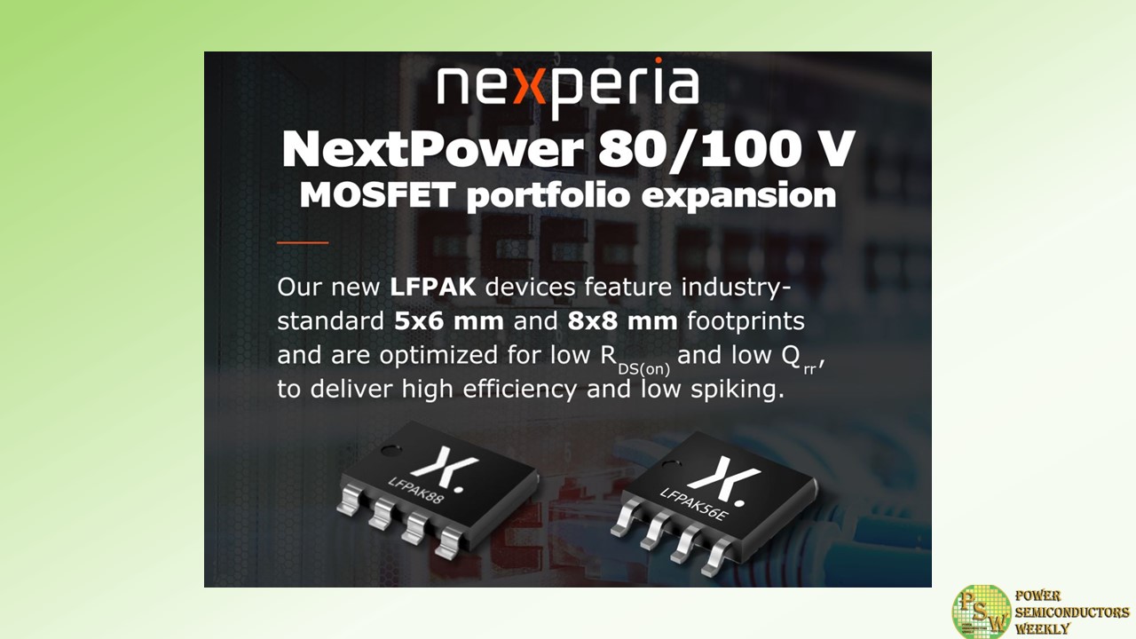
Nexperia announced that the ongoing expansion of its NextPower 80 V and 100 V MOSFET portfolio is continuing apace with the release of several new LFPAK devices in industry-standard 5×6 mm and 8×8 mm footprints. These new NextPower 80/100 V MOSFETs are optimized for low (RDSon) and low Qrr, to deliver high efficiency and low spiking in applications including servers, power supplies, fast chargers and USB-PD as well as for a wide range of telecommunications, motor control and other industrial equipment. Designers can choose from a range of 80 V and 100 V devices, with (RDSon) from 1.8 mΩ to 15 mΩ.
Many MOSFET manufacturers focus on achieving high efficiency through low QG(tot) and low QGD, when benchmarking the switching performance of their devices against alternative offerings. However, through extensive research, Nexperia has identified Qrr as being even just as important due to its impact on spiking and, in turn, the amount of electromagnetic interference (EMI) generated during device switching.
By focusing on this parameter, Nexperia has considerably reduced the level of spiking produced by its NextPower 80/100 V MOSFETs and hence also lowered the amount of EMI they produce. This brings significant benefits for end users by reducing the probability of a costly late-stage redesign to include additional external components if their application fails electromagnetic compatibility (EMC) testing.
The on-resistance (RDSon) of these new MOSFETs has been reduced by up to 31% compared to currently available devices. Nexperia also plans to further strengthen its NextPower 80/100 V portfolio later this year with the release of an additional LFPAK88 MOSFET offering RDS(on) down to 1.2 mΩ @ 80 V, as well as introducing the power dense CCPAK1212 to the portfolio. To further support design-in and qualification of these devices, Nexperia offers the availability of award-winning interactive datasheets, providing engineers with comprehensive and user-friendly insights into device behavior.
Original – Nexperia
-

AIXTRON SE supports Nexperia B.V. in the ramp-up of its 200mm volume production for silicon carbide (SiC) and gallium nitride (GaN) power devices. With the new G10-SiC for the 200mm SiC volume ramp, Nexperia is placing a repeat order for AIXTRON SiC tools. This is complemented by an order for AIXTRON G10-GaN tools.
Both GaN and SiC epitaxial films are essential for the design of next-generation energy-efficient Field-Effect (FET) or Metal-Oxide-Field Effect (MOSFET) transistors to be used in various power conversion applications ranging from data centers and solar inverters in electric vehicles (EV) or trains.
Nexperia has decades of experience in the development of power devices, achieving more than 2.1 billion USD in revenue in 2023. After releasing its first GaN FET device in 2019 and its first SiC MOSFET in 2023, Nexperia continues to expand its portfolio with new high-reliability and power-efficient devices.
Nexperia, headquartered in Nijmegen (Netherlands), operates front-end factories in Hamburg (Germany) and Greater Manchester (England). The AIXTRON epitaxy systems will be installed at Nexperia’s wafer fab in Hamburg (Germany), further strengthening the semiconductor production capabilities in the region. Nexperia’s Hamburg site produces approximately 100 billion discrete semiconductors annually, accounting for about a quarter of the global production of this type of products.
“We are honored to strengthen our alliance with Nexperia, a pivotal player in the semiconductor landscape. Our G10 epitaxy solutions are at the heart of this collaboration, bolstering Nexperia’s growth strategies and enabling the high-volume production of wide bandgap semiconductors for commercial applications. Together, we are setting the pace for the industry’s transition to more energy-efficient SiC and GaN solutions”, said Dr. Felix Grawert, CEO and President of AIXTRON SE.
“As we advance our technological capabilities and market presence in high-power semiconductor production, our strategic partnership with AIXTRON is transformative. Integrating the G10 systems will significantly enhance our wide bandgap technology development and production capabilities. We build on AIXTRON’s proven uniformity and leverage the additional productivity gains of AIXTRON’s G10 tools to scale up our production efficiently and cost-effectively. With the new G10 tools in our Hamburg facility, we are poised for further advancements in our production capabilities,” said Achim Kempe, COO at Nexperia B.V.
Original – AIXTRON
-

Nexperia released 650V ultra- and hyperfast recovery rectifiers in D2PAK Real-2-Pin (R2P) packaging for use in various automotive, industrial and consumer applications including charging adapters, photovoltaic (PV), inverters, servers and switched mode power supplies (SMPS).
Combining planar die technology with a state-of-the-art junction termination (JTE) design, these rectifiers offer high power density, fast switching times with soft recovery and excellent reliability. They are encapsulated in a D2PAK Real-2-Pin Package (SOT8018), which offers the same package outline as the standard D2PAK package but has only two pins instead of three (the middle cathode pin has been removed). This increases the pin-to-pin distance from 1.25mm to over 4mm, which allows to meet the creepage and clearance requirements stated in the IEC 60664 standard.
“These recovery rectifiers further demonstrate Nexperia’s expertise in the field of semiconductor device packaging” according to Frank Matschullat, Head of Product Group Power Bipolar Discretes at Nexperia. “By taking the innovative step of removing the cathode pin from a standard D2PAK package, Nexperia has created a Real-2-Pin package that can meet the creepage and clearance requirements, in particular for high voltage automotive applications.”
Original – Nexperia
-
Semiconductor manufacturer Nexperia announced plans to invest USD 200 million (appx. 184 million Euros) to develop the next generation of wide bandgap semiconductors (WBG) such as silicon carbide (SiC) and gallium nitride (GaN), and to establish production infrastructure at the Hamburg site. At the same time, wafer fab capacity for silicon (Si) diodes and transistors will be increased. The investments are jointly announced with Hamburg’s Minister for Economic Affairs, Dr. Melanie Leonhard, on the occasion of the 100-year anniversary of the production site.
To meet the growing long-term demand for efficient power semiconductors, all three technologies (SiC, GaN, and Si) will be developed and produced in Germany starting in June 2024. This means Nexperia is supporting key technologies in the fields of electrification and digitalization. SiC and GaN semiconductors enable power-hungry applications, such as data centers, to operate with exceptional efficiency and are core building blocks for renewable energy applications and electromobility. These WBG technologies have great potential and are increasingly important for achieving decarbonization goals.
“This investment strengthens our position as a leading supplier of energy-efficient semiconductors and enables us to utilize available electrical energy more responsibly,” comments Achim Kempe, COO and managing director at Nexperia Germany. “In the future, our Hamburg fab will cover the complete range of WBG semiconductors while still being the largest factory for small signal diodes and transistors. We remain committed to our strategy of producing high-quality, cost-efficient semiconductors for standard applications and power-intensive applications, while addressing one of the greatest challenges of our generation: meeting the growing demand for energy and while reducing the environmental footprint.”
First production lines for high-voltage GaN D-Mode transistors and SiC diodes started in June 2024. The next milestone will be modern and cost-efficient 200 mm production lines for SiC MOSFETs and GaN HEMTs. These will be established at the Hamburg factory over the next two years. At the same time, the investment will help to further automate the existing infrastructure at the Hamburg site and expand silicon production capacity by systematically converting to 200 mm wafers. Following the expansion of the clean room areas, new R&D laboratories are being built to continue to ensure a seamless transition from research to production in the future.
In addition to advancing technology, the semiconductor supplier expects the initiative to stimulate local economic development. The investments make an important contribution to securing and creating jobs and enhancing the European Union’s semiconductor self-sufficiency. Nexperia works closely with universities and research institutes to benefit from each other’s expertise and promote highly qualified employee training. Nexperia relies on a robust research and development ecosystem in Hamburg and throughout Europe. Development partnerships and co-operations, e.g. in the field of GaN technology as part of the Industrial Affiliation Program (IIAP) of the nanoelectronics research center imec, play a crucial role. These and other collaborations ensure continuous innovation and technological excellence in Nexperia’s products.
“The planned investment enables us to bring WBG chip design and production to Hamburg. However, SiC and GaN are by no means new territory for Nexperia. GaN FETs have been part of our portfolio since 2019, and in 2023 we expanded our range of products to include SiC diodes and SiC MOSFETs, the latter in collaboration with Mitsubishi Electric. Nexperia is one of the few suppliers to offer a comprehensive range of semiconductor technologies, including Si, SiC, and GaN in both e-mode and d-mode. This means, we offer our customers a one-stop shop for all their semiconductor needs”, explains Stefan Tilger, CFO and managing director at Nexperia Germany.
The investment is yet another milestone in the 100-year history of Nexperia’s production site in Hamburg-Lokstedt. Since the foundation of Valvo Radioröhrenfabrik in 1924, the site has continuously developed and today supplies around a quarter of the global demand for small signal diodes and transistors. Since its spin-off from NXP in 2017, Nexperia has invested substantial sums in the Hamburg site, increased the workforce from 950 to around 1,600 and brought the technological infrastructure up to the state-of-the-art. This continued expenditure underlines the company’s commitment to remaining at the forefront of the industry and providing innovative solutions to its customers worldwide.
Original – Nexperia
-
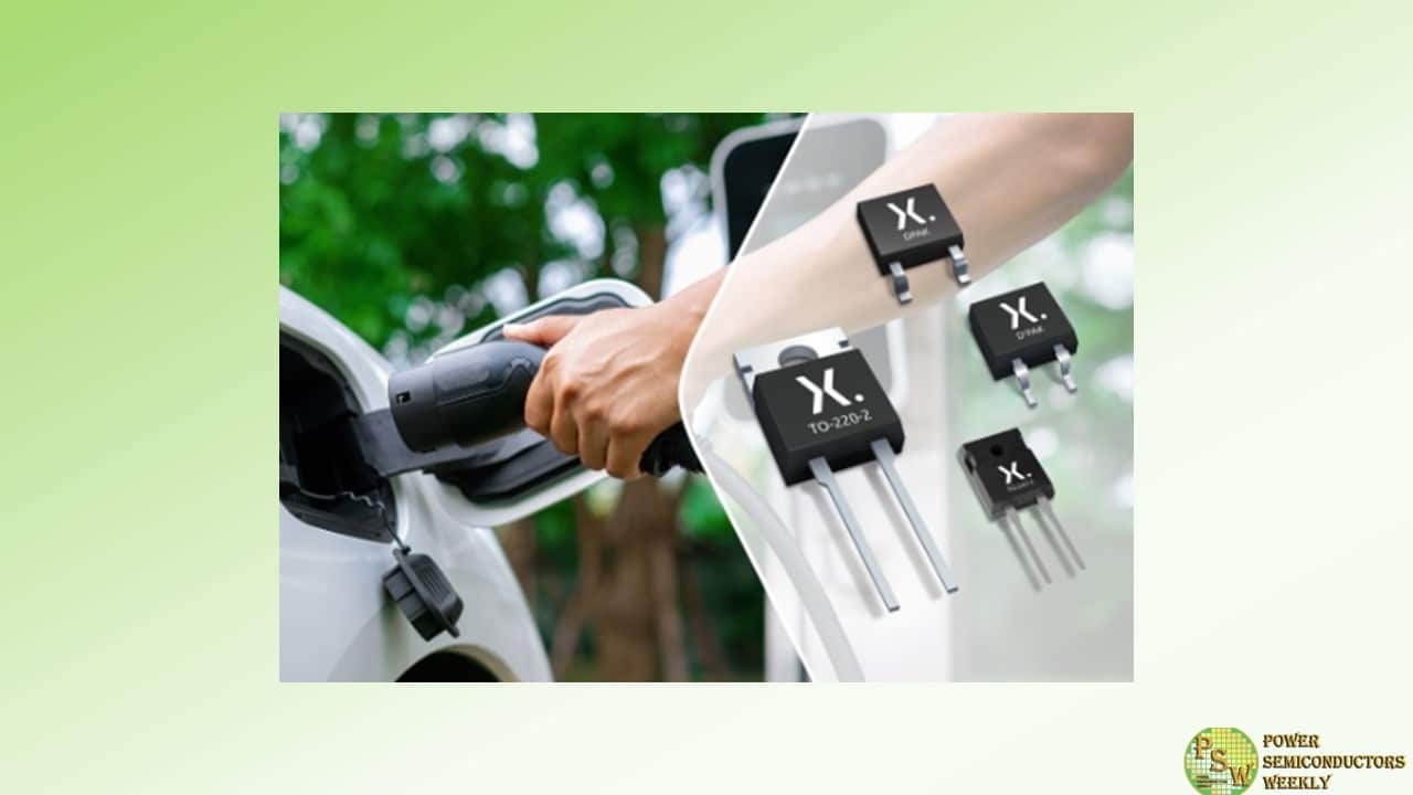
Nexperia announced that its class-leading 650 V, 10 A silicon carbide (SiC) Schottky diode is now automotive qualified (PSC1065H-Q) and available in real-two-pin (R2P) DPAK (TO-252-2) packaging, making it suitable for various applications in electric vehicles and other automobiles.
Additionally, in a further extension to its portfolio of SiC diodes, Nexperia is now also offering industrial-grade devices with current ratings of 6 A, 16 A, and 20 A in TO-220-2, TO-247-2, and D2PAK-2 packaging to facilitate greater design flexibility. These diodes address the challenges of demanding high voltage and high current applications including switched-mode power supplies, AC-DC and DC-DC converters, battery-charging infrastructure, motor drives, uninterruptible power supplies as well as photovoltaic inverters for sustainable energy production.
The merged PiN Schottky (MPS) structure of these devices provides additional advantages over similar competing SiC diodes, including outstanding robustness against surge currents. This eliminates the need for additional protection circuitry, thereby significantly reducing system complexity and enabling hardware designers to achieve higher efficiency with smaller form factors in rugged high-power applications. Nexperia’s consistent quality across various semiconductor technologies provides designers with confidence in the reliability of these diodes.
In addition, Nexperia’s ‘thin SiC’ technology delivers a thinner substrate (one-third of its original thickness) which dramatically reduces the thermal resistance from the junction to the back-side metal. This results in lower operating temperature, higher reliability and device lifetime, higher surge current capability, and lower forward voltage drop.
“We’ve seen an excellent market response to the initial release of our SiC diodes. They have proven themselves in design-ins with one notable example in power supplies for industrial applications, where customers have achieved especially good results. The superior reverse recovery of these diodes translates to high efficiency in real-world use”, says Katrin Feurle, Senior Director and Head of Product Group SiC Diodes & FETs at Nexperia. “We are particularly excited that this is our first automotive-qualified product, and it is already recognized by major automotive players for its performance and reliability.”
Original – Nexperia
