-

Affordability combined with high performance and efficiency is the key to making electric mobility accessible to a broader market. That’s why Infineon Technologies AG is introducing the HybridPACK™ Drive G2 Fusion, establishing a new power module standard for traction inverters in the e-mobility sector.
The HybridPACK Drive G2 Fusion is the first plug’n’play power module that implements a combination of Infineon’s silicon and silicon carbide (SiC) technologies. This cutting-edge solution provides an ideal balance between performance and cost efficiency, giving more choice in the optimization of inverters.
One of the main differences between silicon and SiC in power modules is that SiC has a higher thermal conductivity, breakdown voltage and switching speed, making it more efficient, but also more expensive than silicon-based power modules. With the new module, the SiC content per vehicle can be reduced, while maintaining vehicle performance and efficiency at a lower system cost. For example, system suppliers can realize nearly the system efficiency of a full SiC solution with only 30 percent SiC and 70 percent silicon area.
“Our new HybridPACK Drive G2 Fusion module underlines Infineon’s innovation leadership in the automotive semiconductor industry,” said Negar Soufi-Amlashi, Senior Vice President & General Manager High Voltage at Infineon’s Automotive division. “Addressing the demand for greater e-mobility range, this technological breakthrough smartly combines silicon carbide and silicon. Integrated in a well-introduced module package footprint it offers compelling cost-performance ratio over pure silicon carbide modules without adding system complexity for automotive system suppliers and vehicle manufacturers.”
HybridPACK Drive G2 Fusion expands Infineon’s HybridPACK Drive power module portfolio and can be quickly and easily integrated in vehicle components or modules without requiring complex adjustments or configurations. The HybridPACK Drive G2 Fusion module features up to 220 kW in the 750 V class. It ensures high reliability over the entire temperature range from -40 °C to +175 °C and improved thermal conductivity.
The unique properties of Infineon’s CoolSiC™ technology and its silicon IGBT EDT3 technology with very fast turn-on enable the use of a single gate driver or dual gate drivers. This allows easy re-design from full silicon or full SiC based inverters to a fusion inverter. Generally, Infineon’s holistic expertise in SiC MOSFET and silicon IGBT technology, power module packaging, gate drivers as well as sensors enables premium products with cost savings at system level. One example is the integration of Swoboda or XENSIV™ Hall sensors in the HybridPACK Drive package for more precise and efficient motor control.
Infineon will showcase the new HybridPACK Drive G2 Fusion at electronica 2024 in Munich from November 12 to 15 (hall C3, booth 502).
Original – Infineon Technologies
-

Infineon Technologies AG is intensifying its collaboration with suppliers to further reduce CO 2 emissions along the whole supply chain. Infineon hosted its first ever Supplier Sustainability Summit to further stimulate collaboration and incentivize and support suppliers to accelerate their decarbonization journeys. The virtual event brought together about 100 top semiconductor industry suppliers.
“In order to meet our ambitious targets, we need you, our suppliers,” said Elke Reichart, Member of the Board and Chief Digital and Sustainability Officer at Infineon, during her welcome message. “Infineon’s scope 3 emissions make up the lion’s share of our footprint, especially the materials we source from our suppliers. Therefore, we very much look forward to joining forces with you. Together, we can stimulate and implement decarbonization strategies even better.”
Collaboration with suppliers is a fundamental part of Infineon’s overall sustainability strategy. The company has already made significant progress on its way to reaching climate neutrality by 2030; since 2019 Infineon has halved its CO 2 emissions (scope 1 and 2) while doubling revenue at the same time. In December 2023, Infineon added a commitment to setting a science-based target that includes the supply chain (scope 3). The procurement team is actively working with over 100 suppliers, engaging them to define their own science-based targets and implement appropriate reduction measures.
The Supplier Sustainability Summit was an excellent opportunity for Infineon to share learnings from its own climate strategy and journey and to facilitate exchange of best practices among suppliers. For instance, experts from the Infineon electricity procurement team gave insights from their hands-on experience in achieving 100 percent renewable electricity by 2025; whereas two suppliers shared their expertise in effectively setting science-based targets. The topic was deepened in a panel discussion with Infineon leaders and an expert from the CDP (formerly the Carbon Disclosure Project) that offered further practical advice to attendees.
Infineon’s Green Award recognizes and honors suppliers who demonstrated outstanding environmental commitment and advancements throughout the past year. The “Best Performance Award” went to Applied Materials Inc. for its ambitious climate strategy, including a 1.5°C science-based target and the company’s innovative “Xchange” program. As part of the program Infineon is directly collaborating with Applied Materials to increase resource efficiency and reduce emissions. The program enables take-back and refurbishment of spare parts for complex semiconductor equipment, thereby building on the circular economy to create environmental and business benefits for both parties.
The “Best Improvement Award” winner is Sumco Corporation, that has made remarkable progress in environmental sustainability throughout the past year. The Japan-based company is the first silicon wafer supplier to make a public commitment to setting a science-based target. Following discussions at the top leadership level, Sumco acted at an impressive speed, accelerating existing carbon reduction targets and expanding renewable electricity sourcing.
In the category of companies with less than one billion euros revenue, the “Best Improvement Award” went to iwis SE & Co. KG. The Munich-based, family-owned company serves as a great example to many with its ambitious “Zero Carbon 2040 program” and science-based target commitment. Infineon recognizes the proactive approach towards improving the environmental impact of operations and supply chain and the integration of climate targets in the environmental management system at the sites.
“We would like to applaud the winners of our Green Awards: Applied Materials, Sumco and iwis for stepping up and taking responsibility for environmental sustainability and performance,” said Angelique van der Burg, Chief Procurement Officer at Infineon and host of the day. “We believe that this performance will motivate our whole supplier base to raise the bar higher and follow their example. Now let’s make the best practice a standard practice.”
Original – Infineon Technologies
-

In battery-powered applications such as motor drives and switched-mode power supplies (SMPS), the power supply architecture often requires that a module can be disconnected from the main supply rail when a fault occurs in that module. To achieve this functionality, it is common to use high-side disconnect switches (e.g. MOSFETs) to prevent a load short circuit from affecting the battery.
Infineon Technologies AG introduced the EiceDRIVER™ 1EDL8011, a high-side gate driver designed to protect battery-powered applications such as cordless power tools, robotics, e-bikes, and vacuum cleaners in the event of a fault.
The device provides fast turn-on and turn-off of high-side N-channel MOSFETs with its high gate current capabilities. It consists of an integrated charge pump with an external capacitor to provide strong start-up. The internal charge pump provides the MOSFET gate voltage when the operating input voltage is low. The gate driver IC manages inrush current and provides fault protection. Undervoltage Lockout (UVLO) protection at input voltage prevents the device from operating under hazardous conditions. The driver is available in a DSO-8 package, making it ideal for space-constrained designs. It includes overcurrent protection (OCP), adjustable current setting threshold, time delay and a safe start-up mechanism with flexible blanking during MOSFET turn-on transitions.
The 1EDL8011 has a wide operating voltage range of 8 V to 125 V and a high gate sinking current of up to 1 A, allowing for efficient switching. Additionally, the product has an extremely low off-mode quiescent current of 1 µA, helping to minimize power consumption in sleep mode. The device also includes a V DS sense feature that is used to trigger an overcurrent shutdown by monitoring the drain-to-source voltage of the disconnect MOSFET.
Infineon will be showcasing a demo featuring the 1EDL8011 at its global technology forum OktoberTech™ 2024 in Silicon Valley on 17 October. The 1EDL8011 is available now. Further information can be found at www.infineon.com/1edl8011.
Original – Infineon Technologies
-

Infineon Technologies AG announced a partnership with Canada-based AWL-Electricity Inc., a pioneer in MHz resonant capacitive coupling power transfer technology. Infineon provides AWL-E with CoolGaN™ GS61008P allowing the development of advanced wireless power solutions, enabling new ways to solve power challenges in various industries.
The partnership combines Infineon’s cutting-edge gallium nitride (GaN) technology with AWL-E’s innovative MHz resonant capacitive coupling power transfer system, achieving industry-benchmark wireless power efficiencies. Infineon’s GaN transistor technology offers highest efficiency and highest power density while operating at highest switching frequencies.
This enables AWL-E to increase its system lifetime, reduces downtime and operating costs, and improves ease-of-use for consumers. In the automotive sector, the technology enables a new level of interior experiences and seat dynamics. In industrial systems, it provides near-unconstrained levels of design freedom, such as for automated guided vehicles or robotic applications. Additionally, the technology allows for a fully sealed system design, eliminating the need for charging ports which contributes to reducing global consumption of batteries.
“With our partner approach we prove once more the ability to unlocking the full system-level benefits of Infineon’s CoolGaN technology, enabling compactness and efficiency,” said Falk Herm, Global Partnership & Ecosystem Management at Infineon’s Power & Sensor Systems (PSS) Division at Infineon. “The combination of AWL-E and Infineon’s complementary capabilities demonstrates how the features of GaN, namely operating at MHz frequencies, change the paradigm of what can be done with power transistors, driving greener and better performing products.”
“Infineon uniquely brings you into their family with a recognition that a strong ecosystem ultimately solves today’s power needs,” said Francis Beauchamp-Verdon, Co-founder, VP and Business Development Director at AWL-E. “Infineon’s GaN transistors, eval boards, and partner opportunities have boosted acceptance of our GaN-based MHz power coupling systems.”
Infineon is a leader in the power semiconductor market and currently the only manufacturer mastering all power technologies while offering the broadest product and technology portfolio of silicon (such as SJ MOSFETs, IGBTs), silicon carbide (such as Schottky diodes and MOSFETs) and gallium-nitride-based (e-mode HEMT) devices, covering bare die, discretes, and modules.
Original – Infineon Technologies
-
Data centers are currently responsible for more than two percent of global energy consumption. Fueled by AI, this number is expected to grow to up to around seven percent in 2030, matching the current energy consumption of India. Enabling efficient power conversion from grid-to-core is vital to enable superior power densities and thereby advance compute performance while reducing total cost of ownership (TCO).
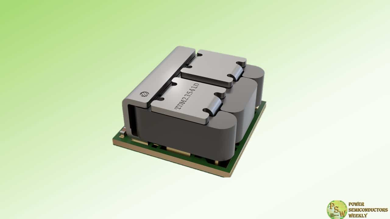
Infineon Technologies AG is therefore launching the TDM2354xD and TDM2354xT dual-phase power modules with best-in-class power density for high-performance AI data centers. These modules enable true vertical power delivery (VPD) and offer industry’s best current density of 1.6 A/mm2. They follow the TDM2254xD dual-phase power modules introduced by Infineon earlier this year.
“We are proud to enable high-performance AI data centers with our TDM2354xT and TDM2354xD VPD modules. These devices will maximize system performance with Infineon’s trademark quality and robustness, thereby enabling best TCO for data centers,” said Rakesh Renganathan, Vice President Power ICs at Infineon Technologies. “Our industry-leading power devices and packaging technologies, combined with our extensive systems expertise, will further advance high-performance and green computing as part of our mission to drive digitalization and decarbonization.”
The TDM2354xD and TDM2354xT modules combine Infineon’s robust OptiMOS™ 6 trench technology, a chip-embedded package that enables superior power density through enhanced electrical and thermal efficiencies, and a new inductor technology to enable lower profile and therefore, true vertical power delivery.
As a result, the modules set new standards in power density and quality to maximize the compute performance and efficiency of AI data centers. The TDM2354xT modules support up to 160 A and are the industry’s first Trans-Inductor Voltage Regulator (TLVR) modules in a small 8 x 8 mm² form factor. Combined with Infineon’s XDP™ controllers, they offer extremely fast transient response and minimize on-board output capacitance by up to 50 percent, further increasing system power density.
The new modules will be showcased at Infineon’s global technology forum OktoberTech™ 2024 in Silicon Valley on 17 October and at electronica 2024 in Munich from November 12 to 14 (hall C3, booth 502).
Original – Infineon Technologies
-
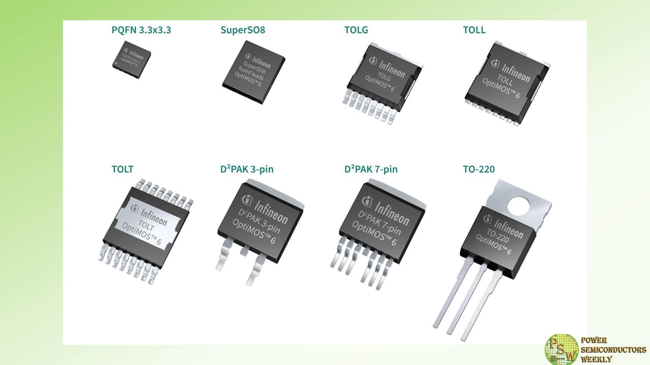
Infineon Technologies AG expands its OptiMOS™ 6 MOSFET portfolio with the new 135 V and 150 V product families. The devices are designed to meet the requirements of drives and switched-mode power supply (SMPS) applications and complement the recently released launched OptiMOS 6 120 V MOSFETs.
With the extended portfolio, Infineon offers its customers a wide range of alternatives to select the best-fit MOSFETs for various applications. Lower switching losses benefit applications like server SMPS, solar optimizers, high-power USB chargers, and telecom. Improved conduction losses are highly beneficial for motor inverters in e-forklifts and light electric vehicles (LEVs).
Compared to the previous generation (OptiMOS 5 150 V MOSFETs), the new product families offer a reduction in on-state resistance R DS(on) of up to 50 percent, while the FOM g is reduced by 20%. With the very low R DS(on), their improved switching performance and excellent EMI behavior, both new families deliver unparalleled efficiency, power density, and reliability. A faster and softer body diode delivers an up to 59 percent lower Q rr, less overshoot and ringing.
The OptiMOS 6 135 V and 150 V MOSFETs are available in a variety of packages to provide customers with a range of options for best-fit products. This broad package portfolio includes TO-220, D 2PAK 3-pin, D 2PAK 7-pin, TOLL, TOLG, TOLT, SuperSO8 5×6 and PQFN 3.3×3.3.
The OptiMOS 6 135 V and 150 V MOSFETs can be ordered now. Further information is available at www.infineon.com/optimos-6-135v and www.infineon.com/optimos-6-150v.
Original – Infineon Technologies
-
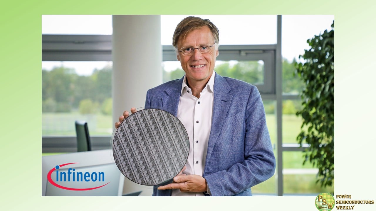
Infineon Technologies AG announced that the company has succeeded in developing the world’s first 300 mm power gallium nitride (GaN) wafer technology. Infineon is the first company in the world to master this groundbreaking technology in an existing and scalable high-volume manufacturing environment. The breakthrough will help substantially drive the market for GaN-based power semiconductors.
Chip production on 300 mm wafers is technologically more advanced and significantly more efficient compared to 200 mm wafers, since the bigger wafer diameter fits 2.3 times as many chips per wafer.
GaN-based power semiconductors find fast adoption in industrial, automotive, and consumer, computing & communication applications, including power supplies for AI systems, solar inverters, chargers and adapters, and motor-control systems. State-of-the art GaN manufacturing processes lead to improved device performance resulting in benefits in end customers’ applications as it enables efficiency performance, smaller size, lighter weight, and lower overall cost. Furthermore, 300 mm manufacturing ensures superior customer supply stability through scalability.
“This remarkable success is the result of our innovative strength and the dedicated work of our global team to demonstrate our position as the innovation leader in GaN and power systems,” said Jochen Hanebeck, CEO of Infineon Technologies AG. “The technological breakthrough will be an industry game-changer and enable us to unlock the full potential of gallium nitride. Nearly one year after the acquisition of GaN Systems, we are demonstrating again that we are determined to be a leader in the fast-growing GaN market. As a leader in power systems, Infineon is mastering all three relevant materials: silicon, silicon carbide and gallium nitride.”
Infineon has succeeded in manufacturing 300 mm GaN wafers on an integrated pilot line in existing 300 mm silicon production in its power fab in Villach (Austria). The company is leveraging well-established competence in the existing production of 300 mm silicon and 200 mm GaN. Infineon will further scale GaN capacity aligned with market needs. 300 mm GaN manufacturing will put Infineon in a position to shape the growing GaN market which is estimated to reach several billion US-Dollars by the end of the decade.
This pioneering technological success underlines Infineon’s position as a global semiconductor leader in power systems and IoT. Infineon is implementing 300 mm GaN to strengthen existing and enabling new solutions and application fields with an increasingly cost-effective value proposition and the ability to address the full range of customer systems. Infineon will present the first 300 mm GaN wafers to the public at the electronica trade show in November 2024 in Munich.
A significant advantage of 300 mm GaN technology is that it can utilize existing 300 mm silicon manufacturing equipment, since gallium nitride and silicon are very similar in manufacturing processes. Infineon’s existing high-volume silicon 300 mm production lines are ideal to pilot reliable GaN technology, allowing accelerated implementation and efficient use of capital. Fully scaled 300 mm GaN production will contribute to GaN cost parity with silicon on R DS(on) level, which means cost parity for comparable Si and GaN products.
300 mm GaN is another milestone in Infineon’s strategic innovation leadership and supports Infineon’s mission of decarbonization and digitalization.
Original – Infineon Technologies
-
Infineon Technologies AG has been nominated for the Deutscher Zukunftspreis 2024, the Federal President’s Award for Technology and Innovation, for its development of a new type of energy-saving chip based on the innovative semiconductor material silicon carbide (SiC). The Jury of Deutscher Zukunftspreis has announced the three nominated teams in Munich.
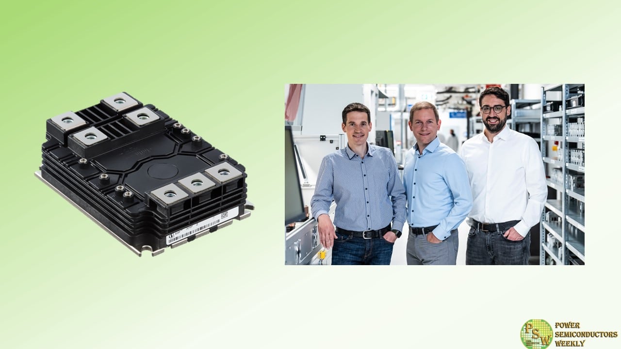
A team of developers from Infineon, together with Chemnitz University of Technology, has succeeded in developing the world’s first silicon carbide MOSFET with a vertical channel (trench MOSFET) and innovative copper contacting in the 3300V voltage class. The new SiC modules and the power converters equipped with the modules represent a revolutionary innovation leap in semiconductor technology from conventional silicon to more energy-efficient silicon carbide, which reduces switching losses in high-current applications by 90%.
MOSFETs are electrical switches for a wide range of applications. Trench MOSFETs differ from so-called planar MOSFETs in their cell structure and performance. While the current flow in planar MOSFETs is initially horizontal, trench MOSFETs offer purely vertical channels. This results in a higher cell density per surface area, which in turn significantly reduces the losses in the chip during energy conversion and therefore increases efficiency.
“The transition towards green energy and many other pressing challenges of our time can only be solved with technological progress,” said Jochen Hanebeck, CEO of Infineon Technologies AG. “It is therefore important to promote and reward innovation and make it visible in society. The ‘Deutscher Zukunftspreis’ is the most important national award that is presented with this aim in mind. The nomination is a great honor for us and proof of the successful research and development work at Infineon. Congratulations to all colleagues involved!”
The CoolSiC™ XHP™2 module family enables significant energy savings, for example in industrial power generation in solar parks or wind turbines, in power transmission and, above all, in end consumption, where high energies in the megawatt range are required. A single train with a silicon carbide drive system can save around 300 MWh per year compared to the previous silicon-based solution. This is roughly equivalent to the annual consumption of 100 single-family homes. Together with drive technology manufacturers and rail operators, Infineon is making an important contribution to decarbonization. At the same time, local residents also benefit from the lower noise level of trains with SiC modules when they pass through residential areas.
Through numerous innovative developments in chip processing and design as well as contacting and module technology, the team led by Dr. Konrad Schraml, Dr. Caspar Leendertz (both Infineon) and Prof. Dr. Thomas Basler (Chemnitz University of Technology) has brought the 3300V CoolSiC XHP2 high-performance module to production readiness. With ten times greater reliability against thermomechanical stress and a significantly higher power density compared to silicon modules, the new silicon carbide module can also be used to electrify large drives in diesel locomotives, agricultural and construction machinery, aircraft and ships, which were previously reserved for fossil fuels. The significantly higher switching frequencies permitted by the new module are helpful, as they enable a significant reduction in weight and volume of the power converters in the application.
“This nomination shows that climate change and sustainable resource consumption have become central aspects of our society,” said Dr. Peter Wawer, Division President Green Industrial Power (GIP) at Infineon. “Innovative energy solutions and power semiconductors are a core component in decarbonization and fighting climate change, as the expert jury of Deutscher Zukunftspreis has recognized. I am proud that we at Infineon can make a significant contribution to a green future with pioneering technology.”
Project manager Dr. Konrad Schraml: “For us as a development team, it is a matter close to our hearts to develop innovative chips that contribute to efficient energy consumption and thus also to green mobility on our planet. This nomination is a great recognition for my team, whose tireless efforts, expertise and passion for sustainability have made the technology breakthrough in silicon carbide possible.”
On November 27, Federal President Frank-Walter Steinmeier presents the Deutscher Zukunftspreis to the winning team in Berlin.
Original – Infineon Technologies
-
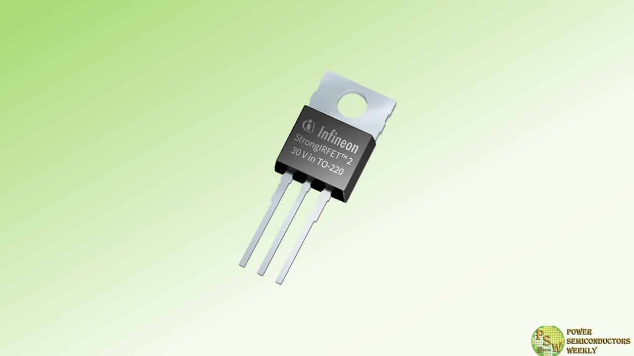
Infineon Technologies AG introduced its new StrongIRFET™ 2 power MOSFET 30 V portfolio, expanding the existing StrongIRFET 2 family to address the growing demand for 30 V solutions in the mass market segment. Optimized for high robustness and ease-of-use, the new power MOSFETs were specifically designed to meet the requirements of a wide range of mass market applications, enabling high design flexibility.
Amongst these applications are industrial switched-mode power supplies (SMPS), motor drives, battery-powered applications, battery management systems, and uninterruptible power supplies (UPS).
The StrongIRFET 2 30 V technology offers up to a 40 percent R DS(on) improvement and up to a 60 percent reduction in Q G compared to the previous generation of StrongIRFET devices. This translates into higher power efficiency for improved overall system performance while providing an excellent robustness.
The new power MOSFETs also ensure an easy design-in and provide simplified product services. The product family’s excellent price/performance ratio makes it an ideal choice for designers looking for convenient selection and purchasing.
The StrongIRFET 2 power MOSFETs in 30 V are available now in a TO-220 package. By the end of 2024, the portfolio will be available in a wider range of industry-standard packages and pin-out options, including to DPAK, D²PAK, PQFN and SuperSO8.
Original – Infineon Technologies
-

STMicroelectronics has joined Quintauris GmbH as its sixth shareholder. ST joins other Quintauris shareholders, Robert Bosch GmbH, Infineon Technologies AG, Nordic Semiconductor ASA, NXP® Semiconductors, and Qualcomm Technologies, Inc.
Quintauris was founded in December 2023 to advance the adoption of products based on RISC-V principles. This will include access to reference architectures, and assistance in the creation of versatile, cross-industry solutions. The initial core industry applications will be for the automotive sector, with a planned expansion to mobile and IoT.
RISC-V is an open-standard Instruction Set Architecture (ISA), originally developed by researchers at the University of California, Berkeley, in 2010.
“ST is a welcome addition to our list of shareholders,” said Alexander Kocher, CEO, Quintauris.“By fostering collaboration between the world’s largest semiconductor companies, we aim to explore and unlock the potential of RISC-V for all the industries we will serve.”
Original – STMicroelectronics
