-
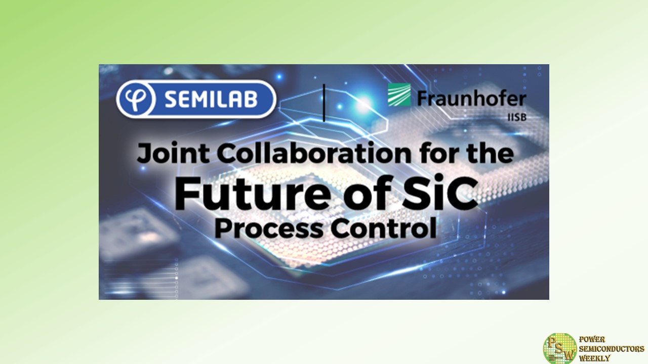
Semilab Zrt. and Fraunhofer IISB announced the official kick-off of their strategic partnership.
Within their new joint lab, located at the IISB in Erlangen, the partners develop state-of-the-art metrology and inspection solutions for (ultra-) wide-bandgap semiconductor materials.
The goal is to take semiconductor metrology to a next level along the value chain, from base material to die. By bringing new features and tools from lab to market, new standards for SiC, GaN and other (U)WBG semiconductors will be set.Original – Fraunhofer IISB
-
Semilab announced an agreement to form a long-term strategic partnership with Fraunhofer IISB. Within the framework of this cooperation, a demo lab will be opened with a strong focus on developing state-of-the-art metrology and inspection solutions for wide bandgap semiconductor materials.
Over the years, developments in compound semiconductor materials such as silicon carbide (SiC) have been receiving increased attention. SiC devices show great promise in the future of wide bandgap semiconductors due to their superior material properties. The silicon carbide market’s growth shows no sign of slowing down due to the expansion in the industrial and automotive sectors. Semilab believes in driving decarbonization by supporting the development of key SiC products and components.
Based in Budapest, Hungary, Semilab is a strategic metrology supplier and innovation partner of the leading wafer manufacturers, IC device makers in the More-than-Moore market segment. Semilab provides state-of-the-art metrology solutions for semiconductor device manufacturers, both in-line and R&D segments. The company is among the world leaders in non-contact CV metrology for SiC and its market share is growing for EPI thickness and resistivity monitoring.
The Fraunhofer IISB in Erlangen, Germany, specializes in wide-bandgap semiconductors and efficient power electronics. Here, device know-how merges with complex system development, especially for e-mobility and sustainable energy supply.
The institute bundles its activities in the two business units Power Electronic Systems and Semiconductors. In doing so, it comprehensively covers the entire value chain from basic materials, through semiconductor device, process and module technologies, to complete electronics and energy systems. As a unique center of excellence in Europe for the semiconductor material silicon carbide (SiC), the IISB is a pioneer in the development of highly efficient power electronics, even for extreme requirements. This spans from material, over process and to device development supported by providing innovative metrology solutions.
Considering the crucial role both players have in shaping of the European semiconductor scene, the strategic partnership between Semilab and Fraunhofer IISB will allow the utilization of their respective resources and global networks in order to develop new, innovative silicon carbide processes and metrologies.
Original – Semilab
