-

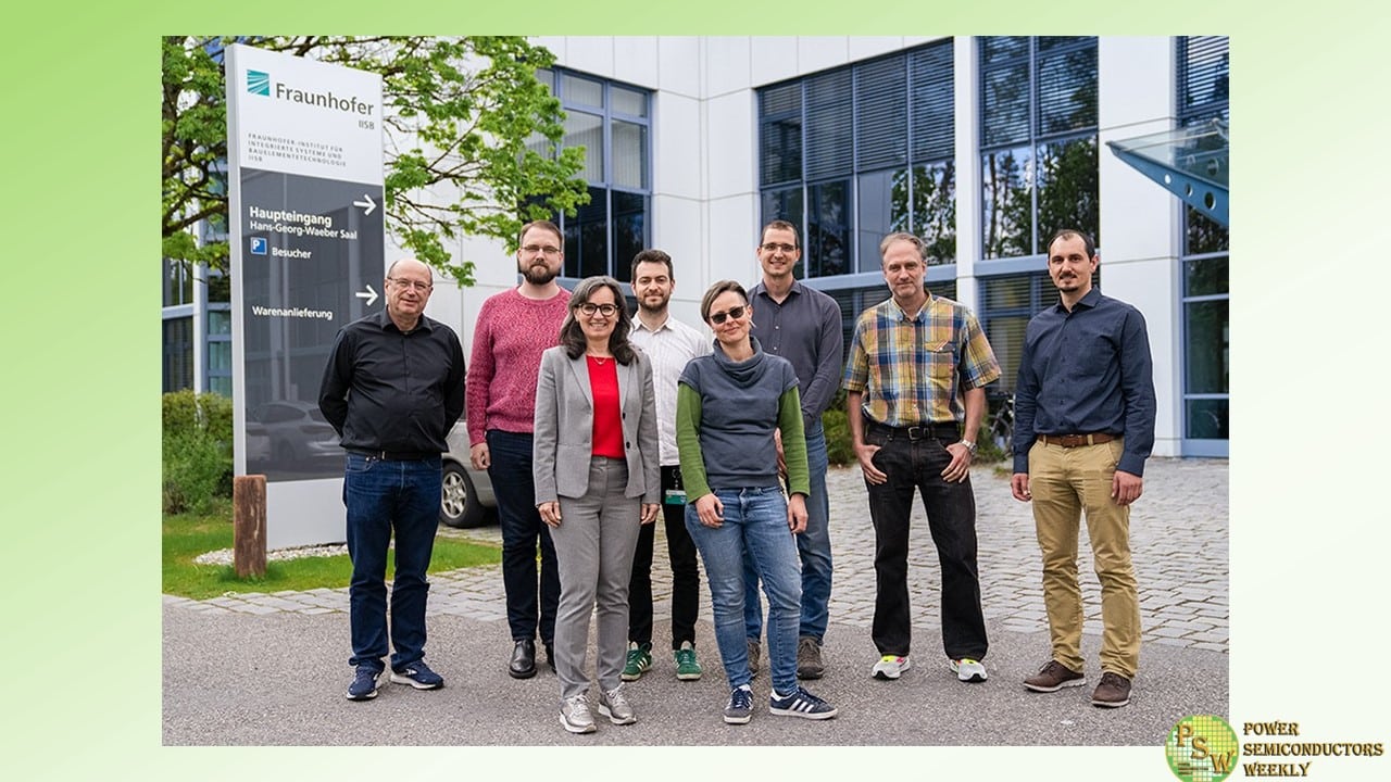
As part of a so-called Joint Lab at Fraunhofer IISB, AIXTRON SE operates equipment, works on process development for SiC epitaxy and runs a demo center for its customers. Joint Labs like this are a great opportunity for companies to collaborate with Fraunhofer IISB in an industry-compatible laboratory environment.
For the epitaxy Joint Lab, the awarded IISB team ensures the continuous fault-free operation of already 5 state-of-the-art G10 SiC reactors, and enables the installation of new systems with minimal downtime. By setting up automated metrology and by optimizing wafer logistics, workflows and data management, the team has also established a modern wafer characterization facility at the IISB with a fast feedback loop for AIXTRON.
Fraunhofer IISB is thrilled for its colleagues Rainer Apelt, Nino Fröbisch and Katharina Roßhirt-Lilla from the SiC Epitaxy Group of the Materials Department together with Christian Heilmann, Rainer Schönweiß and Christopher Torscher from the Infrastructure Group within the Central Services Department. Such outstanding results are the base for the success of the Joint Labs model at Fraunhofer IISB.
Original – Fraunhofer IISB
-
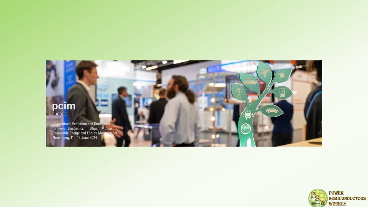
Wide-bandgap (WBG) semiconductor technology and artificial intelligence together are revolutionizing power electronics. A new class of intelligent power electronic systems is unlocking new performance and application areas. The high demands of system development impact the entire power electronics value chain. Specifically, this applies to semiconductor materials and devices as well as packaging and module technology. Extreme operating and environmental conditions demand maximum reliability and ultra-high performance. At PCIM Europe 2024, Fraunhofer IISB, Fraunhofer ISIT and Fraunhofer IMS together present the entire value chain for next-generation power electronics.
All-electric Society
In power electronics, a fundamental change is happening. Two very dynamic sectors are currently automotive electronics and energy technology. In both application areas, there is a race for ever more efficient, high-performance and cost-effective power electronics systems. On top of this, there are increased requirements in terms of the reliability and service life of the electronic parts and components.The main purpose of power electronics is the conversion and distribution of electrical energy using electronic switches between different sources, energy storages and loads that are electrically linked to each other. Power electronics fulfill these functions both in stationary applications, such as integrating renewable energy sources into the power grid, and more and more in mobile applications, like in battery electric vehicles. The central and crucial components here are the electrical converters, which can be used, for example, as chargers, voltage converters or drive inverters.
Faster – Stronger – Higher
With drive outputs of up to 1000 kW and ranges of over 1000 km, electric powertrains for electric cars have reached a new level. The electric converters are operating in the megawatt class. As a result, vehicle electronics are advancing vehemently into the area of larger drives and opening up further interesting fields of application. Outstanding examples are the emerging electrification in ships and aviation.Hybridization, i.e., the combination of combustion engines or jet propulsion systems with fuel cell technology and battery storage, promises enormous savings in terms of fuel consumption and emissions. Alongside batteries, hydrogen is becoming an interesting energy carrier. The hydrogen technology in turn opens up its own technological possibilities, such as the design of cryogenic converters or the use of superconducting cables and motor windings. However, classic silicon components have reached their physical limits and the use of wide-bandgap semiconductors such as silicon carbide or gallium nitride is a necessity.
Taking off with WBG
WBG-based power devices offer low on-state losses, enable higher switching frequencies and can handle high currents at high operating voltages. They provide superior thermal properties and are suitable for operation in a wide temperature range. Customized device and process technologies, such as VDMOS, pave the way to fully exploit the potential of WBG semiconductors for power electronics.In terms of industrial application, SiC (silicon carbide) and GaN (gallium nitride) semiconductor technologies have gained significant impact on the market. However, there are still unlocked advantages at system level in terms of cost, efficiency, and construction volume. Current research activities are focused on an in-depth understanding of device characteristics and materials properties, not only on device level.
In the development of WBG-capable modules, especially GaN and SiC power modules, various technical challenges remain to be investigated. So, to realize highest efficiency power electronic conversion with fast switching, parasitic effects have to be minimized. In this context, the spatial and functional integra-tion of the semiconductor switches with the driver control is crucial.
New challenges for WBG power modules come from extreme temperatures like cryogenic as well as high-temperature applications with appropriate adaptations to the packaging technology. Accordingly extended qualification measures and test procedures are required, that take novel failure mechanism into account. With special environmental and operational conditions, aviation is one of the hardest areas to conquer. Reliability is the key here, as failure rates must be precicely identified and extremely low. And all this with an outstanding power-to-weight ratio.
Power Meets Intelligence
Another trend in system development is apparent: the progressive integration of information and commu-nication technology.On-board power grids for aircrafts and vessels are comparable with the local power grid of a small town in terms of their complexity and dimensions. The grids connect many distributed sources and loads via long cables and transfer high power simultaneously. As a result, the focus is shifting to grid stability and droop control, i.e., the control and synchronization of generators and converters. Additional functions for monitoring, management and communication, as well as intelligent capabilites need to be implemented in the grids: On-board grids are evolving into smart grids. In stationary grid technology, especially in smart grids or local DC grids, as well as in battery systems for battery management, this transformation has been visible for a while now.
The fusion with data processing requires an increasing integration of digital technology components. Microcontrollers and system on chips have long been used in drivers and control circuits for electronic power switches. Approaches from classic signal processing are also being applied, e.g., for forming the alternating current waveform to save space and material-intensive passive filter components. This is also exemplified by modular multi-level converters, which consist of a large number of freely configurable inverter cells and can be used to cover a very wide range of applications and performance.
The Perfect Match
A new class of intelligent power electronics with additional AI functionality, the so-called cognitive power electronics, is currently being developed further. These “perceptive systems” are equipped with sensors to detect various physical parameters and embedded electronics to record and analyze data in real time. Electric drives thereby become integrated intelligent systems that know about their present operating status. Based on methods of machine learning, cognitive power electronic systems can make predictions and react autonomously to internal and external influences and events.The high demands imposed by system developers affect all stages of the power electronics value chain. It is already apparent today that the demanded performance characteristics of the new type of power electronics can no longer be achieved with the existing semiconductor devices and system features. Power semiconductors based on ultra-wide bandgap materials and other innovative devices, such as integrated snubbers or active circuit breakers, are in the pipeline. Accompanying, the transition towards an all-electric society pushes the power electronic systems development to new performance levels.
The integrated power electronic system – the symbiosis of innovative power semiconductor technologies, microelectronics and artificial intelligence – is becoming a reality.
PCIM Europe 2024 Nuremberg – Excelling in Power Electronics
At this year’s leading trade fair for power electronics in Europe – PCIM Europe 2024 in Nuremberg – three Fraunhofer Institutes are teaming up at their joint booth no. 6-368. From June 11 to 13, 2024, the Fraunhofer IISB, Fraunhofer ISIT and Fraunhofer IMS together present the entire value chain for next-generation power electronics.
Visitors can expect exhibits on topics ranging from wide-bandgap and ultra-wide-bandgap semiconductors, (U)WBG-ready packaging and module technology, cryogenic to high-temperature, integrated passives, active fuse components, advanced sensor technology, MEMS integration, ultra-compact power converters and modular multi-level converters to electric powertrains for large-scale drives.
PowerCare – Cognitive Power Electronics with Integrated Failure Protection
The centerpiece of the joint booth and overlap of the expertise of the three partner institutes is the exhibition area for project PowerCare. PowerCare uses a new monitoring concept in the form of a miniaturized motor controller with integrated real-time failure prediction (edge AI) to detect upcoming maintenance needs in advance. This is laying the foundation for a new evolutionary stage of intelligent power modules. Simultaneously, the switch to vertical GaN MOSFETs allows for unrivaled power densities and ruggedness.Within the project, Fraunhofer ISIT works on novel, vertical GaN trench MOSFETs and their behavioral models. Fraunhofer IMS contributes embedded AI models integrated in a PWM controller for failure prediction of electric motors and GaN power semiconductors. Fraunhofer IISB demonstrates GaN MOSFETs and an in-telligent motor control with AI-based condition monitoring of the electric drive. For a market-oriented development of cognitive power electronics, the project partners Siemens AG, X-FAB Dresden GmbH & Co. KG, NXP® Semiconductors Germany GmbH, and TU Dortmund University provide support and valuable practical feedback.
Fraunhofer Institute for Integrated Systems and Device Technology IISB
The Fraunhofer IISB in Erlangen specializes in wide-bandgap semiconductors and efficient power electronics. Here, materials and device know-how merges with complex system development, especially for e-mobility and sustainable energy supply. With its solutions, the institute has been setting benchmarks in energy efficiency and power density, even for extreme operating conditions like in aviation and space.At its long-time no. 1 trade fair, the IISB shows the broad spectrum of its activities in high-performance power electronics. Starting from WBG and UWBG base materials over semiconductor technology with SiC device development and prototype processing, the spectrum ranges to hybrid integration, packaging and module technology. In the area of system integration, visitors await exciting exhibits showcasing medium voltage electronics and advanced SiC and GaN power electronics for automotive, maritime and aircraft applications. Special highlights are a fully integrated aircraft power train in the megawatt class and a crewless electric vertical take-off and landing vehicle for early AI-based forest fire detection.
Fraunhofer Institute for Silicon Technology ISIT
The Fraunhofer ISIT in Itzehoe is one of Europe’s most modern research facilities for microsystems technology and power electronics. At the heart of the institute are its cleanroom facilities, large enough not only to conduct research but also to manufacture the microchips developed on an industrial scale.At PCIM 2024, Fraunhofer ISIT gives insights into current and future activities in the areas power electronics and electronic energy systems. As a part of Fraunhofer’s GaN pilot line, an emerging, independent ecosystem for development activities ranging from epitaxy via device processing to application, the ISIT presents lateral and vertical GaN devices and its processing capabilities as well as GaN-on-QST services.
With the concept Active Reliability, the institute shows condition monitoring techniques and data processing approaches such as data-fusion and digital twin for online state-of-health estimation, lifetime extension, and fault tolerance. Further highlights are the EnergyHub, a DC power router for multi-source integration and high-availability power supply and GaN-based converters for high-efficiency and high-density energy conversion.
Fraunhofer Institute for Microelectronic Circuits and Systems IMS
The Fraunhofer IMS in Duisburg is a trusted research and development partner for industry. Its goal is to develop customized sensor systems for specific needs in the areas of biomedical sensors, optical systems, open-source semiconductors, embedded AI, technology services and even quantum technology.At PCIM Europe 2024, Fraunhofer IMS presents innovative technologies in power electronics and RFID technology. The institute also offers solutions in ASIC and chip design as well as CMOS, MEMS and LiDAR. Its RISC-V processors deliver outstanding performance and improve efficiency and reliability in various applications. With the PredictiveBoX developed at the IMS, AI-based vibration analysis can be carried out and production optimized. In addition, customized vertical GaN switches enable savings of megatons of CO2.
Research Fab Microelectronics Germany
The overall framework is the Research Fab Microelectronics Germany FMD (acronym in German), a cooperation of the Fraunhofer Group for Microelectronics with the Leibniz institutes FBH and IHP. With more than 4,600 employees and a diversity of expertise and infrastructure, the virtual umbrella organization of FMD is the largest association of its kind in Europe. As a pioneer in cross-location and cross-technology cooperation, FMD is actively addressing the current and future challenges of electronics research to ensure the preservation and expansion of Germany’s and Europe’s technological sovereignty.Original – Fraunhofer IISB
-
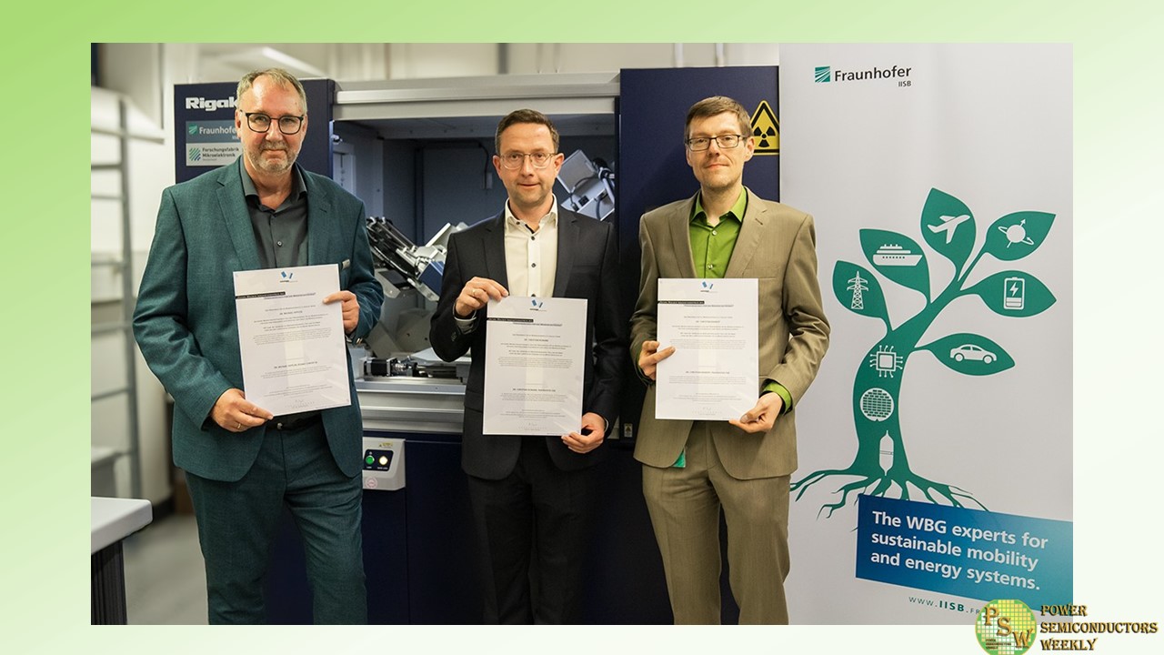
Semilab Zrt. and Fraunhofer IISB announced the official kick-off of their strategic partnership.
Within their new joint lab, located at the IISB in Erlangen, the partners develop state-of-the-art metrology and inspection solutions for (ultra-) wide-bandgap semiconductor materials.
The goal is to take semiconductor metrology to a next level along the value chain, from base material to die. By bringing new features and tools from lab to market, new standards for SiC, GaN and other (U)WBG semiconductors will be set.Original – Fraunhofer IISB
-
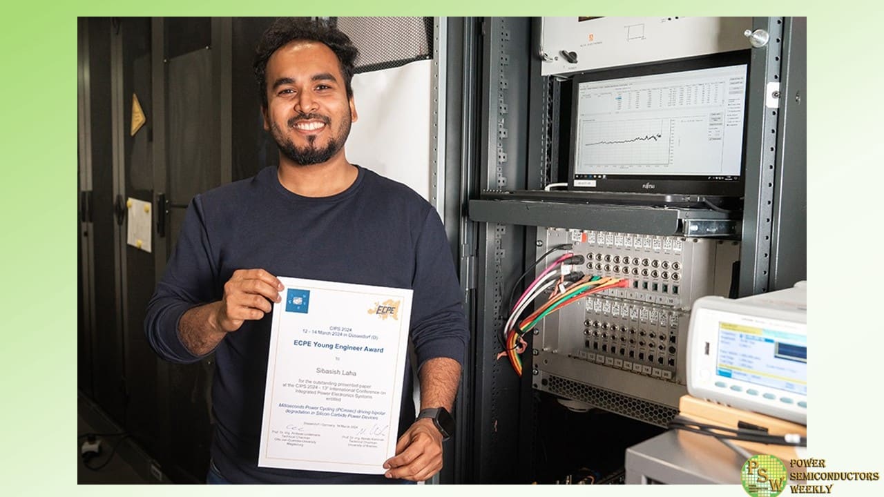
In the paper “Milliseconds Power Cycling (PCmsec) Driving Bipolar Degradation in Silicon Carbide Power Devices”, Sibasish Laha from Fraunhofer IISB and his co-authors Jürgen Leib, Andreas Schletz, Martin Maerz, Christian Liguda, Firas Faisal and Davood Momeni describe an innovative approach to silicon carbide (SiC) power cycling.
Until now, bipolar degradation (BD) tests have not been sufficiently differentiated in the investigation of failure and fault mechanisms for SiC power devices. SiC power products may experience voltage degradation which stems from the stacking faults (SFs) growth, commonly known as BD. To properly evaluate the BD impact on the electric performance of devices, it is important to distinguish it from other stress-related degradation such as power metal or interconnection.
This aspect has not yet been addressed, although the BD mechanism is well understood. The paper outlines a methodology by modifying the power cycling test (PCsec) to PCmsec in order to systematically investigate the effect of BD while controlling the impact of thermal degradation. This method enables a thorough evaluation of the distinct influences of both degradation contributors.
The complete paper will soon be available in the CIPS proceedings. Until then, feel free to download the paper presentation on event page.
There you can also find all our contributions to CIPS 2024:- Modified Approach for the Rainflow Counting Analysis of Temperature Load Signals in Power Electronics Modules – Oral presentation by S. Letz; Co-authors: D. Zhao, J. Leib, B. Eckardt, M. März
- Milliseconds Power Cycling (PCmsec) Driving Bipolar Degradation in Silicon Carbide Power Devices – Oral presentation by S. Laha; Co-authors: D. Momeni, J. Leib, A. Schletz, M. März, C. Liguda, F. Faisal
- Challenges of Junction Temperature Calibration of SiC MOSFETs for Power Cycling – a Dynamic Approach – Poster by J. Breuer, F. Dresel, A. Schletz, J. Klier, J. Leib, M. März, B. Eckardt
- Wide Bandwidth PCB Rogowski Coil Current Sensor with Droop Suppression and DC Restoration for In-Situ Inverter Measurements – Poster by S. Quergfelder, J. Sax, T. Heckel, B. Eckardt, M. März
Original – Fraunhofer IISB
-
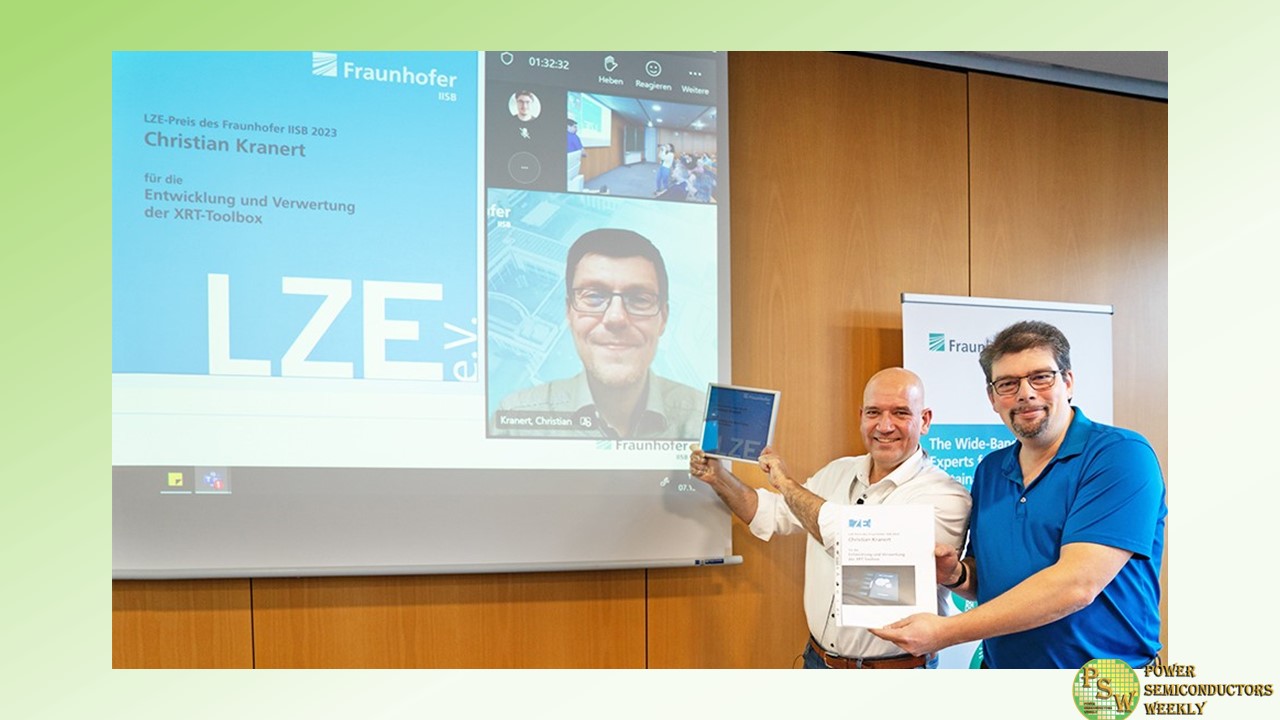
Dr. Christian Kranert, Group Manager Equipment and Defect Simulation of the Materials Department at Fraunhofer IISB, developed a new software for the fast, full-wafer and automated detection and classification of crystal defects in silicon carbide (SiC) substrates. He also pushed the licensing of his new, so-called x-ray ropography (XRT) toolbox to the users of the x-ray topography measuring device XRTmicron from Rigaku. Another highlight is the establishment of two new SEMI International Standards for 4H-SiC defect quantification using XRT test methods.
These outstanding results confirm the success of the Joint Labs model at Fraunhofer IISB. Joint Labs are an exclusive opportunity to collaborate with Fraunhofer IISB in an industry-compatible laboratory environment.
Rigaku Europe SE and Fraunhofer IISB are operating the Center of Expertise for X-ray Topography, a joint lab that is located at the IISB’s headquarters in Erlangen, Germany. This fruitful collaboration is vividly illustrated by the new business in the field of SiC wafer mapping, which Rigaku has built up around its XRTmicron product line in less than two years.
The new LZE Prize honors Fraunhofer IISB employees for exceptional achievements. The LZE Prize is awarded for outstanding acquisitions or particularly successful collaborations, new networks with domestic and foreign partners or above-average achievements in the transfer of know-how from research to industry. The Leistungszentrum Elektroniksysteme (LZE) is a joint initiative of the Fraunhofer-Gesellschaft, Fraunhofer IIS, Fraunhofer IISB, and FAU Erlangen-Nürnberg (FAU), together with industry partners and further research institutes.
Original – Fraunhofer IISB
-
A cross-organizational team from Rigaku SE and Fraunhofer IISB has established a new semicon-ductor material characterization method in their jointly operated Center of Expertise for X-ray Topography in Erlangen, Germany. They succeeded not only in developing an industry-ready X-ray topography system, but also in employing defect detection and quantification algorithms, achieving a worldwide unique material characterization method for silicon carbide (SiC) wafers.
SiC is an excellent semiconductor for application areas like electric mobility and transportation, sustainable energy supply, industrial infrastructure up to sensors and quantum technologies even under harsh operating conditions.
As representatives for the whole research team, Dr. Kranert and Dr. Reimann from Fraunhofer IISB and Dr. Hippler, Managing Director Rigaku Europe SE, have won the Georg Waeber Innovation Award 2023 from the Förderkreis für die Mikroelektronik e.V. (Microelectronics Promotion Society).
Pioneering holistic material defect characterization with X-ray topography
In 2021, Rigaku SE and Fraunhofer IISB have founded the Center of Expertise for X-ray Topography, a joint lab that is located at the IISB’s headquarters in Erlangen, Germany. Here, the cross-organizational team has now developed a new metrology that is non-destructive, robust, reliable, high-throughput and therefore capable of swiftly detecting all relevant crystallographic defects in SiC substrates.
For the first time worldwirde, this innovation realized the holistic approach of setting up the measurement device, i.e., the X-ray topography (XRT) tool as well as formulating appropriate measurement and analysis routines that specifically meet the industry’s demands for speed, reliability, and accuracy. The development process was supported by rigorous scientific validation of the results, a crucial factor for the acceptance of a new approach in the industry.
Until now, no such industry-ready metrology existed for the early stages of SiC power electronics manufacturing, especially at substrate or crystal (commonly referred to as the “puck”) level. This breakthrough in SiC substrate inspection makes it no longer necessary to, e.g., destructively defect etch and discard semiconductor substrates for characterization, as is currently often the case. In consequence, the developed XRT metrology is superior to these existing substrate characterization methods employed in the industry, ultimately leading to substantial cost savings.
Effectively, this technology, developed in Germany, provides everything needed to become the industry standard for specifying and controlling substrate quality in production as well as for R&D substrate and device manufacturers worldwide. The success of this joint innovation is vividly illustrated by the new business, which Rigaku has successfully established in less than two years. Now, the Japan-based company is the world’s leading supplier of XRT tools for SiC substrate and device manufacturing.
The innovative metrology approach has been driven significantly by Dr. Michael Hippler, Managing Director of Rigaku Europe SE, and Dr. Christian Kranert with Dr. Christian Reimann, both group managers in the Fraunhofer IISB’s Materials department. Hence the scientists were selected for the Georg Waeber Innovation Award 2023 by the Förderkreis für die Mikroelektronik e.V. (Microelectronics Promotion Society).
The Förderkreis is an association of industry companies, two Fraunhofer institutes, four chairs of the University of Erlangen-Nuremberg and the Nuremberg Chamber of Commerce and Industry. The main objective is to foster a smooth exchange between science and industry, which is manifested in the Georg Waeber Innovation Award. The award is presented annually for outstanding scientific achievements and places a strong emphasis on the advancement of knowledge in microelectronics and its practical application in the industry. On October 25, 2023, Dr. Hippler, Dr. Reimann and Dr. Kranert received the award during a ceremony at Fraunhofer IISB in Erlangen.
Paving the way for the next generation of SiC power electronics
SiC semiconductor devices play a pivotal role in the power electronics industry. As a replacement for conventional silicon-based power electronics, SiC has the potential to enhance energy efficiency while reducing system costs. It is relevant across various application areas from electric mobility and transportation, sustainable energy supply, industrial infrastructure up to sensors and quantum technologies even under harsh operating conditions.
Consequently, processing low-cost, energy-efficient, and highly reliable SiC power devices is a critical endeavor with the worldwide electrification trend. The production capacities for SiC wafers experience significant growth, which goes hand in hand with an increasing demand for wafer inspection and metrology within the SiC industry. In particular, manufacturers of substrates and power devices require precice information regarding the quality of substrates in terms of crystallographic defects, their distribution across the entire wafer area, and absolute quantities.
Original – Fraunhofer IISB
-
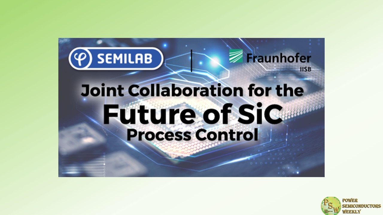
Semilab announced an agreement to form a long-term strategic partnership with Fraunhofer IISB. Within the framework of this cooperation, a demo lab will be opened with a strong focus on developing state-of-the-art metrology and inspection solutions for wide bandgap semiconductor materials.
Over the years, developments in compound semiconductor materials such as silicon carbide (SiC) have been receiving increased attention. SiC devices show great promise in the future of wide bandgap semiconductors due to their superior material properties. The silicon carbide market’s growth shows no sign of slowing down due to the expansion in the industrial and automotive sectors. Semilab believes in driving decarbonization by supporting the development of key SiC products and components.
Based in Budapest, Hungary, Semilab is a strategic metrology supplier and innovation partner of the leading wafer manufacturers, IC device makers in the More-than-Moore market segment. Semilab provides state-of-the-art metrology solutions for semiconductor device manufacturers, both in-line and R&D segments. The company is among the world leaders in non-contact CV metrology for SiC and its market share is growing for EPI thickness and resistivity monitoring.
The Fraunhofer IISB in Erlangen, Germany, specializes in wide-bandgap semiconductors and efficient power electronics. Here, device know-how merges with complex system development, especially for e-mobility and sustainable energy supply.
The institute bundles its activities in the two business units Power Electronic Systems and Semiconductors. In doing so, it comprehensively covers the entire value chain from basic materials, through semiconductor device, process and module technologies, to complete electronics and energy systems. As a unique center of excellence in Europe for the semiconductor material silicon carbide (SiC), the IISB is a pioneer in the development of highly efficient power electronics, even for extreme requirements. This spans from material, over process and to device development supported by providing innovative metrology solutions.
Considering the crucial role both players have in shaping of the European semiconductor scene, the strategic partnership between Semilab and Fraunhofer IISB will allow the utilization of their respective resources and global networks in order to develop new, innovative silicon carbide processes and metrologies.
Original – Semilab
