-
DISCO Corporation opened a new mid-process research center on July 1, 2023.
As the wafers on which circuits are built in the front-end process of semiconductor manufacturing have extremely high added-value, high yield is required in the processes that follow. Among these processes, in the grinding (wafer thinning) and dicing (wafer singulation through cutting) processes handled by DISCO, there is a risk that one processing failure may cause the entire wafer’s quality to deteriorate.
Therefore, caution and accuracy are required for operations such as processing and transfer in particular. In addition, if a large number of defects occur in the back-end process, most of the time, alternative wafers cannot immediately be supplied from the front-end process. As a result, this may have a significant impact on the entire supply chain and become a large issue in the lean manufacturing of the automotive industry.
Recognizing these issues, DISCO has newly positioned these processes that are conventionally in the back-end process of semiconductor manufacturing as part of the “mid-process,” and has been proceeding with R&D in this area.
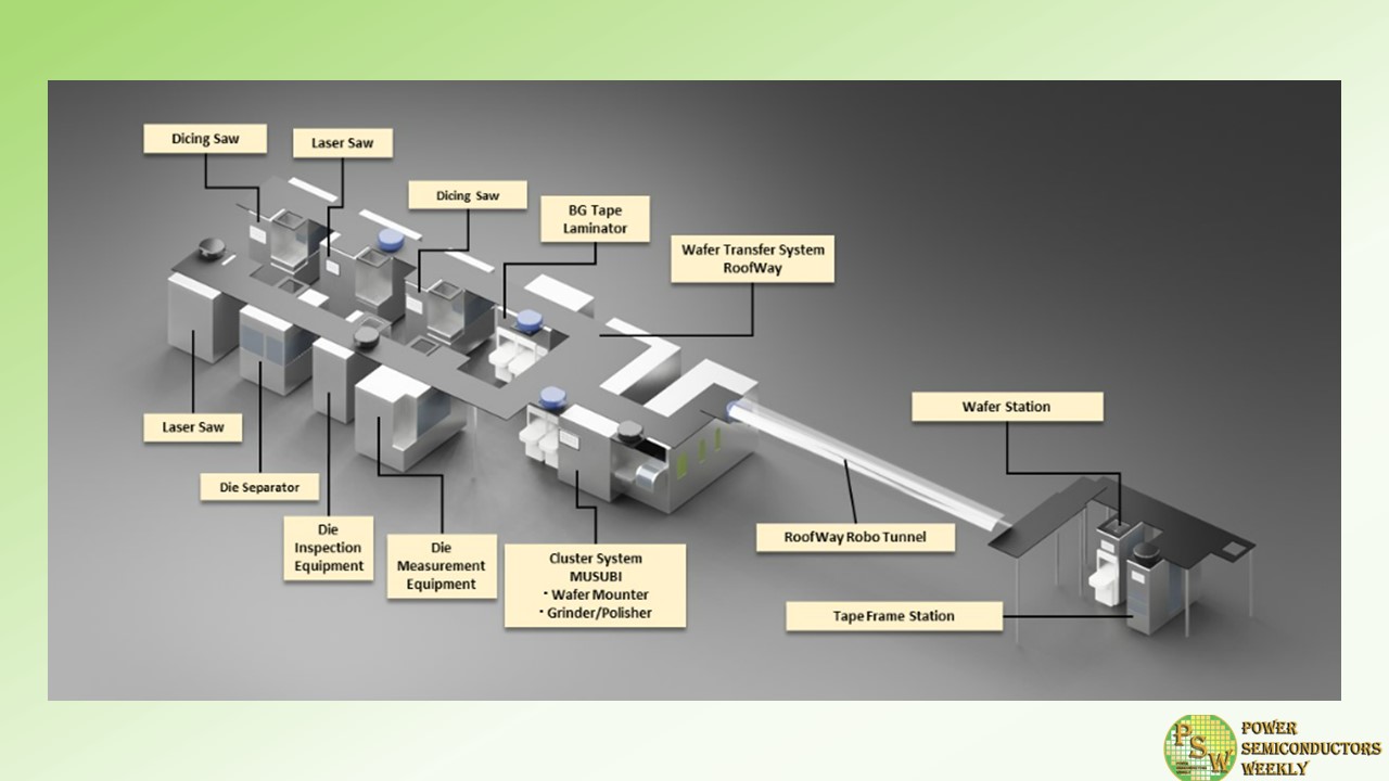
DISCO has officially established the mid-process research center as a site to conduct R&D for the mid-process and perform demonstrations for customers. This center has permanent installations of the wafer transfer system RoofWay as well as the cluster system MUSUBI, and research is underway to reduce the equipment operator’s responsibilities and improve semiconductor wafer processing and transfer quality through automation of the production system.
As semiconductor use in automotive applications is increasing, stricter quality management is being required for semiconductors as well, as they are responsible for the user’s life. Therefore, through this center, DISCO will aim at realizing a production system that eliminates operator intervention as much as possible in order to reduce quality variation that arises from human involvement.
The mid-process research center is a facility that makes verification of unmmaned processes possible by connecting a series of processes with a fully automatic transfer robot. The processes include thinning using a grinder, singulation using dicing saws and laser saws, and pickup, inspection, and measurement of die.
The mid-process research center has been partially open since December 2021, and during the time until the official opening, DISCO has been improving the level of the system by incorporating the valuable opinions of some of the invited customers. Now, as some time has passed from when the category of COVID-19 was downgraded and reclassified as a level 5 infectious disease, DISCO felt that it was finally possible to proactively welcome visitors to the center, and thus decided to make an official announcement for the opening of the center.
Original – DISCO
-
Nexperia launched its entry to the insulated gate bipolar transistor (IGBT) market with a range of 600 V devices, starting with the 30A NGW30T60M3DF. By adding IGBTs to its extensive portfolio, Nexperia is addressing the growing demand for efficient, high-voltage switching devices with a range of performance and cost requirements.
These enable higher power density in power conversion and motor drive applications, including industrial motor drives like servo motors ranging from 5 to 20 kW (20 kHz), robotics, elevators, operating grippers, in-line manufacturing, power inverters, uninterruptible power supply (UPS), photovoltaic (PV) strings, EV-charging, and induction heating and welding.
IGBT is a relatively mature technology. Nonetheless, the market for these devices is expected to grow in line with the increased adoption of solar panels and electric vehicle (EV) chargers. Nexperia’s 600 V IGBTs feature a robust, cost-effective carrier-stored trench-gate advanced field-stop (FS) construction, providing exceptionally low conduction and switching loss performance with high levels of ruggedness in operating temperatures up to 175°C. This improves the efficiency and reliability of power inverters, induction heaters, welding equipment and industrial applications like motor drives and servos, robotics, elevators, operating grippers, and in-line manufacturing.
Designers can choose between the medium speed (M3) and high speed (H3) series IGBTs. These IGBTs have been designed with very tight parameter distributions, allowing multiple devices to connect safely in parallel. In addition, lower thermal resistance than competing devices enables them to provide higher output power. These IGBTs are also fully rated as soft fast reverse-recovery diodes. This means they are suitable for rectifier and bi-directional circuit applications or to protect against overcurrent conditions.
“With the release of these IGBTs, Nexperia provides designers with a greater choice of power-switching devices for a broad range of power applications”, according to Dr. Ke Jiang, General Manager Business Group Insulated-Gate Bipolar Transistors & Modules at Nexperia. “IGBTs are the ideal complement to Nexperia’s existing range of CMOS and wide-bandgap switching devices, making Nexperia a one-stop-shop for power electronics designers.”
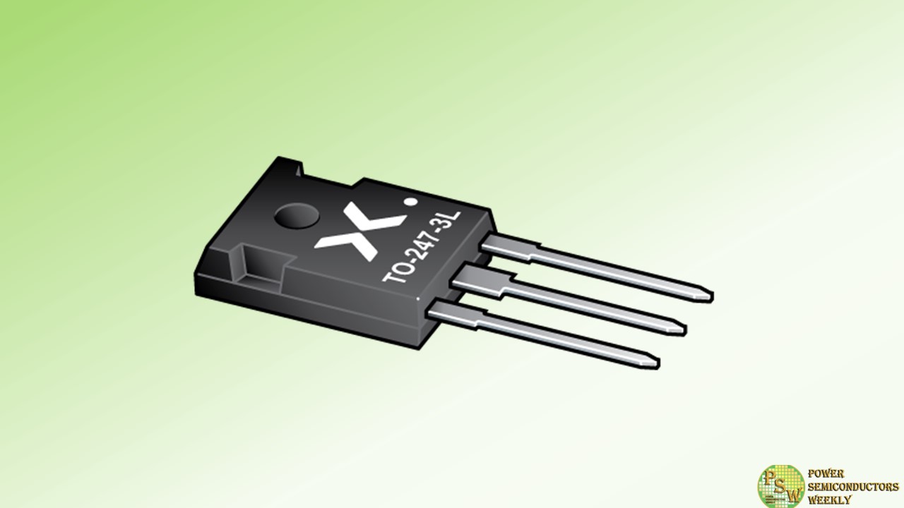
These IGBTs are available in a standard, lead-free, TO247-3L package and are HV-H3TRB qualified for outdoor applications. Nexperia plans to follow this release with a series of 1200 V IGBTs. To learn more about Nexperia’s IGBTs, visit: https://www.nexperia.com/igbts
Original – Nexperia
-

Navitas Semiconductor has confirmed continued supply of leading-edge gallium nitride (GaN) power ICs. On July 3rd, 2023, China’s Ministry of Commerce announced it would put in place certain restrictions on the exporting of gallium and germanium, among other materials, starting in August. Navitas’ wafer technology is ‘GaN-on-Si’. The wafer subcontract manufacturer has verified that their production remains unaffected by the export restrictions, given multiple sources of gallium world-wide.
As a result, Navitas does not expect customer deliveries to be impacted or its business to be adversely affected by the export restrictions.
Significant sources of gallium are available worldwide, as it is a natural by-product in the production of other metals such as aluminum. Navitas does not use germanium in any product.
Original – Navitas Semiconductor
-
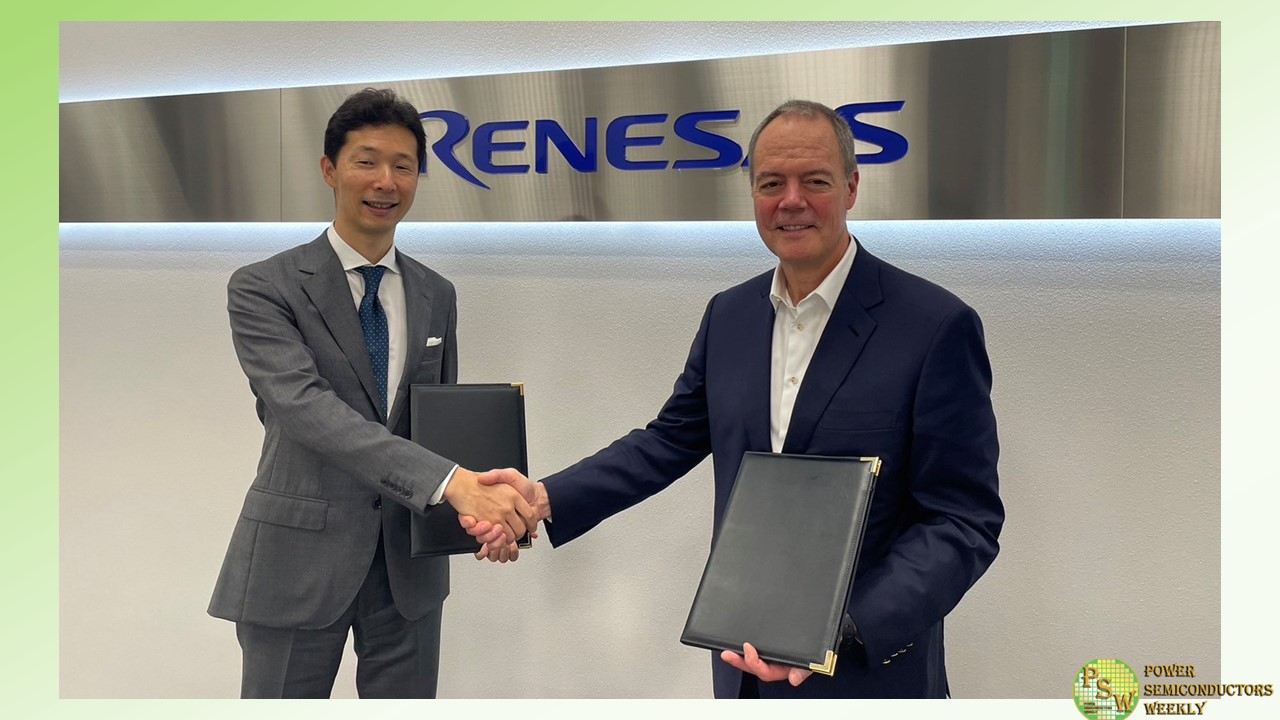
Renesas Electronics Corporation and Wolfspeed, Inc. announced the execution of a wafer supply agreement and $2 billion (USD) deposit by Renesas to secure a 10 year supply commitment of silicon carbide bare and epitaxial wafers from Wolfspeed. The supply of high-quality silicon carbide wafers from Wolfspeed will pave the way for Renesas to scale production of silicon carbide power semiconductors starting in 2025. The signing ceremony of the agreement was held at Renesas’ headquarters in Tokyo between Hidetoshi Shibata, President and CEO of Renesas, and Gregg Lowe, President and CEO of Wolfspeed.
The decade-long supply agreement calls for Wolfspeed to provide Renesas with 150mm silicon carbide bare and epitaxial wafers scaling in CY2025, reinforcing the companies’ vision for an industry-wide transition from silicon to silicon carbide semiconductor power devices. The agreement also anticipates supplying Renesas with 200mm silicon carbide bare and epitaxial wafers after the recently announced John Palmour Manufacturing Center for Silicon Carbide (the “JP”) is fully operational.
The need for more efficient power semiconductors, which supply and manage electricity, is dramatically increasing throughout automotive and industrial applications, spurred by the growth of electric vehicles (EVs) and renewable energy. Renesas is moving quickly to address the growing demand for power semiconductors by expanding its in-house manufacturing capacity. The company recently announced the restart of its Kofu Factory to produce IGBTs, and establishment of a silicon carbide production line at its Takasaki Factory.
Compared to conventional silicon power semiconductors, silicon carbide devices enable higher energy efficiency, greater power density and a lower system cost. In an increasingly energy-conscious world, the adoption of silicon carbide is becoming ever more pervasive across multiple high-volume applications spanning EVs, renewable energy and storage, charging infrastructure, industrial power supplies, traction and variable speed drives.
“The wafer supply agreement with Wolfspeed will provide Renesas with a stable, long-term supply base of high-quality silicon carbide wafers. This empowers Renesas to scale our power semiconductor offerings to better serve customers’ vast array of applications,” said Hidetoshi Shibata, President and CEO of Renesas. “We are now poised to elevate ourselves as a key player in the accelerating silicon carbide market.”
“With the steepening demand for silicon carbide across the automotive, industrial and energy sectors, it’s critically important we have best-in-class power semiconductor customers like Renesas to help lead the global transition from silicon to silicon carbide,” said Gregg Lowe, President and CEO of Wolfspeed. “For more than 35 years, Wolfspeed has focused on producing silicon carbide wafers and high-quality power devices, and this relationship marks an important step in our mission to save the world energy.”
The Renesas $2 billion deposit will help support Wolfspeed’s ongoing capacity construction projects including the JP, the world’s largest silicon carbide materials factory in Chatham County, North Carolina. The state-of-the-art, multi-billion-dollar facility is targeted to generate a more than 10-fold increase from Wolfspeed’s current silicon carbide production capacity on its Durham, North Carolina campus. The facility will produce primarily 200mm silicon carbide wafers, which are 1.7x larger than 150mm wafers, translating into more chips per wafer and ultimately, lower device costs.
Original – Renesas Electronics
