-

STMicroelectronics reported second quarter net revenues of $3.23 billion, gross margin of 40.1%, operating margin of 11.6%, and net income of $353 million or $0.38 diluted earnings per share.
Jean-Marc Chery, ST President & CEO, commented:
- “Q2 net revenues were above the midpoint of our business outlook range driven by higher revenues in Personal Electronics, partially offset by lower than expected revenues in Automotive. Gross margin was in line with expectations.”
- “First half net revenues decreased 21.9% year-over-year, mainly driven by a decrease in Microcontrollers and Power and Discrete segments. Operating margin was 13.8% and net income was $865 million.”
- “During the quarter, contrary to our prior expectations, customer orders for Industrial did not improve and Automotive demand declined.”
- “Our third quarter business outlook, at the mid-point, is for net revenues of $3.25 billion, decreasing year-overyear by 26.7% and increasing sequentially by 0.6%; gross margin is expected to be about 38%, impacted by about 350 basis points of unused capacity charges.”
- “We will now drive the Company based on a plan for FY24 revenues in the range of $13.2 billion to $13.7 billion. Within this plan, we expect a gross margin of about 40%.”
Original – STMicroelectronics
-

The third edition of the second-level master’s program in “Power Electronics Devices and Technologies” organized by the Department of Electrical, Electronic and Information Engineering (DIEEI) of the University of Catania together with STMicroelectronics has been announced.
The goal of the master’s program is to train specialists in technologies based on Wide Band-Gap semiconductors, the new frontier of power electronics that ensures more efficient performance in line with the sustainable development goals defined by Agenda 2030. These technologies are for use in production processes in industries such as automotive, renewable energy, and electrical energy conversion and storage.
“There is a strong market demand for highly specialized professionals trained in the field of power electronics, to meet the needs identified by macro-trends in terms of energy efficiency and the electrification of mobility in the frame of sustainable development,”said Professor Mario Cacciato, coordinator of the master’s program.
“This second-level master’s program offers to master’s graduates in different STEM disciplines opportunities to complete the training and focus it on topics of great interest for research and industry. In addition, the master’s program constitutes a synergistic model for the professional development of young talent from academia together with the industrial world, as effectively demonstrated by the first two editions of the master’s program.”
“STMicroelectronics’ site in Catania is a center of excellence in the European arena for power electronics technologies, thanks in part to the strategic investment in the vertically integrated production of Silicon Carbide devices,” said Gianfranco Di Marco, Power Transistor Sub-Group, Chief of staff and Technical Communication Manager at STMicroelectronics.
“Training specialized profiles and skills in the field of power electronics with multidisciplinary knowledge is essential for fostering technological innovation. This third edition follows the success of the previous ones with theoretical lectures held at University of Catania and internships at ST’s Catania site allowing students to experience working with a leader in power semiconductors. This will forge a close connection between the world of education and the world of work, an essential prerequisite for the sustainable development of the area, and the creation of new career opportunities for students.”
The second-level master’s program offers theoretical and practical training, divided into 7 teaching modules in English. Lectures will be taught by university professors and appropriate specialists from within STMicroelectronics, who will also act as mentors during their internship in the company’s departments and research laboratories. Some lectures, moreover, will be held at ST’s Catania site. Finally, students will participate in seminars held by experts from several major world’s corporations in the industry.
The training course is open to those with a master’s degree obtained in the last five years in:
- Electronic engineering (LM/29);
- Electrical engineering (LM/28);
- Computer and information engineering (LM/32);
- Mechanical engineering (LM/33);
- Chemical engineering (LM22);
- Automation engineering (LM25);
- Telecommunications engineering (LM/27);
- Physics (LM17);
- Materials science and engineering (LM/53);
- Chemical sciences (LM/54);
Proficiency in English is required.
A maximum of 30 participants will be admitted to this master’s degree program. The top 10 in the eligible list will be awarded a scholarship. Those ranking from 11th to 20th will receive a contribution to the tuition fee. Applications must be submitted by September 30, 2024. More information is available here.
The Scientific Committee members are the University of Catania faculty members Mario Cacciato (coordinator), Giuseppe Compagnini, Guglielmo Guido Condorelli, Salvatore Mirabella, Salvatore Pennisi and Antonio Terrasi; and Giuseppe Arena, Michele Calabretta, Gianfranco Di Marco, Vincenzo Randazzo, Mario Saggio, Rosario Scollo, Filippo Scrimizzi and Gabriele Bellocchi of STMicroelectronics.
Original – STMicroelectronics
-
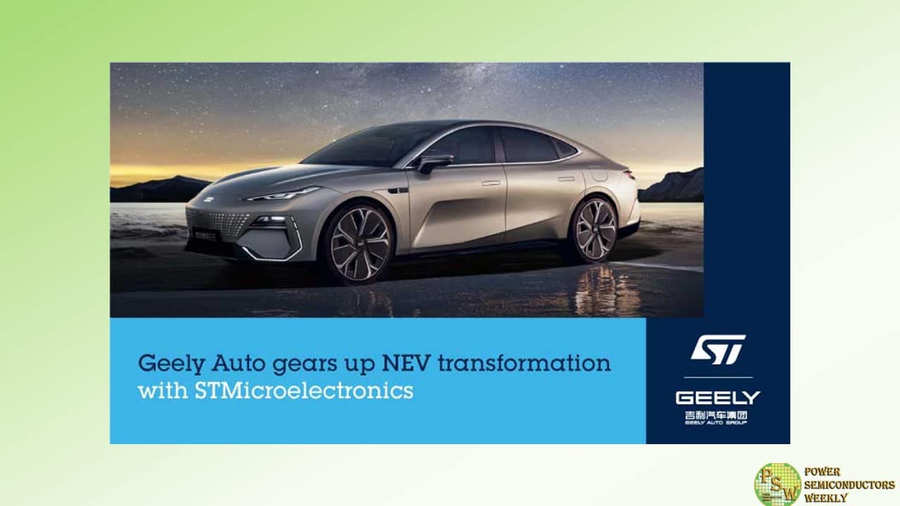
STMicroelectronics and Geely Auto Group have signed a long-term Silicon Carbide (SiC) supply agreement to accelerate their existing cooperation on SiC devices. Under the terms of this multi-year contract, ST will provide multiple Geely Auto brands with SiC power devices for mid-to-high-end battery electric vehicles (BEVs), boosting Geely Auto’s NEV transformation strategy with improved performance, faster charging speeds and extended driving range.
In addition, building on their longstanding cooperation across multiple automotive applications, Geely and ST have established a joint lab to exchange information and explore innovative solutions related to automotive Electronics/Electrical (E/E) architectures (i.e. in-vehicle infotainment, smart cockpit systems), advanced driver assistance (ADAS), and NEVs.
Geely Auto Group has adopted ST’s third generation SiC MOSFET devices in electric traction inverters. The traction inverter is the core of electric powertrains and SiC MOSFETs maximize their efficiency. The combination of advanced inverter design with high-efficiency power semiconductors, like SiC, is the key to superior electric vehicle performance.
“We are very pleased to establish a win-win cooperation with STMicroelectronics, to empower each other and fully utilize our respective advantages and resources.I believe that through the form of innovation joint lab, Geely and ST can deepen our cooperation, achieve mutual benefit, and accelerate the development and implementation of innovative technologies in Geely Auto,” said Li Chuanhai, President of Electronic and Electrical Center of Geely Automotive Central Research Institute.
“We are pleased to have a deep cooperation with global automotive semiconductor leader STMicroelectronics to establish an innovation joint lab. Both sides will deepen long-term cooperation in fields such as smart driving to jointly focus on customer needs, accelerate the implementation of new products and solutions, and shape an efficient cooperation mode. I believe that this cooperation will be beneficial for both parties to conduct more forward-looking technical research based on the development trends of smart, electrified, and connected cars. Geely is delighted to leverage STMicroelectronics’ leading automotive business solutions to be well positioned in product performance, system integration, and overall market competitiveness,” said Fu Zhaohui, Director of the Electronic and Electrical Center of Geely Automotive Central Research Institute.
“Geely Auto, is a shining example of automotive innovation in China, making rapid progress in car electrification and digitalization, while expanding its presence in the global market. This long-term SiC supply agreement and the joint lab establishment mark a significant step forward in our long-established cooperation,” said Henry Cao, Executive Vice President of Sales & Marketing, China Region, STMicroelectronics. “China is the biggest NEV market worldwide and a leading innovator. Our local competence centers and joint labs with our customers across the value chain of automotive allow ST to better support automotive innovation and transformation in China.”
As a leading global automobile manufacturer and China’s top automotive brand, Geely Auto sold a total of 1.68 million vehicles in 2023, with NEV sales reaching 480,000 units, accounting for 28% of the Company’s total sales for the year. This NEV sales volume represents a year-over-year increase of 48%, demonstrating Geely Auto’s successful transition towards NEV and its growing impact in the industry.
With a state-of-the-art SiC manufacturing process and a completely vertically integrated supply-chain, ST provides SiC devices for a wide range of EV applications including traction inverter, OBC (onboard charger), DC-DC converter, EV charging station and e-compressor application, significantly enhancing the performance, efficiency, and range of NEVs. In June 2023, ST and Sanan Optoelectronics, a market leader in compound semiconductors in China, announced the creation of a new 200mm SiC device manufacturing JV in Chongqing, China. This facility will better support the needs of Chinese customers as ST collaborates with more leading Chinese carmakers, industrial customers, and solution providers in SiC, to accelerate the pace of electrification in China.
Original – STMicroelectronics
-
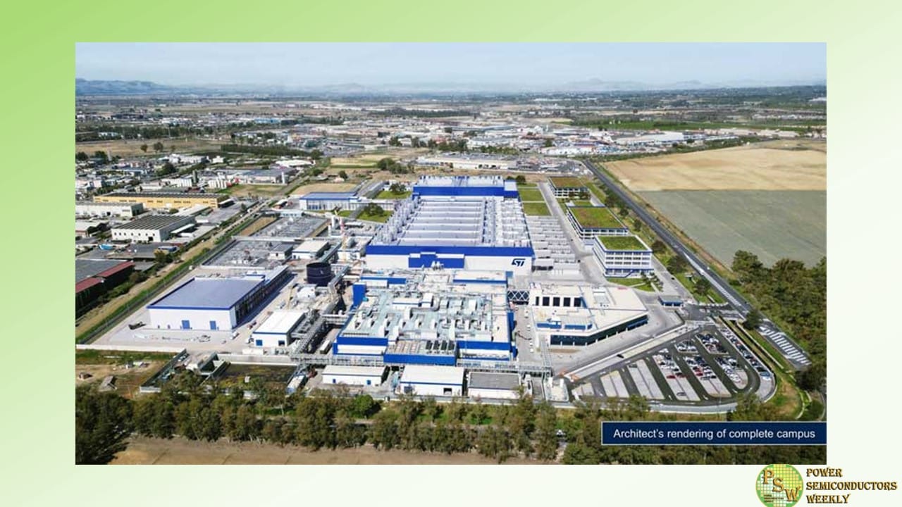
STMicroelectronics announced a new high-volume 200mm silicon carbide (“SiC”) manufacturing facility for power devices and modules, as well as test and packaging, to be built in Catania, Italy. Combined with the SiC substrate manufacturing facility being readied on the same site, these facilities will form ST’s Silicon Carbide Campus, realizing the Company’s vision of a fully vertically integrated manufacturing facility for the mass production of SiC on one site.
The creation of the new Silicon Carbide Campus is a key milestone to support customers for SiC devices across automotive, industrial and cloud infrastructure applications, as they transition to electrification and seek higher efficiency.
“The fully integrated capabilities unlocked by the Silicon Carbide Campus in Catania will contribute significantly to ST’s SiC technology leadership for automotive and industrial customers through the next decades,” said Jean-Marc Chery, President and Chief Executive Officer of STMicroelectronics. “The scale and synergies offered by this project will enable us to better innovate with high-volume manufacturing capacity, to the benefit of our European and global customers as they transition to electrification and seek more energy efficient solutions to meet their decarbonization goals.”
The Silicon Carbide Campus will serve as the center of ST’s global SiC ecosystem, integrating all steps in the production flow, including SiC substrate development, epitaxial growth processes, 200mm front-end wafer fabrication and module back-end assembly, as well as process R&D, product design, advanced R&D labs for dies, power systems and modules, and full packaging capabilities. This will achieve a first of a kind in Europe for the mass production of 200mm SiC wafers with each step of the process – substrate, epitaxy & front-end, and back-end – using 200 mm technologies for enhanced yields and performances.
The new facility is targeted to start production in 2026 and to ramp to full capacity by 2033, with up to 15,000 wafers per week at full build-out. The total investment is expected to be around five billion euros, with a support of around two billion euros provided by the State of Italy within the framework of the EU Chips Act. Sustainable practices are integral to the design, development, and operation of the Silicon Carbide Campus to ensure the responsible consumption of resources including water and power.
Original – STMicroelectronics
-
STMicroelectronics N.V. reported U.S. GAAP financial results for the first quarter ended March 30, 2024. ST reported first quarter net revenues of $3.47 billion, gross margin of 41.7%, operating margin of 15.9%, and net income of $513 million or $0.54 diluted earnings per share. Jean-Marc Chery, ST President & CEO, commented:
- “Q1 net revenues and gross margin both came in below the midpoint of our business outlook range, driven by lower revenues in Automotive and Industrial, partially offset by higher revenues in Personal Electronics.”
- “On a year-over-year basis, Q1 net revenues decreased 18.4%, operating margin decreased to 15.9% from 28.3% and net income decreased 50.9% to $513 million.”
- “During the quarter, Automotive semiconductor demand slowed down compared to our expectations, entering a deceleration phase, while the ongoing Industrial correction accelerated.”
- “Our second quarter business outlook, at the mid-point, is for net revenues of $3.2 billion, decreasing yearover-year by 26.0% and decreasing sequentially by 7.6%; gross margin is expected to be about 40%.”
- “We will now drive the Company based on a revised plan for FY24 revenues in the range of $14 billion to $15 billion. Within this plan, we expect a gross margin in the low 40’s.”
- “We plan to maintain our Net Capex plan for FY24 at about $2.5 billion focusing on our strategic manufacturing initiatives.”
Original – STMicroelectronics
-
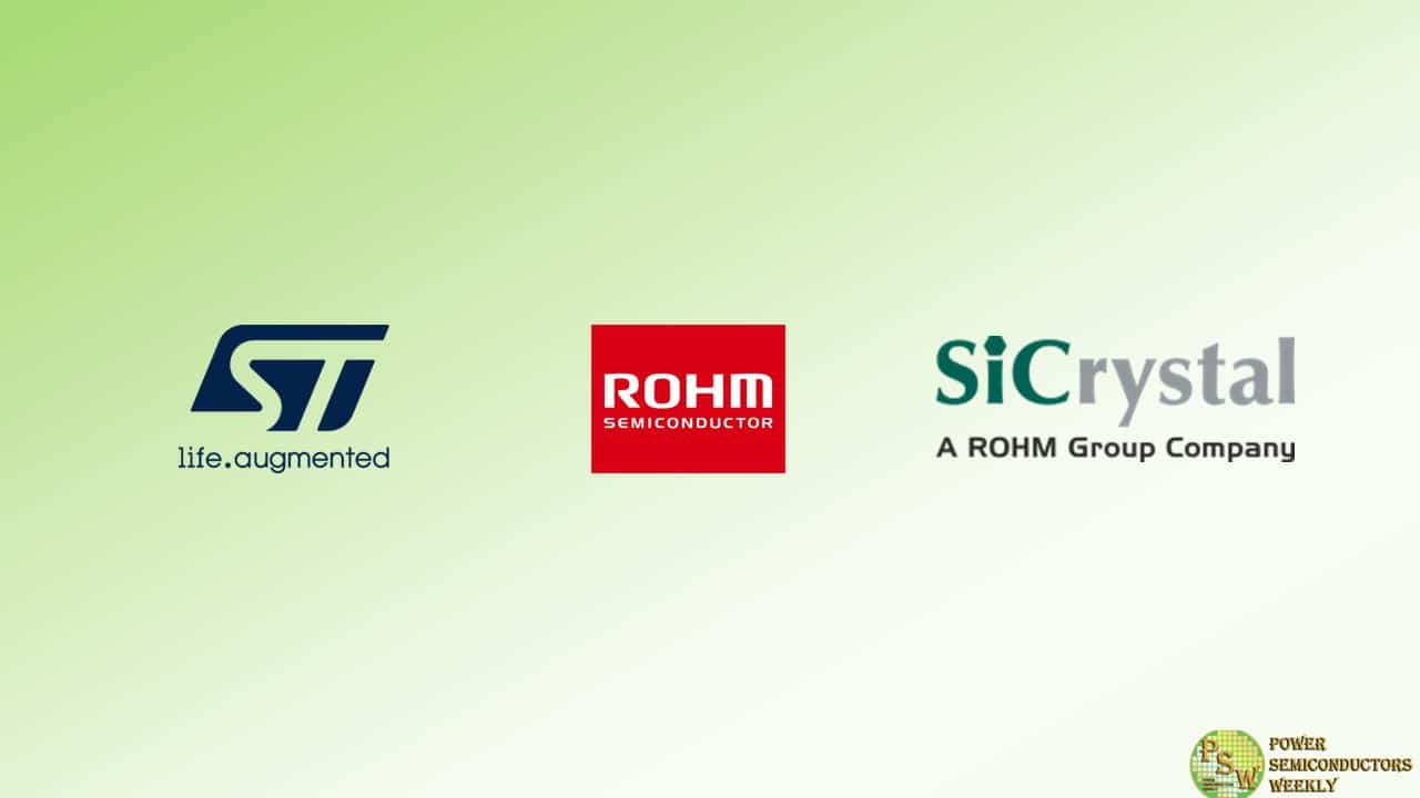
ROHM and STMicroelectronics announced the expansion of the existing multi-year, long-term 150mm silicon carbide (SiC) substrate wafers supply agreement with SiCrystal, a ROHM group company. The new multi-year agreement governs the supply of larger volumes of SiC substrate wafers manufactured in Nuremberg, Germany, for a minimum expected value of $230 million.
Geoff West, EVP and Chief Procurement Officer, STMicroelectronics, commented “This expanded agreement with SiCrystal will bring additional volumes of 150mm SiC substrate wafers to support our devices manufacturing capacity ramp-up for automotive and industrial customers worldwide. It helps strengthen our supply chain resilience for future growth, with a balanced mix of in-house and commercial supply across regions”.
“SiCrystal is a group company of ROHM, a leading company of SiC, and has been manufacturing SiC substrate wafers for many years. We are very pleased to extend this supply agreement with our longstanding customer ST. We will continue to support our partner to expand SiC business by ramping up 150mm SiC substrate wafer quantities continuously and by always providing reliable quality”.said Dr. Robert Eckstein, President and CEO of SiCrystal, a ROHM group company.
Energy-efficient SiC power semiconductors enable electrification in the automotive and industrial sectors in a more sustainable way. By facilitating more efficient energy generation, distribution and storage, SiC supports the transition to cleaner mobility solutions, lower emissions industrial processes and a greener energy future, as well as more reliable power supplies for resource-intensive infrastructure like data centers dedicated to AI applications.
Original – STMicroelectronics
-
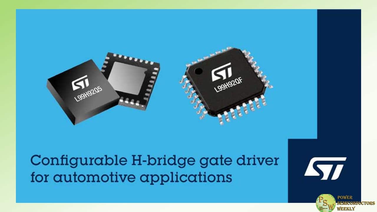
STMicroelectronics unveiled L99H92 automotive gate driver which provides an SPI port for programming and diagnostics, a charge pump, protective features, and two additional current-sense amplifiers for system monitoring.
Containing two high-side and two low-side drivers, the L99H92 can control a single H-bridge powering one bidirectional DC motor or two half bridges for two unidirectional motors. Typical applications for the highly integrated and easily configurable driver include electric sunroof, window lift, powered trunk, sliding doors, and seat-belt pre-tensioners.
The charge pump powers the high-side drivers to maintain correct operation as the vehicle battery voltage fluctuates, enabling the outputs to function with a supply as low as 5.41V. The charge-pump output is also available at an external pin to control a MOSFET for reverse-battery protection.
The gate-driving current is programmed through the SPI port, allowing slew-rate control to minimize electromagnetic emissions and thermal dissipation. Programming the current saves up to four external discrete components per MOSFET, typically needed for slew-rate setting with conventional drivers. The maximum drive current of 170mA gives designers flexibility to use the driver with a wide variety of external MOSFETs, including high-power devices with large gate capacitance.
With many features for system protection and diagnostics, the L99H92 is built for reliability and safety. There is overcurrent protection with a programmable threshold, detected by monitoring the MOSFET drain current. Also, cross-conduction protection with programmable dead time ensures safety and efficiency. Additional protection includes overtemperature early warning and shutdown, overvoltage and undervoltage protection on analog and digital power supply inputs, and open-load and output short-circuit detection in off-state diagnostic mode.
A fail-safe input can turn off all MOSFETs instantaneously and a dedicated diagnostic pin provides immediate fault warning without waiting for periodic SPI transfers.
Additionally, two current-sense amplifiers are integrated for system-status monitoring, helping minimize the bill of materials. Suitable for high-side, low-side, and inline sensing, the amplifiers have independently programmable gain, low offset, and low thermal drift. They can be independently disabled to reduce current consumption when unused.
Original – STMicroelectronics
-
STMicroelectronics released its annual sustainability report, which provides insight into its 2023 performance related to priority environmental, social and governance (ESG) factors that support long-term value creation for all its stakeholders and sustainable growth for its business.
“Sustainability is at the heart of our value proposition, driving benefits for our company, customers, and society. We’re proud of our progress on innovation, resilience, employee engagement and the advancement towards our ambitious goal of becoming carbon neutral on scope 1 and 2, and partially on scope 3, by 2027,” said Jean-Marc Chery, President and CEO, STMicroelectronics. “Together with our partners and empowered employees, we’re accelerating sustainable transformation in technology and beyond.”
ESG highlights during 2023 include:
- A 45% decrease in GHG emissions for scopes 1 and 2 since 2018 in absolute terms (vs a 40% decrease in 2022).
- An increased sourcing of electricity coming from renewable sources to 71% (from 62% in 2022) and the signing of a significant power purchase agreement (PPA) in Italy to produce 250GWh renewable energy per year (3.75 TWh over 15 years) starting in 2024.
- The reuse, recovery, or recycling of 96% of the Company’s waste (1% higher than in 2022).
- A- scores for CDP water security and climate change.
- 12.2% of net revenues (US$2.1 billion) invested in R&D to support innovation.
- Involved in 195 active R&D partnerships worldwide.
- More than 610 STEM (Science, Technology, Engineering, and Mathematics) events and initiatives (a 35% increase on 2022) reaching over 100,000 students and teachers globally.
- 87% of employees would recommend ST as a great place to work, 4% higher than in 2021 (when we last had a full survey).
- In 2023, the company established a strong focus on setting up voluntary, employee-led Employee Resource Groups (ERGs) to promote inclusion in the workplace. WISE (Women Inspiring Supporting and Empowering), the first ERG for women, has grown fast, with some 1,400+ members in 60 locations.
In 2023, ST maintained a strong presence in major sustainability indices such as the Dow Jones Sustainability indices, FTSE4Good, EuroNext VIGEO Europe 120, CAC 40 ESG, MIB ESG, ISS ESG Corporate ratings, Bloomberg Gender Equality Index, and received an MSCI ESG Rating of AAA.
The 27th annual report contains highlights and details of ST’s sustainability performance in 2023 and presents the Company’s ambitions and longer-term goals in alignment with both the United Nations Global Compact Ten Principles and Sustainable Development Goals and the Science Based Targets initiative (SBTi). It is aligned with Global Reporting Standards (GRI), Sustainability Accounting Standards Boards (SASB), and Task Force on Climate-Related Financial Disclosures (TCFD). A third party has verified this report.
More information on ST’s sustainability efforts can be found at https://www.st.com/content/st_com/en/about/sustainability.html
Original – STMicroelectronics
-
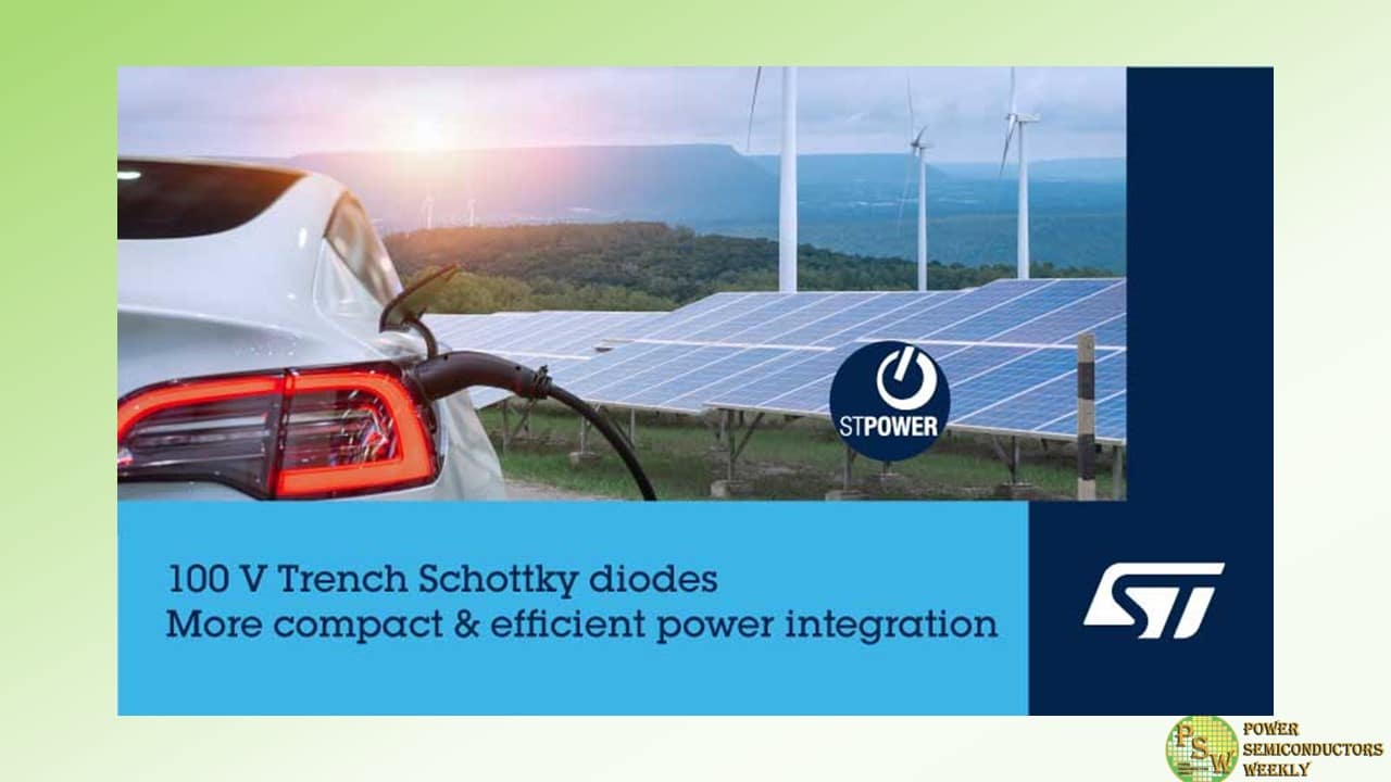
STMicroelectronics introduced 100V trench Schottky rectifier diodes that boost efficiency in power converters operated at high switching frequencies.
Raising power-converter operating frequency, encouraged by the minimal switching losses of technologies like wide-bandgap semiconductors, allows designers to set new benchmarks in power density. However, at elevated frequencies, the energy losses in conventional planar diodes, including silicon Schottky devices, used as rectifiers become a significant factor limiting conversion efficiency.
ST’s trench Schottky diodes significantly reduce the rectifier losses, with superior forward-voltage and reverse-recovery characteristics that enable increased power density with high efficiency. The forward voltage is 50-100mV better than in comparable planar diodes, depending on current and temperature conditions. Simply changing to these devices can increase the efficiency by 0.5%.
There are 28 variants in the new family, with eight current ratings from 1A to 15A, multiple surface-mount packages, in industrial and automotive grades. The industrial-grade parts target applications such as miniature switched-mode power supplies and auxiliary power supplies for telecom, server, and smart-metering equipment.
In automotive, typical uses include space-constrained applications such as LED lighting, reverse-polarity protection, and low-voltage DC/DC converters. The parts are AEC-Q101 qualified, manufactured in PPAP-capable facilities, and specified from -40°C to 175°C.
When combined with ST’s flyback and buck-boost converters, such as the VIPer controllers and HVLED001A offline LED driver, the 100V trench Schottky rectifiers fulfil the active-components bill of materials for switched-mode power supplies. All are supported in ST’s eDesign Suite Rectifier Diodes Simulator, which helps to select the rating and footprint, simulate waveforms, and estimate power efficiency.
The diodes are 100% avalanche tested in production to ensure device robustness and system reliability. They are available in DPAK as well as SOD123 Flat, SOD128 Flat, SMB Flat, and PSMC (TO227A) surface-mount packages.
Original – STMicroelectronics
-
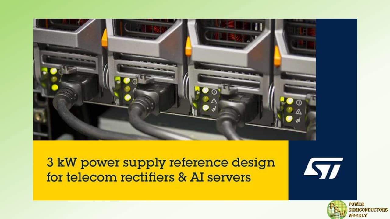
STMicroelectronics announced a collaboration with Compuware Technology Inc, (Compuware), a leading provider of high-efficiency power supplies, on a reference design for server power using ST’s industry-leading silicon carbide (SiC), galvanic isolation, and microcontroller technologies. This reference design provides unparalleled power-supply options for digital power converter applications including server, datacenter and telecom power.
As demand for digital services continues to grow, fueled by Artificial Intelligence (AI), 5G, and the Internet of Things (IoT), keeping power usage under control is an important piece of the sustainability puzzle for data centers. The STDES-3KWTLCP reference design is perfect for a 3kW and higher wattage CRPS (Common Redundancy Power Supply) server power supply. This technical advancement comes with superior efficiency, faster switching, reduced energy losses, and better thermal management capabilities. In addition, this total system solution shortens time-to-market.
Compuware stands as a global power supply leader, holding the world record for the highest number of 80 PLUS Titanium certifications, ensuring unparalleled power efficiency. Engineered for excellence, Compuware power solutions are the ideal choice for HPC, AI, Deep Learning, Cloud, and advanced applications. With high power density, it optimizes space usage without compromising reliability and efficiency, setting a new performance standard in demanding computing environments.
“Combining ST’s latest SiC MOSFET, galvanic isolation, and microcontroller technologies with Compuware’s leading-edge power energy expertise is helping Compuware unleash our design creativity to develop high-density and -efficiency solutions. Now we can achieve 89W/in.3 power density, a small size, and high power output, this reference design is a great choice for power-hungry, high-performance computing applications,” according to Robin Cheng, Vice President at Compuware.
“With a focus on the Industrial market, ST’s Power & Energy Competence Center provides low-power, mid-power, and high-power solutions with the most advanced ST technologies to our customers, and this reference design- STDES-3KWTLCP can help our customers increase energy efficiency and reduce time-to-market using ST’s efficient and reliable power solutions,” said Eric Chou, Head of Power & Energy Competence Center at STMicroelectronics.
Original – STMicroelectronics
