-

Navitas Semiconductor will showcase its latest innovations at the 2024 China Power Electronics and Energy Conversion Conference and the 27th Annual Academic Conference and Exhibition of the China Power Supply Society (CPEEC & CPSSC 2024), held in Xi’an from November 8th – 11th, 2024.
At ‘Planet Navitas’ (Booth 3-011), visitors can discover the AI Power Roadmap, which showcases the world’s first 8.5 kW OCP AI data center power supply implementing GaNSafe and Gen-3 Fast SiC MOSFETs, alongside the highest power density 4.5 kW AI data center power supply on the planet. Navitas also developed the ‘IntelliWeave’ patented digital control combined with high-power GaNSafe™ and Gen 3-Fast SiC MOSFETs, optimized for AI data center power supplies, enabling PFC peak efficiencies to 99.3% and reducing power losses by 30% compared to existing solutions.
Additionally, industry-leading solutions include a 6.6kW 2-in-1 EV on-board charger (OBC) utilizing a hybrid GaNSafe and GeneSiC design and fast-charging solutions for consumer electronics with the latest GaNSlim family.
The new GaNSlim family offers a highly integrated GaN solution with autonomous EMI control and loss-less sensing that enables the industry’s fastest, smallest, and most efficient solution in an optimized DPAK-4L package, ideal for mobile, consumer, and home appliance applications up to 500 W.
Enabled by over 20 years of SiC innovation leadership, GeneSiC technology leads on performance with the Gen-3 Fast SiC MOSFETs with ‘trench-assisted planar’ technology. This proprietary technology provides world-leading performance over temperature, delivering cool-running, fast-switching, and superior robustness to support up to 3x more powerful AI data centers and faster charging EVs.
As China’s premier power electronics event, CPSSC gathers industry leaders, researchers, and enterprises to explore breakthrough technologies shaping the future of power electronics. This year’s focus is on high-efficiency, high-power density solutions. “CPSSC is a key platform to showcase Navitas’ role in advancing power electronics,” said Charles Zha, VP & GM of Navitas China. “Our GaNSafe, GaNSlim, and Gen-3 Fast SiC technologies highlight our commitment to enabling higher efficiency, faster charging, and more powerful applications, aligning with CPSSC’s vision of powering the future.”
Navitas will also present technical papers and host industrial sessions, sharing insights into GaN and SiC technologies and their real-world applications.
Navitas’ CPSSC 2024 Program Highlights:
- November 10
- Paper Presentation:
Research on Parasitic False Turn-On Behaviour of SiC MOSFETs with 0V Turn-Off Gate Voltage
13:20-13:40 | Xiangyang Zhou, Bin Li, Xiucheng Huang, Jason Zhang - Industrial Session:
Bi-Directional GaN for Improving Efficiency in Micro-Inverters
14:30-15:00 | Simon Qin, Sr. Staff Application Engineer
- November 11
- Technical Presentation:
Achieving 99.4% Efficiency in GaN-based Interleaving CrM TTP PFC
08:30-09:00 | Wenhao Yu, Sr. Application Engineer - Technology Showcase:
GaNSlim IC: Redefining Efficiency in Cost-Effective Power Supplies
10:20-10:50 | Ye Hu, Technical Marketing Manager - Industry Insights:
Opportunities and Challenges of Single-Stage Converters for On-Board Chargers
13:00-13:30 | Justin Zhu, Sr. Technical Marketing Manager
Original – Navitas Semiconductor
-

Many industrial applications today are transitioning to higher power levels with minimized power losses, which can be achieved through increased DC link voltage. Infineon Technologies AG addresses this challenge by introducing the CoolSiC™ Schottky diode 2000 V G5, the first discrete silicon carbide diode on the market with a breakdown voltage of 2000 V. The product family is suitable for applications with DC link voltages up to 1500 VDC and offers current ratings from 10 to 80 A. This makes it ideal for higher DC link voltage applications such as in solar and EV charging applications.
The product family comes in a TO-247PLUS-4-HCC package, with 14 mm creepage and 5.4 mm clearance distance. This, together with a current rating of up to 80 A, enables a significantly higher power density. It allows developers to achieve higher power levels in their applications with only half the component count of 1200 V solutions. This simplifies the overall design and enables a smooth transition from multi-level topologies to 2-level topologies.
In addition, the CoolSiC Schottky diode 2000V G5 utilizes the .XT interconnection technology that leads to significantly lower thermal resistance and impedance, enabling better heat management. Furthermore, the robustness against humidity has been demonstrated in HV-H3TRB reliability tests. The diodes exhibit neither reverse recovery current nor forward recovery and feature a low forward voltage, ensuring enhanced system performance.
The 2000 V diode family is a perfect match for the CoolSiC MOSFETs 2000 V in the TO-247Plus-4 HCC package that Infineon introduced in spring 2024. The CoolSiC diodes 2000 V portfolio will be extended by offering them in the TO-247-2 package, which will be available in December 2024. A matching gate driver portfolio is also available for the CoolSiC MOSFETs 2000 V.
Original – Infineon Technologies
-

Electric drives are becoming increasingly prevalent in the boat and ship sector. At METSTRADE, Bosch Engineering is unveiling a newly developed, high-performance electrification solution for electrical systems with voltages of up to 800 volts, which further extends the potential use cases of electric drives in maritime applications while also raising system efficiency.
“With the latest generation of our electric motor and inverter with silicon carbide power modules, we offer a complete system that allows not only recreational boats but also larger sailing yachts and working boats to be operated with an efficient, quiet, yet still very powerful electric drive,” states Philip Kurek, who is responsible for off-highway and maritime solutions at Bosch Engineering.
The new electric motor SMG 230 is designed for system voltages of 400 to 800 volts. In an ideal voltage and temperature range, it offers a continuous power output of up to 200 kilowatts and around 250 newton meters of torque. Thanks to the 800-volt technology, the power density has also been increased significantly. The SMG 230 delivers 80 kilowatts more power than a comparable 400-volt machine with identical weight or, with the same level of performance, boasts more compact dimensions and a much lower weight.
The inverter with silicon carbide semiconductors, which is also designed for electrical voltages of up to 800 volts, is characterized by its impressive efficiency of more than 99 percent. The silicon carbide semiconductors in the power modules enable faster switching operations, meaning that significantly less energy is lost in the form of heat.
Bosch’s complete kit for the electrification of boat drives comprises electronic control units, inverters, electric motors, and transmissions for both 400- and 800-volt applications. This gives shipyards and system integrators maximum flexibility when adapting the electrification strategy to the respective requirements and allows them to integrate the relevant components quickly and easily into their ships. The system components are based on modern automotive technology and combine high robustness with utmost reliability. With its comprehensive kit for the electrification of ship drives, Bosch is making a crucial contribution to the ongoing reduction of greenhouse gas and noise emissions.
Original – Bosch
-

At this month’s IEEE Energy Conversion Congress and Expo (ECCE), Navitas Semiconductor introduced conference attendees to ‘IntelliWeave’ – an innovative patented new digital control technique for improving next generation AI data center power supply (PSU) efficiency.
In a world where ever-more energy is needed for the processing of artificial intelligence (AI) and cloud-based applications, minimizing power consumption has become a priority for data center architects and operators. Combining next-generation GaN and SiC semiconductors with new control technique strategies to power conversion plays a key role in achieving this goal.
IntelliWeave’s novel digital control enables highest system efficiencies with precision current sharing, ultra-fast dynamic response and minimal phase error. A patented dual-loop and dual-feed-forward interleaving control achieves absolute zero voltage switching (ZVS) across the full-load range to enable highest efficiencies.
The digital control for Critical Conduction Mode (CRM) interleaving Totem Pole Power Factor Control (PFC) enables 30% reduction in power losses compared to existing Continuous Conduction Mode (CCM) solutions. The digital control combined with high-power GaNSafe power ICs has been proven on a 500 kHz GaN-based interleaving 3.2 kW CrM PFC PSU operating at 99.3% peak efficiency including EMI filter loss.
Taking place in Phoenix, Arizona from October 20th to 24th, IEEE ECCE 2024 features both industry-driven and application-oriented technical sessions and brings together practicing engineers, researchers and other professionals for interactive and multidisciplinary discussions on the latest advances in various areas related to energy conversion.
On October 21st Tao Wei presented “Novel digital control for a GaN-based CrM interleaved TP PFC”.
Original – Navitas Semiconductor
-

Affordability combined with high performance and efficiency is the key to making electric mobility accessible to a broader market. That’s why Infineon Technologies AG is introducing the HybridPACK™ Drive G2 Fusion, establishing a new power module standard for traction inverters in the e-mobility sector.
The HybridPACK Drive G2 Fusion is the first plug’n’play power module that implements a combination of Infineon’s silicon and silicon carbide (SiC) technologies. This cutting-edge solution provides an ideal balance between performance and cost efficiency, giving more choice in the optimization of inverters.
One of the main differences between silicon and SiC in power modules is that SiC has a higher thermal conductivity, breakdown voltage and switching speed, making it more efficient, but also more expensive than silicon-based power modules. With the new module, the SiC content per vehicle can be reduced, while maintaining vehicle performance and efficiency at a lower system cost. For example, system suppliers can realize nearly the system efficiency of a full SiC solution with only 30 percent SiC and 70 percent silicon area.
“Our new HybridPACK Drive G2 Fusion module underlines Infineon’s innovation leadership in the automotive semiconductor industry,” said Negar Soufi-Amlashi, Senior Vice President & General Manager High Voltage at Infineon’s Automotive division. “Addressing the demand for greater e-mobility range, this technological breakthrough smartly combines silicon carbide and silicon. Integrated in a well-introduced module package footprint it offers compelling cost-performance ratio over pure silicon carbide modules without adding system complexity for automotive system suppliers and vehicle manufacturers.”
HybridPACK Drive G2 Fusion expands Infineon’s HybridPACK Drive power module portfolio and can be quickly and easily integrated in vehicle components or modules without requiring complex adjustments or configurations. The HybridPACK Drive G2 Fusion module features up to 220 kW in the 750 V class. It ensures high reliability over the entire temperature range from -40 °C to +175 °C and improved thermal conductivity.
The unique properties of Infineon’s CoolSiC™ technology and its silicon IGBT EDT3 technology with very fast turn-on enable the use of a single gate driver or dual gate drivers. This allows easy re-design from full silicon or full SiC based inverters to a fusion inverter. Generally, Infineon’s holistic expertise in SiC MOSFET and silicon IGBT technology, power module packaging, gate drivers as well as sensors enables premium products with cost savings at system level. One example is the integration of Swoboda or XENSIV™ Hall sensors in the HybridPACK Drive package for more precise and efficient motor control.
Infineon will showcase the new HybridPACK Drive G2 Fusion at electronica 2024 in Munich from November 12 to 15 (hall C3, booth 502).
Original – Infineon Technologies
-

The U.S. Department of Commerce and Wolfspeed announced they have signed a non-binding preliminary memorandum of terms (PMT) for up to $750 million in proposed direct funding under the CHIPS and Science Act. In addition, a consortium of investment funds led by Apollo, The Baupost Group, Fidelity Management & Research Company and Capital Group have agreed to provide Wolfspeed an additional $750 million of new financing.
Together these investments support Wolfspeed’s long-term growth plans and bolster domestic production of silicon carbide to power clean energy systems underpinning electric vehicles (EVs), artificial intelligence (AI) data centers, battery storage and more. In addition, Wolfspeed expects to receive $1 billion of cash tax refunds from the advanced manufacturing tax credit under the CHIPS and Science Act (section 48D), giving the company, in total, access to up to $2.5 billion of expected capital to support the expansion of silicon carbide manufacturing in the United States.
Wolfspeed is the world’s largest producer of silicon carbide technology, pioneering the technology more than 35 years ago on the campus of North Carolina State University. Since that time, Wolfspeed has become the global leader in silicon carbide technology, one of the fastest growing components of the broader semiconductor industry.
- Silicon carbide is a superior alternative to silicon for high power applications – such as EV powertrains, e-mobility, renewable energy systems, battery energy storage systems, and AI and cryptocurrency data centers – that unlocks improved performance and lower system costs.
- Notably, the importance of bolstering the domestic production of silicon carbide has been recognized across multiple federal agencies; the Department of Energy denoted it as one of 17 “critical materials” with a high risk of supply disruption that are integral to clean energy technologies, while the Department of Commerce recognizes silicon carbide semiconductors as important to national security.
- As the U.S. and the world pursue more efficient and environmentally friendly solutions to meet the world’s ever-increasing need for high-voltage energy products, it is crucial that the U.S. continue to make strategic investments to cement its technological leadership position, while continuing to spur American innovation in critical technologies.
Wolfspeed CEO, Gregg Lowe, said, “To reach this milestone under the U.S. CHIPS and Science Act is an incredible achievement in Wolfspeed’s long-term growth strategy, and we believe today’s announcement is a testament to the market-leading quality of Wolfspeed products and significance of Wolfspeed to broader U.S. economic and national security interests. This support galvanizes our ability to expand domestic manufacturing, accelerate innovation in next-generation semiconductor technology, and meet the increasing global demand for silicon carbide. As a key player in the semiconductor industry, this proposed investment will enable us to solidify our leadership position with a first-of-its-kind 200mm silicon carbide manufacturing footprint in upstate New York and central North Carolina, while contributing to the resilience and competitiveness of the U.S. supply chain. It’s not just about growth for Wolfspeed—it’s about driving technological advancement that powers the future.
“Silicon carbide is already enabling superior energy efficiency across mission-critical industries of the future like electric vehicles, e-mobility, solar and wind energy, industrial power applications, and AI data centers. While EVs have been the driver of silicon carbide adoption thus far, we believe the use cases for our technology are expansive and will only continue to grow as more and more industries find themselves needing to solve for the same power loss, system size, and system cost challenges as automakers,” concluded Lowe.
“Artificial intelligence, electric vehicles, and clean energy are all technologies that will define the 21st century, and thanks to proposed investments in companies like Wolfspeed, the Biden-Harris Administration is taking a meaningful step towards reigniting U.S. manufacturing of the chips that underpin these important technologies,” said U.S. Secretary of Commerce Gina Raimondo. “Because of the Biden-Harris Administration’s CHIPS and Science Act, the United States is building and fortifying our semiconductor manufacturing capabilities to serve our economic and national security interests while creating jobs and economic opportunities for communities across the country.”
“Wolfspeed is leading the pack in bringing semiconductor manufacturing back to America. This major multibillion dollar investment powered by my CHIPS & Science Law will accelerate the ongoing expansion in the Mohawk Valley, helping speed up hiring of hundreds of new good-paying jobs that Wolfspeed is creating in the Mohawk Valley and providing long term work for the Marcy fab to succeed well into the future, further establishing Upstate NY as a global hub for chip manufacturing,” said Senator Chuck Schumer. “From electric vehicles to artificial intelligence, this critical technology relies on the silicon carbide chips that Wolfspeed will manufacture and perfect in the Mohawk Valley. Today’s massive investment will make America’s economy and our national security stronger as Wolfspeed helps us write the next chapter of America’s resurgence as the leader in the semiconductor industry, with the Mohawk Valley as the beating heart.”
“Wolfspeed is a homegrown semiconductor innovator and manufacturer creating great jobs in North Carolina, and it’s important they received this major grant under the CHIPS and Science Act,” said North Carolina Governor Roy Cooper. “Thanks to this landmark legislation from the Biden-Harris Administration and our great workforce, we will continue to see good paying jobs coming to North Carolina.”
“This $750 million federal investment is a testament to Wolfspeed’s unique leadership in silicon carbide semiconductor manufacturing, and I applaud Wolfspeed’s continued commitment to North Carolina,” said Senator Thom Tillis. “I was proud to vote for the CHIPS and Science Act to provide the funding for this investment in North Carolina and to support our economic and national security.”
“North Carolina continues to be a leader in cutting-edge manufacturing that is vital to our country’s national and economic security,” said Senator Ted Budd. “This new Wolfspeed site in Siler City will bring good-paying jobs to the area and is an important first step in making sure America has secure supply chains for critical semi-conductors.”
“We are pleased to expand our investment in Wolfspeed by providing additional capital in support of the company’s build out of its leading silicon carbide capabilities,” said Apollo Partner Joseph Jackson. “We believe Wolfspeed is at the forefront of a critical transformation in sustainable transportation and ensuring that the company has durable capital access to complete its expansion plans will help solidify its leadership in this space. Along with our lending consortium, which includes multiple funds that also own substantial equity stakes in the company, we believe this strategic investment will drive significant long-term value while advancing key tenets of the CHIPS and Science Act.”
These proposed funds, which are expected to be received upon milestone achievements in the coming years, would enable Wolfspeed to complete its multi-billion-dollar greenfield U.S. capacity expansion plan, which consists of the largest and most advanced 200mm silicon carbide footprint in the world. In addition to the proposed direct funding, Wolfspeed intends to benefit from the U.S. Treasury Department Investment Tax Credit of up to 25% of the qualified capital expenditures primarily related to its construction and installation of equipment at The John Palmour Manufacturing Center for Silicon Carbide in Siler City, NC and completion of the Mohawk Valley Fab M-Line West Expansion in Utica, NY.
This multi-billion-dollar investment will bolster Wolfspeed’s balance sheet and will help to fuel significant growth through cash generation and accelerate its long-term profitability goals.
Summary of the PMT
The PMT outlines key terms for a CHIPS incentive award, including the proposed amount and form of the award, and provides that the disbursement of funds will be conditioned upon the achievement of certain operational and construction milestones and other requirements.
The PMT includes an obligation for Wolfspeed to raise an aggregate of $750 million in debt financing over three tranches through the issuance of senior notes under an amended and restated indenture. Wolfspeed and its lenders, led by Apollo funds, have reached an agreement for this additional financing, including $250 million to be available within 10 business days, and have agreed to certain intercreditor terms with the CHIPS Program Office as described in the PMT.
Together, the PMT and the agreement with lenders also requires:
- Wolfspeed to undertake further actions with respect to its capital structure, including (a) restructuring or refinancing its outstanding 2026, 2028 and 2029 convertible notes at specified intervals prior to their respective maturity dates, (b) deferring a total of $120 million in cash interest payments due prior to June 30, 2025 under an unsecured customer refundable deposit agreement, and (c) raising up to $300 million of additional capital from non-debt sources over the next 12 months.
- In addition, Wolfspeed has agreed with its lenders to certain revisions in the terms of the senior notes, including revisions to the interest rate applicable to the senior notes, as described in the Form 8-K filed today with Securities and Exchange Commission (SEC).
The PMT provides that the award is subject to due diligence and the negotiation and signing of a definitive direct funding agreement with the Department of Commerce and the negotiation and signing of an intercreditor agreement between the Department of Commerce and the Company’s lenders, which may contain different or additional conditions not contained in the PMT. Additional terms of the PMT were not disclosed.
Original – Wolfspeed
-

CISSOID announced that its SiC Inverter Control Module (ICM) has been adopted by Hydro Leduc, a renowned manufacturer of hydraulic components, for its new highly efficient and modular Electric Power Take-Off (ePTO). This new ePTO solution supports the electrification of trucks and other off-road vehicles. CISSOID’s ICM not only powers and controls Hydro Leduc’s compact and efficient inverter but also contributed to greatly accelerate its development cycle.
Hydro Leduc’s new ePTO solution offers an optimized hydraulic supply to high power tools in e-trucks and other off-road vehicles that remain driven by hydraulic actuators. Hydro Leduc’s new ePTO represents a significant advancement in electric and hydraulic transmissions with their ME230, a 76 kW brushless electric motor designed to be paired with an inverter for applications up to 650Vdc.
This motor, compatible with DIN ISO14 standards and equipped with an efficient cooling system, forms a complete solution with the new series of fixed displacement spherical piston pumps: the XRe, available in 41 or 63 cm³ displacements.
Specially adapted for E-PTO mounting, the XRe series is quiet and offers remarkable efficiency, reduced pulsations due to its 9-piston design, and high speed in self-priming mode. Together, the ME230 and XRe provide high-performance and efficient electro-hydraulic solutions for a variety of applications.
CISSOID’s ICM optimally integrates a 3-Phase 1200V/340A-550A SiC Power Module, enabling efficient power conversion, a gate driver board designed for safe driving of the fast-switching SiC transistors, and a control board embedding a powerful real-time microprocessor. This hardware platform has been delivered together with the OLEA® APP INVERTER software optimized for the efficient and safe control of electric motors.
Olivier Savinois, Managing Director at EL MOTION (the sister company of Hydro Leduc, specialized in the design and manufacturing of electrical components and motors), said “We have been very pleased to work with CISSOID on the development of our new ePTO inverter. Not only did their SiC Inverter Control Module completely match our needs, we also enjoyed outstanding support from their team. Especially due to the on-site calibration of our inverter and motor, during the design and validation phases. CISSOID’s modular inverter platform ties perfectly with our scalable ePTO solution.”
Emmanuel Poli, VP Sales at CISSOID, said: “It was really exciting to work with the Hydro Leduc team, who rapidly understood how powerful it would be to leverage our ICM to accelerate the design of their inverter. We were impressed by the speed and agility of Hydro Leduc’s engineers in integrating our hardware and software solution into their motor drive.”
Original – CISSOID
-
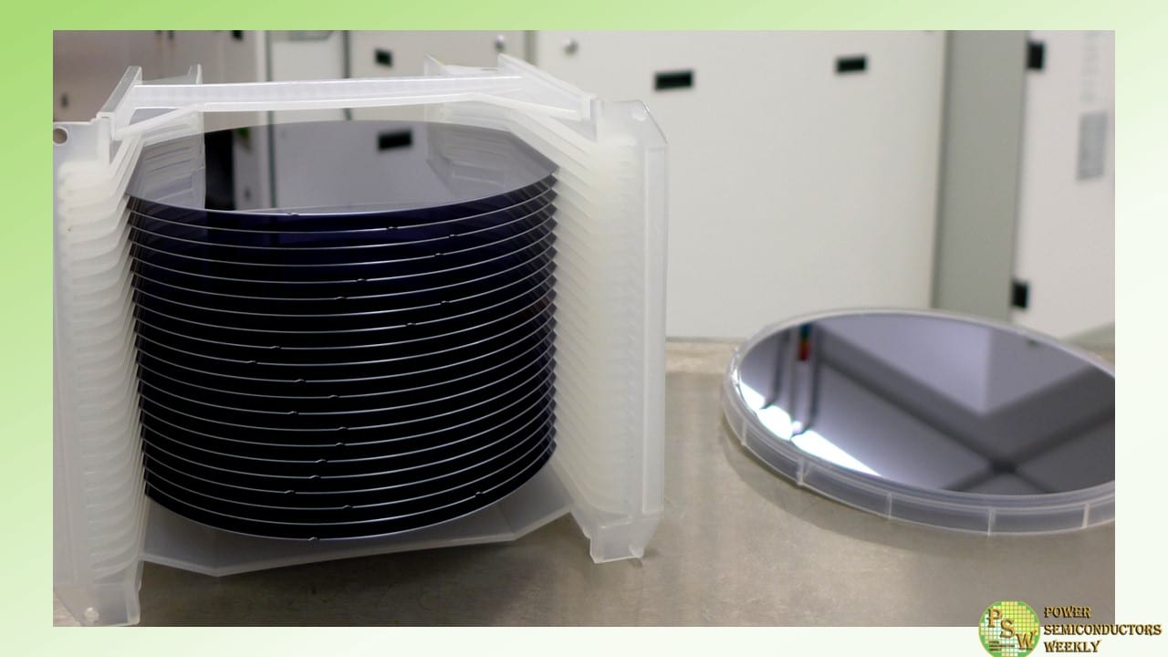
Coherent Corp. announced the launch of its 200 mm silicon carbide epitaxial wafers. Substrate and epi-wafer shipments from the company at 350 micron and 500 micron thickness are now underway.
As a dedicated manufacturer of both SiC substrates and epitaxial wafers, Coherent combines these elements to deliver exceptional quality, performance, and reliability. The new 200 mm SiC epi-wafers are engineered with cutting-edge thickness and doping uniformity, setting new industry standards and supporting the production of superior SiC power semiconductors.
“With our advanced technology, we are not only enhancing the quality of SiC devices but also addressing the growing demand for 200 mm for efficient power-conversion components in critical sectors,” said Gary Ruland, Vice President and General Manager of the SiC Materials Business Unit.
SiC devices are integral to power conversion in electric and hybrid vehicles, energy infrastructure, and high-power EV chargers. The transition from 150 mm to 200 mm diameter wafers responds to the increasing demand for SiC semiconductors, allowing manufacturers to produce more devices per wafer. This shift is expected to enhance productivity and reduce the cost of SiC devices, benefiting a wide range of applications.
By adopting larger wafers, SiC device manufacturers can achieve higher yields and improved cost efficiency because of a 1.8x increase in usable area per wafer. The implementation of state-of-the-art 200 mm tooling brings additional advantages while aligning with the industry’s drive for greater performance and reduced operational costs.
Original – Coherent
-
 LATEST NEWS / PRODUCT & TECHNOLOGY / SiC / WBG
Axus Technology Introduced Industry’s Lowest Cost of Ownership for CMP Processes on 200mm SiC Wafers
September 26, 2024
2 Min ReadAxus Technology, a leading global provider of chemical mechanical planarization (CMP) equipment, critical for semiconductor and compound semiconductor fabrication, announced its flagship CapstoneÆ CS200 platform tools offer the industry’s lowest cost of ownership (CoO) for CMP processes on 200mm silicon carbide (SiC) wafers. Compared to its closest competitor, Axus’s small-footprint Capstone delivers twice the throughput at less than half the total cost per wafer.
Yole Group forecasts the overall SiC manufacturing tool market to top US$4.4 billion by 2029. “The unique properties of SiC require specialized manufacturing tools and lines for processing power SiC devices,” the market analyst firm noted earlier this year. Axus anticipated this need, designing the state-of-the-art Capstone from the ground up to deliver advanced processing capabilities for SiC in power electronics and other applications.
“Many 200mm fabs are looking to upgrade their installed base of CMP tools to products with leading-edge capability and functionality. Our ability to deliver industry-low CoO further underscores our strong market position and capacity to support this shift,” said Axus Technology CEO Dan Trojan. “Capstone features a streamlined workflow and integrated cleaning capability, so it requires half the process steps of older CMP tools. This allows customers to greatly lower their capex investment.”
Key Capstone CoO advantages vs. competitor
- Throughput: 2.5x wafers per hour
- Power consumption: 60% lower
- DI water consumption: 80% lower
- Footprint: 45% smaller
- Capex cost per wafer: 65% lower
- Total cost per wafer: 50% lower
Another factor contributing to Capstone’s lower CoO is its built-in Process Temperature Control (PTC) technology, which enables processing at higher pressures and speeds without exceeding temperature limits of polishing pads and other sensitive components. This feature is vital for SiC and other materials with high hardness and planarization challenges that necessitate more aggressive process conditions.
Axus built its proprietary CoO model using its own system specifications, publicly available specs for competitive tools, actual consumables costs, and real-world performance data supplied by customers. The comprehensive model factors in all CoO contributors: process variables (polish time and removal rates), polishing and cleaning consumables, power and deionized (DI) water usage, system footprint, and equipment capex including cost, utilization and wafer capacity.
Original – Axus Technology
-
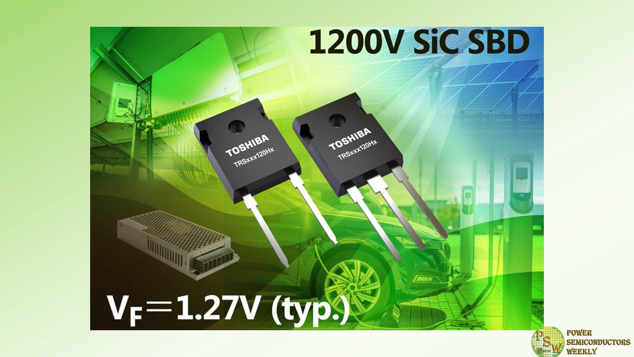
Toshiba Electronics Europe GmbH enhances its silicon carbide (SiC) diode portfolio with ten new 1200V Schottky barrier diodes (SBDs). The TRSxxx120Hx series, comprising five products housed in TO-247-2L packages and five in TO-247 packages, helps designers improve the efficiency of industrial equipment, including photovoltaic (PV) inverters, electric vehicle (EV) charging stations, and switching power supplies.
By implementing an enhanced junction barrier Schottky (JBS) structure, the TRSxxx120Hx series allows a very low forward voltage (VF) of just 1.27V (typ.). The merged PiN-Schottky incorporated into a JBS structure reduces diode losses under high current conditions. The TRS40N120H of the new series accepts a forward DC current (IF(DC)) of 40A (max) and a non-repetitive peak forward surge current (IFSM) of 270A (max), with the maximum case temperature (TC) of all devices being +175°C.
Combined with the lower capacitive charge and leakage current, the products help improve system efficiency and simplify thermal design. For instance, at a reverse voltage (VR) of 1200V, the TRS20H120H diode housed in the TO-247-2L package provides a total capacitive charge (QC) of 109nC and reverse current (IR) of 2µA.
Original – Toshiba
