-

onsemi has signed a multi-year deal with Volkswagen Group to be the primary supplier of a complete power box solution as part of its next-generation traction inverter for its Scalable Systems Platform (SSP). The solution features silicon carbide-based technologies in an integrated module that can scale across all power levels – from high power to low power traction inverters to be compatible for all vehicle categories.
“By offering a complete power system solution that encompasses the entire power sub-assembly, we provide Volkswagen Group with a single, simplified modular and scalable platform that maximizes efficiency and performance for their vehicle lineup,” said Hassane El-Khoury, president and CEO of onsemi. “This new approach allows for the customization of power needs and the addition of features for different vehicles without compromising on performance, all while reducing cost.”
Based on the EliteSiC M3e MOSFETs, onsemi’s unique power box solution can handle more power in a smaller package which significantly reduces energy losses. The inclusion of three integrated half-bridge modules mounted on a cooling channel will further improve system efficiency by ensuring heat is effectively managed from the semiconductor to the coolant encasement.
This leads to better performance, improved heat control, and increased efficiency, allowing EVs to drive further on a single charge. By using this integrated solution, Volkswagen Group will be able to easily transition to future EliteSiC-based platforms and remain at the forefront of EV innovation.
“We are very pleased to have onsemi as a strategic supplier for the power box of the traction inverter for our first tranche in the SSP platform. onsemi has convinced us with a deeply verticalized supply chain from the growth of the raw material up to the assembly of the power box,” said Mr. Dirk Große-Loheide, Member of the Extended Executive Committee Group Procurement and Member of the Board Volkswagen Brand for “Procurement”.
Mr. Till von Bothmer, Senior Vice President VW Group Procurement for Powertrain added, “On top of the verticalization, onsemi has furthermore provided a resilient supply concept with regional silicon carbide fabs across Asia, Europe and the U.S. In addition, onsemi will continuously provide the latest SiC generation to ensure competitiveness.
Volkswagen Group will also benefit from onsemi’s planned investment to expand its silicon carbide manufacturing in the Czech Republic. The investment would establish an end-to-end production facility in Europe for the traction inverter power system. The proximity of onsemi’s facility would fortify Volkswagen Group’s supply chain while improving logistics and allowing for faster integration into the manufacturing process.
Original – onsemi
-

In the face of escalating climate crises and a dramatic rise in global energy demands, governments and industries are committing to ambitious climate goals aimed at mitigating environmental impact and securing a sustainable future. Key to these efforts is the transition to electrification to reduce carbon emissions and embrace renewable energy resources.
In a significant step towards accelerating this global transition, onsemi introduced its latest generation silicon carbide technology platform, EliteSiC M3e MOSFETs. The company also disclosed plans to release multiple additional generations through 2030.
“The future of electrification is dependent on advanced power semiconductors. Today’s infrastructure cannot keep up with the world’s demands for more intelligence and electrified mobility without significant innovations in power. This is critical to the ability to achieve global electrification and stop climate change,” said Simon Keeton, group president, Power Solutions Group, onsemi. “We are setting the pace for innovation, with plans to significantly increase power density in our silicon carbide technology roadmap through 2030 to be able to meet the growing demands for energy and enable the global transition to electrification.”
The EliteSiC M3e MOSFETs will play a fundamental role in enabling the performance and reliability of next-generation electrical systems at lower cost per kW, thus influencing the adoption and effectiveness of electrification initiatives. With the ability to operate at higher switching frequencies and voltages while minimizing power conversion losses, this platform is essential for a wide range of automotive and industrial applications such as electric vehicle powertrains, DC fast chargers, solar inverters and energy storage solutions.
Additionally, the EliteSiC M3e MOSFETs will enable the transition to more efficient, higher-power data centers to meet the exponentially increasing energy demands that power a sustainable artificial intelligence engine.
Through onsemi’s unique design engineering and manufacturing capabilities, the EliteSiC M3e MOSFETs achieve a significant reduction in both conduction and switching losses on the trusted and field-proven planar architecture. Compared to previous generations, the platform can reduce conduction losses by 30% and turn-off losses by up to 50%.
By extending the life of SiC planar MOSFETs and delivering industry-leading performance with EliteSiC M3e technology, onsemi can ensure the robustness and stability of the platform, making it a preferred choice for critical electrification applications
The EliteSiC M3e MOSFETs also offer the industry’s lowest specific on-resistance (RSP) with short circuit capability which is critical for the traction inverter market that dominates SiC volume. Packaged in onsemi’s state-of-the-art discrete and power modules, the 1200V M3e die delivers substantially more phase current than previous EliteSiC technology, resulting in approximately 20% more output power in the same traction inverter housing. Conversely, a fixed power level can now be designed with 20% less SiC content, saving costs while enabling the design of smaller, lighter and more reliable systems.
Additionally, onsemi provides a broader portfolio of intelligent power technologies including gate drivers, DC-DC converters, e-Fuses and more to pair with the EliteSiC M3e platform. The end-end onsemi combination of optimized, co-engineered power switches, drivers and controllers enable advanced features via integration, lowering overall system cost.
Global energy demands are projected to soar over the next decade, making the need for increased power density in semiconductors paramount. onsemi is leading innovation across its silicon carbide roadmap – from die architectures to novel packaging techniques – that will continue to address the general industry demand for increased power density.
With each new generation of silicon carbide, cell structures will be optimized to efficiently push more current through a smaller area, increasing power density. When coupled with the company’s advanced packaging techniques, onsemi will be able to maximize performance and reduce package size.
By applying the concepts of Moore’s Law to the development of silicon carbide, onsemi can develop multiple generations in parallel and accelerate its roadmap to bring several new EliteSiC products to market at an accelerated pace through 2030.
“We are applying our decades of experience in power semiconductors to push the boundaries of speed and innovation in our engineering and manufacturing capabilities to meet the rising global energy demands,” said Dr. Mrinal Das, senior director of technical marketing, Power Solutions Group, onsemi. “There is a huge technical interdependency between the materials, device and package in silicon carbide. Having full ownership over these key aspects allows us to have control over the design and manufacturing process and bring new generations to market much faster.”
The EliteSiC M3e MOSFET in the industry-standard TO-247-4L package is now sampling.
Original – onsemi
-

Electrification, renewables and artificial intelligence are global megatrends converging and driving unprecedented demands for advanced power semiconductors capable of optimizing energy conversion and management. In a strategic move toward addressing these demands, onsemi announced plans to establish a state-of-the-art, vertically integrated silicon carbide (SiC) manufacturing facility in the Czech Republic. The site would produce the company’s intelligent power semiconductors that are essential for improving the energy efficiency of applications in electric vehicles, renewable energy and AI data centers.
“Our brownfield investment would establish a Central European supply chain to better service our customers’ rapidly increasing demand for innovative technologies that improve the energy efficiency in their applications,” said Hassane El-Khoury, president and CEO, onsemi. “Through a close collaboration with the Czech government, the expansion would also enhance our production of intelligent power semiconductors that are essential to helping ensure the European Union is able to achieve its ambitions to significantly reduce carbon emissions and environmental impact.”
“onsemi’s decision to expand in Czechia is a clear confirmation of our country’s attractiveness for foreign investment and will bring significant momentum for the development of our economy,” said Mr. Jozef Síkela, Minister of Industry and Trade of the Czech Republic. “This investment not only strengthens our position in the semiconductor field but can also contribute to the development of the automotive industry and help us with its adaptation to the rise of electromobility.”
onsemi’s plan to expand SiC manufacturing with a multi-year brownfield investment of up to $2 billion (44 billion CZK) is part of the company’s previously disclosed long-term capital expenditure target. This investment would build on the company’s current operations in the Czech Republic, which include silicon crystal growth, silicon and silicon carbide wafer manufacturing (polished and EPI) and a silicon wafer fab. Today, the site can produce more than three million wafers annually, including more than one billion power devices. Upon completion, the operation would contribute annually more than $270 million USD (6 billion CZK) to the country’s GDP.
Pending all final regulatory and incentive approvals, including the investment incentive approval by the government of the Czech Republic and its notification to the European Commission, this would be one of the largest private sector investments in the Czech Republic’s history and would further contribute to the prosperity and economic dynamism of the Zlín region. onsemi is one of the first companies to invest in advanced semiconductor manufacturing in the Central European region.
With this investment, the company would contribute to the strategic positioning of the region within the EU’s semiconductor value chain and demonstrate that all EU countries can benefit from the European Chips Act. The announcement also reflects onsemi’s strategic alignment with the overarching goals of the European Chips Act of increasing market share and technological advancement to strengthen the resilience of the EU’s semiconductor supply chains in times of ever-growing demand.
Silicon carbide is a critical material for high-power, high-temperature applications, and is extremely difficult to produce. onsemi is one of the only companies in the world with the ability to manufacture SiC-based semiconductors from crystal growth to advanced packaging solutions. By expanding its production facilities in the Czech Republic, onsemi would be faster to provide supply assurance for customers, strengthening its leadership in intelligent power solutions. This integration would also enable onsemi to leverage its latest advancements in research and development (R&D) to maximize manufacturing and production efficiency.
Original – onsemi
-
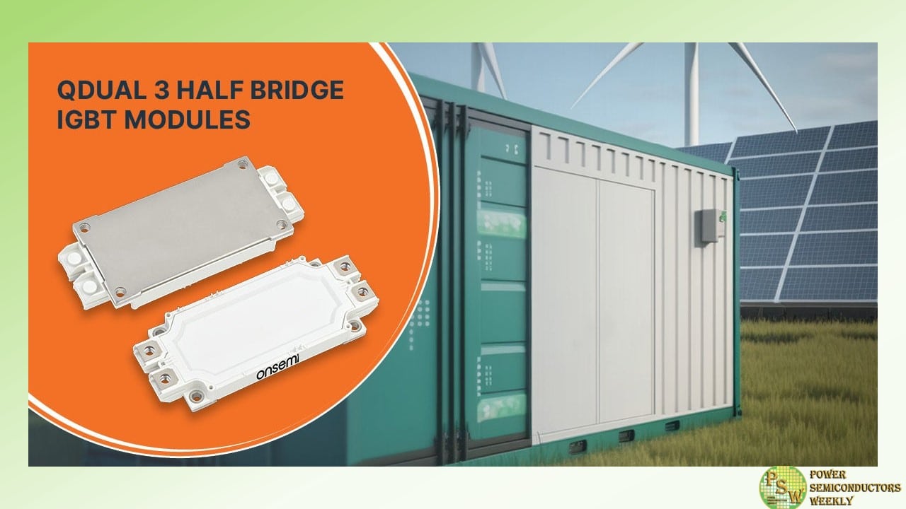
The latest onsemi 7th generation 1200V QDual3 Insulated Gate Bipolar Transistor (IGBT) power modules offer increased power density and deliver up to 10% more output power than other available competing products. Based on the latest Field Stop 7 (FS7) IGBT technology, the 800-amp (A) QDual3 module delivers industry-leading efficiency to reduce system costs and simplify designs.
In a 150KW inverter, the QDual3 module will dissipate 200 watts (W) less in losses compared to the closest competition, significantly reducing heatsink size. QDual3 is engineered to work under harsh conditions and is ideal for high-power electronics converters such as central inverters in solar farms, energy storage systems (ESS), commercial agricultural vehicles (CAVs) and industrial motor drives.
Currently, two products are available depending on the applications – NXH800H120L7QDSG and SNXH800H120L7QDSG.
Increasing renewable energy adoption amplifies the need for solutions that can manage peak demand and ensure continuous power supply. Peak shaving, the practice of reducing electricity use during peak hours, is essential for maintaining electric grid stability and reducing costs. Using the QDual3 modules, manufacturers can construct a solar inverter and ESS that output more power in the same system size, enabling more efficient energy management and storage capabilities, and allowing for a smoother integration of solar power into the grid.
The modules also mitigate the intermittency of solar energy by storing excess power in an ESS, ensuring a reliable and consistent energy flow. For large systems, the modules can be paralleled to increase the output power up to a couple of MWs and compared to traditional 600 A module solutions, the 800 A QDual3 significantly reduces the module quantity, greatly simplifying design complexity and cutting system costs.
The QDual3 IGBTs module features an 800 A half-bridge configuration that integrates the latest Gen7 trench Field Stop IGBT and diode technology using onsemi’s advanced packaging techniques to reduce switching and conduction losses.
With FS7 technology, the die size is reduced by 30%, allowing more die per module, increasing the power density to enable the maximum current capacity up to 800 A or higher. With an IGBT Vce(sat) as low as 1.75V (175°C) and low Eoff, the 800 A QDual3 module dissipates 10% lower energy losses than the next-best alternative. The modules also meet the stringent standards required of an automotive application.
“Increased electrification of commercial fleets such as trucks and busses and the need of renewable energy sources demand solutions that can generate, store and distribute power more efficiently. Transferring energy from renewable sources to the grid, storage systems and to downstream loads with the lowest power losses possible is increasingly critical,” said Sravan Vanaparthy, vice president, Industrial Power Division, Power Solutions Group, onsemi. “With its industry-standard pin-out and market-leading efficiencies, QDual3 enables power electronics designers to plug and play these modules for an immediate performance boost in their systems.”
Original – onsemi
-

As data centers become increasingly power-hungry to support the tremendous processing requirements of AI workloads, the need for boosting energy efficiency is paramount. The powerful combination of onsemi’s latest generation T10 PowerTrench® family and EliteSiC 650V MOSFETs create a solution that offers unparalleled efficiency and high thermal performance in a smaller footprint for data center applications.
Compared to a typical search engine request, an AI-supported engine request requires more than 10x the power, leading to data center power needs expected to reach an estimated 1,000 TWh globally in less than two years. To process one AI-supported request, energy is converted four times from the grid to the processor, which can result in an energy loss of approximately 12%.
Using the T10 PowerTrench family and EliteSiC 650V solution, data centers are able to reduce power losses that occur by an estimated 1%. If implemented in data centers globally, the solution could reduce energy consumption by 10 TWh annually or the equivalent of the energy required to fully power nearly one million homes per year.
The EliteSiC 650V MOSFET offers superior switching performance and lower device capacitances to achieve higher efficiency in data centers and energy storage systems. Compared to the previous generation, these new generation silicon carbide (SiC) MOSFETs have halved the gate charge and reduced both the energy stored in output capacitance (Eoss) and the output charge (Qoss) by 44%.
With no tail current during turn-off and superior performance at high temperatures, they can also significantly reduce switching losses compared to super junction (SJ) MOSFETs. This allows customers to downsize system components while increasing the operating frequency, resulting in an overall reduction in system costs.
Separately, the T10 PowerTrench Family is engineered to handle high currents, crucial for DC-DC power conversion stages, and offers increased power density and superior thermal performance in a compact footprint. This is achieved through a shield gate trench design, which boasts an ultra-low gate charge and an RDS (on) of less than 1 milliohm. Additionally, the soft recovery body diode and lower Qrr effectively minimizes ringing, overshoots, and electrical noise to ensure optimal performance, reliability, and robustness under stress. The T10 PowerTrench Family also meets the stringent standards required for automotive applications.
The combined solution also meets the stringent Open Rack V3 (ORV3) base specification required by hyperscale operators to support the next generation of high-power processors.
“AI and electrification are reshaping our world and skyrocketing power demands. Accelerating innovation in power semiconductors to improve energy efficiency is key to enabling these technological megatrends. This is how we power the future responsibly,” said Simon Keeton, group president, Power Solutions Group, onsemi. “Our latest solution can significantly reduce power losses that occur during the energy conversion process and have a meaningful impact on the demands for the next generation of data centers.”
Original – onsemi
-

onsemi announced results for the first quarter of 2024 with the following highlights:
- Revenue of $1,862.7 million
- GAAP gross margin and non-GAAP gross margin of 45.8% and 45.9%, respectively
- GAAP operating margin and non-GAAP operating margin of 28.2% and 29.0%, respectively
- GAAP diluted earnings per share and non-GAAP diluted earnings per share of $1.04 and $1.08, respectively
- Returned ~100% of free cash flow over last twelve months to shareholders through stock repurchases
“The structural changes we have made to the business over the last three years have enabled us to sustain our gross margin despite challenging market conditions,” said Hassane El-Khoury, president and chief executive officer of onsemi. “In the current environment, we remain focused on execution while investing for our long-term growth. As power continues to play a critical role in the world’s increasing energy demands, efficiency is paramount, and we are positioned to continue to gain share with our portfolio of industry-leading power and sensing technologies.”
Selected financial results for the quarter are shown below with comparable periods (unaudited):
GAAP Non-GAAP (Revenue and Net Income in millions) Q1 2024 Q4 2023 Q1 2023 Q1 2024 Q4 2023 Q1 2023 Revenue $ 1,862.7 $ 2,018.1 $ 1,959.7 $ 1,862.7 $ 2,018.1 $ 1,959.7 Gross Margin 45.8 % 46.7 % 46.8 % 45.9 % 46.7 % 46.8 % Operating Margin 28.2 % 30.3 % 28.8 % 29.0 % 31.6 % 32.2 % Net Income attributable to ON Semiconductor Corporation $ 453.0 $ 562.7 $ 461.7 $ 464.5 $ 540.9 $ 523.7 Diluted Earnings Per Share $ 1.04 $ 1.28 $ 1.03 $ 1.08 $ 1.25 $ 1.19 Revenue Summary (in millions) (Unaudited) Three Months Ended Business Segment(1) Q1 2024 Q4 2023 Q1 2023 Sequential Change Year-over-Year Change PSG $ 874.2 $ 965.5 $ 860.9 (9 )% 2 % AMG 697.0 744.9 744.7 (6 )% (6 )% ISG 291.5 307.7 354.1 (5 )% (18 )% Total $ 1,862.7 $ 2,018.1 $ 1,959.7 (8 )% (5 )% (1) During the first quarter of 2024, the Company reorganized certain reporting units and its segment reporting structure. As a result of the reorganization of divisions within PSG and AMG, the prior-period amounts have been reclassified to conform to current-period presentation. SECOND QUARTER 2024 OUTLOOK
The following table outlines onsemi’s projected second quarter of 2024 GAAP and non-GAAP outlook.
Total onsemiGAAP SpecialItems Total onsemiNon-GAAP Revenue $1,680 to $1,780 million – $1,680 to $1,780 million Gross Margin 44.1% to 46.1% 0.1% 44.2% to 46.2% Operating Expenses $327 to $342 million $14 million $313 to $328 million Other Income and Expense (including interest), net ($12 million) – ($12 million) Diluted Earnings Per Share $0.82 to $0.94 $0.04 $0.86 to $0.98 Diluted Shares Outstanding 436 million 4 million 432 million Original – onsemi
-

onsemi announced the formation of the Analog and Mixed-Signal Group (AMG) which will be led by newly appointed group president, Sudhir Gopalswamy. The group will be focused on expanding onsemi’s portfolio of industry-leading power management and sensor interface devices to unlock an additional $19.3 billion total addressable market and accelerate the company’s growth in the automotive, industrial and cloud end markets.
Additionally, Simon Keeton has been promoted to group president of the Power Solutions Group (PSG). His leadership has been instrumental in delivering more than $4 billion in total revenue last year, while ramping a profitable silicon carbide business that achieved over $800 million in revenue in 2023.
“This organizational alignment builds on our strength in delivering highly differentiated and optimized solutions focused on customer needs,” said Hassane El-Khoury, president and chief executive officer of onsemi. “With Simon and Sudhir’s industry expertise and proven track records, we are setting the foundation for further growth and leadership in intelligent power and sensing technologies.”
AMG specializes in the development of a range of power management ICs and high precision, low power sensor interfaces and communications products. It positions onsemi to become a full suite provider of high efficiency power tree solutions with an expanded portfolio of gate drivers, DC-DC converters, multi-phase controllers, eFuses and more.
The group will continue to extend its leadership in automotive- and industrial-focused sensor interface and communication solutions such as inductive, ultrasonic and medical sensing, as well as single-pair Ethernet and Bluetooth® Low Energy (Bluetooth LE) solutions.
AMG combines the former Advanced Solutions Group (ASG) and Integrated Circuits Division (ICD), previously a part of PSG. Gopalswamy will oversee both AMG and Intelligent Sensing Group (ISG), which together drove nearly $4 billion in revenue for the company last year.
This strategic move accelerates onsemi’s position and will add even more system value for customers by powering every architecture with analog and mixed-signal technologies that enable advanced functionality, higher performance and faster time to market.
onsemi will publish its first quarter 2024 earnings based on the reorganized business segments and provide comparable historical data.
Original – onsemi
-
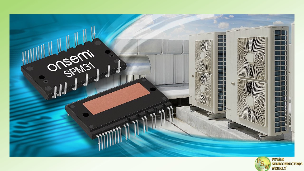
onsemi announced the availability of its 1200V SPM31 Intelligent Power Modules (IPMs) featuring the latest generation Field Stop 7 (FS7) Insulated Gate Bipolar Transistor (IGBT) technology. The SPM31 IPMs deliver higher efficiency, smaller footprint and higher power density resulting in lower total system cost than other leading solutions on the market.
Given the greater efficiency realized using optimized IGBTs, these IPMs are ideal for three-phase inverter drive applications such as heat pumps, commercial HVAC systems, servo motors, and industrial pumps and fans.
Operating residential and commercial buildings is estimated to contribute 26% of greenhouse gas emissions, with indirect emissions such as heating, cooling and powering buildings accounting for approximately 18%. As governments worldwide strive to meet their energy and climate commitments, more energy-efficient and lower-carbon solutions are becoming increasingly critical.
The SPM31 IPMs control the power flow to the inverter compressor and fans in heat pumps and air conditioning systems by adjusting the frequency and voltage of the power supplied to three-phase motors for maximum efficiency. For example, onsemi’s 25A-rated SPM31 using FS7 IGBT technology can decrease power losses by up to 10% and increase in power density up to 9%, compared to our previous generation products.
With the transition to electrification and heightened efficiency mandates, these modules help manufacturers drastically improve system design while increasing efficiency in heating and cooling applications. With the improved performance, our SPM31 IPM family featuring FS7 enables high efficiency with reduced energy losses, further reducing harmful emissions globally.
These highly integrated modules contain gate-driving ICs, multiple on-module protection features along with our FS7 IGBTs enabling industry-leading thermal performance with the ability to support a wide range of currents, from 15A to 35A. With their best-in-class power density, SPM31 FS7 IGBT IPMs are an ideal answer to save mounting space and improve performance expectations while shortening the development time. In addition, the SPM31 IPMs include the following benefits:
- Controls for gate drivers and protections
- Low loss, short-circuit-rated IGBTs
- Negative IGBT terminals available for each phase to support a wide variety of control algorithms
- Built-in under-voltage protection (UVP)
- Built-in bootstrap diodes and resistors
- Built-in high-speed high-voltage integrated circuit
- Single-grounded power supply
Original – onsemi
-

onsemi announced its fourth quarter and fiscal year 2023 results with the following highlights:
- Fourth quarter revenue of $2,018.1 million
- Fourth quarter GAAP and non-GAAP gross margin of 46.7%
- GAAP operating margin and non-GAAP operating margin of 30.3% and 31.6%, respectively
- GAAP diluted earnings per share and non-GAAP diluted earnings per share of $1.28 and $1.25, respectively
- Full year 2023 record automotive revenue of $4.3 billion increased 29% year-over-year
- Full year 2023 share repurchases of $564 million, representing 140% of free cash flow
“Our momentum continued this past year as we achieved record automotive revenue and 4x year-over-year growth in silicon carbide revenue. We continue to transform the business by building resilience into our model, enabling us to navigate uncertain market conditions and deliver more predictable and sustainable results,” said Hassane El-Khoury, president and chief executive officer of onsemi.
“Our consistent performance has validated our long-term strategy. Looking ahead, we are driving innovation beyond silicon and silicon carbide with our upcoming analog and mixed signal platform to further our leadership in intelligent power and sensing solutions.”
Original – onsemi
-
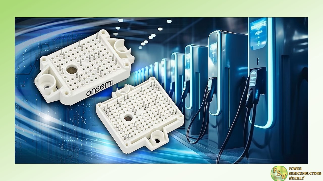
onsemi announced the availability of nine new EliteSiC Power Integrated Modules (PIMs) enabling bidirectional charging capabilities for DC ultra-fast electric vehicle (EV) chargers and energy storage systems (ESS). The silicon carbide-based solutions will dramatically improve system cost with higher efficiency and simpler cooling mechanisms that can reduce size by up to 40% and weight by up to 52% compared to traditional silicon-based IGBT solutions.
With more compact, lighter charging platforms, designers will have all the key building blocks that are needed to quickly deploy a reliable, efficient and scalable network of DC fast chargers that can charge electric vehicle batteries up to 80% in as little as 15 minutes.
According to J.D. Power’s 2023 Electric Vehicle Consideration Study, nearly half of U.S. consumers note the reason for not purchasing an electric vehicle is the access to charging and the ability to do so quickly, to ensure the driving experience is as easy and seamless as with a traditional internal combustion engine (ICE) vehicle. In the U.S., the availability of EV chargers needs to quadruple by 2025 and 8x by the end of the decade to keep up with demand and ensure drivers have equitable access to public charging stations.
In turn, this rapid increase in demand for electricity will also put a tremendous strain on current electrical grids, potentially overloading them. To mitigate this problem, bidirectional charging has emerged as a key solution to implement vehicle-to-grid which allows both regular battery charging and the ability to use an EV as an energy storage system to power your home when needed.
This solution helps enable a DC fast charging network and vehicle-to-grid power transfer systems, addressing access and speed with its ability to recharge a vehicle faster than other methods that take hours or even days.
onsemi offers the most comprehensive portfolio of PIMs to address the key topologies on the market. This gives designers the flexibility to pick the right PIM for power conversion stages in their DC fast charging or energy storage system applications. To accelerate the design cycle, advanced piecewise linear electrical circuit simulation (PLECS) models through our Self-Service PLECS model Generator and application simulation with the Elite Power Simulator of this portfolio will also be made available to designers.
For each module, onsemi uses die from the same wafer to ensure more consistency and reliability so designers don’t have to use discretes from different suppliers, which can lead to varying performance results. In addition to its reliability, this module portfolio offers the following benefits:
- Uses the Gen3 M3S SiC MOSFET technology which offers the lowest switching losses and highest efficiency in the industry
- Supports key topologies such as multi-level T-type neutral point clamp (TNPC), half-bridge and full-bridge topologies
- Supports scalable output power from 25 kW to 100 kW, enabling multiple DC fast charging and energy storage systems platforms including bidirectional charging
- Industry-standard F1 and F2 packages with the option of pre-applied Thermal Interface Material (TIM) and press fit pins
- Enables optimal thermal management, avoiding system failure due to overheating
- Full SiC modules offer energy conservation by minimizing power losses, directly translating to cost and energy savings
- Offers more robustness and dependability, ensuring consistent operations
Original – onsemi
