-
Navitas Semiconductor released its 4.5 kW AI data center power supply reference design, with optimized GaNSafe™ and Gen-3 ‘Fast’ (G3F) SiC power components. The optimized design enables the world’s highest power density with 137 W/in3 and over 97% efficiency.
Next-generation AI GPUs like NVIDIA’s Blackwell B100 and B200 each demand over 1 kW of power for high-power computation, 3x higher than traditional CPUs. These new demands are driving power-per-rack specifications from 30-40 kW up to 100 kW.
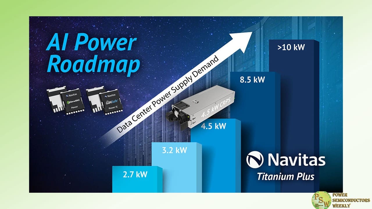
Navitas announced its AI Power Roadmap in March 2024, showcasing next-generation data center power solutions for the growing demand in AI and high-performance computing (HPC) systems. The first design was a GaNFast-based 3.2 kW AC-DC converter in the Common Redundant Power Supply (CRPS) form factor, as defined by the hyperscale Open Compute Project. The 3.2 kW CRPS185 (for 185 mm length) enabled a 40% size reduction vs. the equivalent legacy silicon approach and easily exceeded the ‘Titanium Plus’ efficiency benchmark, critical for data center operating models and a requirement for European data center regulations.
Now, the latest 4.5 kW CRPS185 design demonstrates how new GaNSafe™ power ICs and GeneSiC Gen-3 ‘Fast’ (G3F) MOSFETs enables the world’s highest power density and efficiency solution. At the heart of the design is an interleaved CCM totem-pole PFC using SiC with full-bridge LLC topology with GaN, where the fundamental strengths of each semiconductor technology are exploited for the highest frequency, coolest operation, optimized reliability and robustness, and highest power density and efficiency. The 650 V G3F SiC MOSFETs feature ‘trench-assisted planar’ technology which delivers world-leading performance over temperature for the highest system efficiency and reliability in real-world applications.
For the LLC stage, 650 V GaNSafe power ICs are ideal and unique in the industry with integrated power, protection, control, and drive in an easy-to-use, robust, thermally-adept TOLL power package. Additionally, GaNSafe power ICs offer extremely low switching losses, with a transient-voltage capability up to 800 V, and other high-speed advantages such as low gate charge (Qg), output capacitance (COSS), and no reverse-recovery loss (Qrr). High-speed switching reduces the size, weight, and cost of passive components in a power supply, such as transformers, capacitors, and EMI filters. As power density increases, next-gen GaN and SiC enable sustainability benefits, specifically CO2 reductions due to system efficiency increases and ‘dematerialization’.
The 3.2 kW and 4.5 kW platforms have already generated significant market interest with over 30 data center customer projects in development expected to drive millions in GaN and SiC revenue, ramping from 2024 into 2025.
Navitas’ AI data center power supply reference designs dramatically accelerate customer developments, minimize time-to-market, and set new industry benchmarks in energy efficiency, power density and system cost, enabled by GaNFast power ICs and GeneSiC MOSFETs. These system platforms include complete design collateral with fully tested hardware, embedded software, schematics, bills-of-material, layout, simulation, and hardware test results.
“AI is dramatically accelerating power requirements of data centers, processors and anywhere AI is going in the decades to come creating a significant challenge for our industry. Our system design center has stepped up to this challenge delivering a 3x increase in power in less than 18 months”, said Gene Sheridan, CEO of Navitas Semiconductor. “Our latest GaNFast technology, combined with our G3F SiC technology are delivering the highest power density and efficiency the world has ever seen…the perfect solution for the Blackwell AI processors and beyond.”
Original – Navitas Semiconductor
-
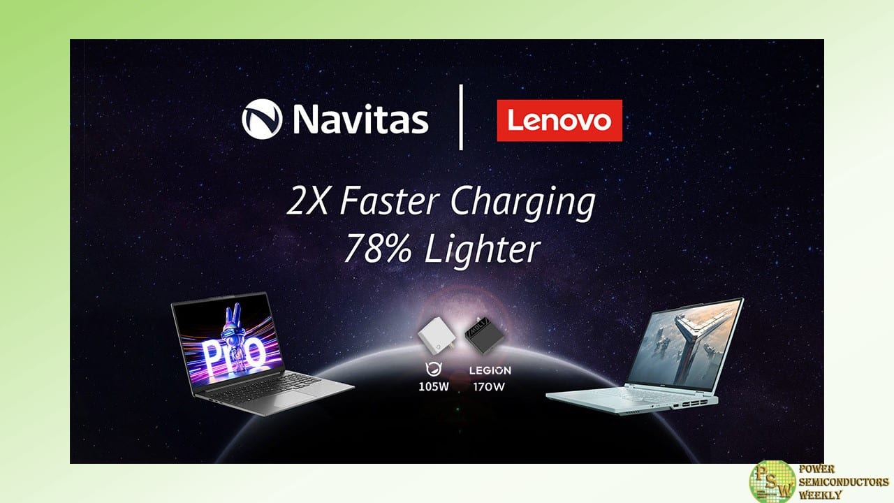
Navitas Semiconductor announced that its GaNFast power ICs have been selected to lead Lenovo’s latest GaN technology chargers; Xiaoxin 105 W GaN charger, and the Legion C 170 W GaN charger, respectively designed for daily travel and gaming power, bringing consumers a brand new fast charging experience.
The Xiaoxin 105 W GaN charger is designed for daily travel. It outputs 105 W of power and is equipped with 3 ports (2C1A) supporting multiple protocols; easily achieving the charging needs of various devices simultaneously. At only 206 g, the 105 W fast-charger is 41% lighter than a typical 100 W computer adapter and takes only 34 minutes to charge the Xiaoxin 16 Pro to 50%. The Navitas NV6138 GaNFast power IC with GaNSense™ technology is at the heart of the high-frequency flyback topology design, providing a stable, durable, and efficient charging experience.
The Legion C170 W GaN charger is designed specifically for hardcore gamers. It delivers 170 W of continuous power through a single port to meet the high-power demands of gaming devices. At only 245 grams, it’s 78% lighter than Legion Y9000P’s original inbox charger and can charge up to 2 times faster than the Legion C140 W Charger. The Navitas NV6136 GaNFast power IC with GaNSense technology is used in the PFC stage, featuring loss-less current sensing and 6 times faster short-circuit protection than competing solutions, delivering cooler operation, superior efficiency, reliability, and power density.
Lenovo’s long-term collaboration with Navitas has brought a series of groundbreaking fast chargers to the market and played a significant role in raising market awareness on showcasing the benefits of GaN technology. At the Lenovo YOGA CC65 dual-port GaN charger launch event in 2021, Navitas’ 6-inch GaN wafer and GaNFast power ICs were publicly showcased for the first time, unveiling the mysteries of this leading technology to consumers.
In terms of gaming products, Navitas collaborated with Lenovo to create a 90 W charger for the Lenovo Legion Pro Gaming Phone and a 135 W, C135 W GaN charger for the Legion 5 and 5 Pro Gen 7 laptops. For lightweight travel, Lenovo developed a series of compact, lightweight powerful GaN chargers using Navitas technology, including the revolutionary compact Thinkplus ‘lipstick’ and the ultra-thin Thinkbook ‘biscuit’ charger.
Lenovo and Navitas are not only partners in power technology but also pioneers in sustainability. Lenovo Group is verified by the Science Based Targets initiative (SBTi) for net zero targets and Navitas is the world’s first power semiconductor company to achieve CarbonNeutral® certification. Navitas’ advanced GaN technology enables Lenovo to continuously create smaller, lighter chargers with higher power density, significantly reducing the number of passive and magnetic components inside the charger, achieving CO2 reduction in production through “dematerialization”. The increased efficiency reduces power loss during use, thus further lowering carbon emissions in the product lifecycle.
“With the support of Navitas GaNFast power ICs, we have successfully introduced two new Xiaoxin and Legion GaN chargers to the market, enabling a lightweight and powerful charging experience for daily travel and gaming performance,” said Elon Chen, Product Manager of Consumer Business for Lenovo Group China. “Moreover, the successful application of Navitas’ GaNFast technology continuously reduces the size and weight of chargers, highly increasing efficiency, bringing convenience to consumers, while contributing to carbon reduction.”
“Powerland is very pleased to collaborate with Navitas again to create two high-performance and lightweight GaN chargers for Lenovo,” said Dr. Wang Chuanyun, VP of R&D for Powerland Group. “Powerland is dedicated to pushing the envelope of technology to build leading power products for our clients. Efficient, reliable, and easy-to-use GaNFast power ICs are crucial to realize that.”
“Navitas is very honored to enter Lenovo’s supply chain twice in a short period, providing high-efficiency and stable GaNFast fast charging power into two important Lenovo products,” said Charles Zha, VP and GM of Navitas China. “By working closely with Powerland, our highly integrated GaNFast technology has enabled Lenovo to continuously achieve leading-edge results in size, performance, and reliability of chargers. With innovative laptops like AI PCs on the rise, Navitas predicts a surge in demand for powerful GaNFast charging solutions. Navitas is on a mission to push the limits of gallium nitride technology, empowering global partners like Lenovo to slash energy usage and emissions in charger and adapter production. Together, we will speed towards a greener, more sustainable planet!”
Original – Navitas Semiconductor
-
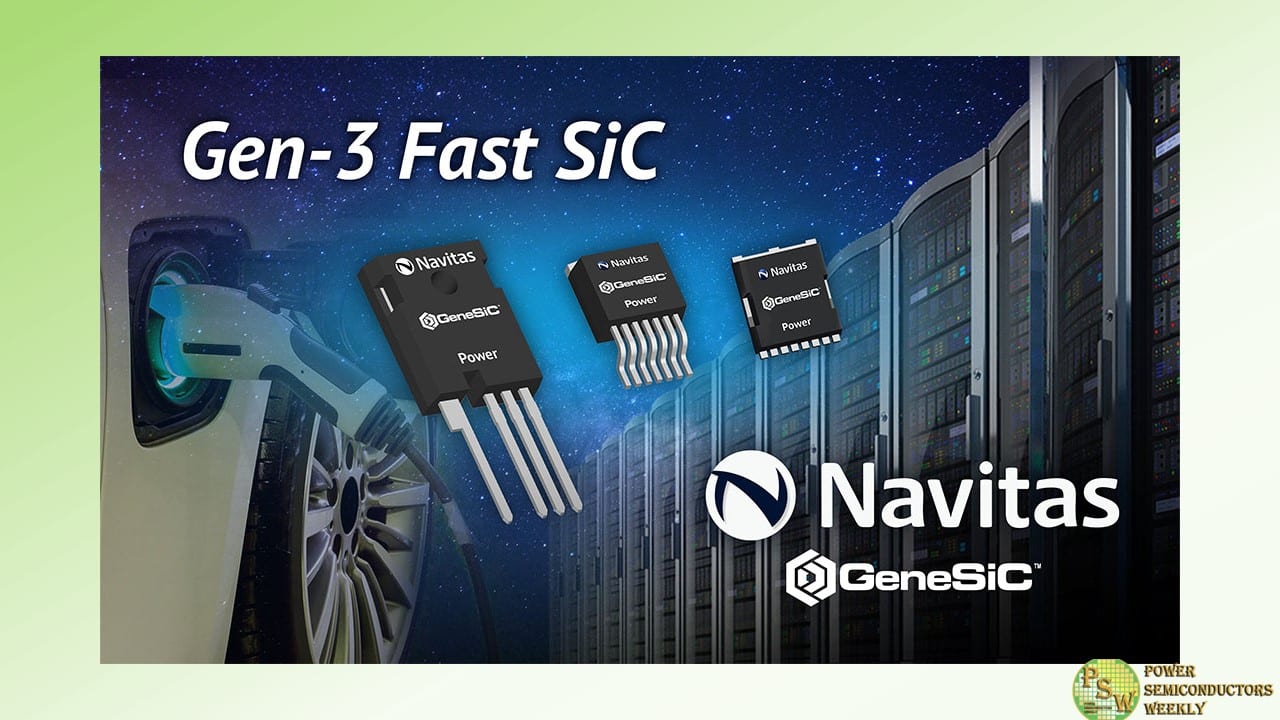
Navitas Semiconductor announced their new portfolio of Gen-3 ‘Fast’ (G3F) 650 V and 1,200 V SiC MOSFETs optimized for fastest switching speed, highest efficiency, and increased power density for applications such as AI data center power supplies, on-board chargers (OBCs), fast EV roadside super-chargers, and solar / energy-storage systems (ESS). The broad portfolio range covers industry-standard packages from D2PAK-7 to TO-247-4, designed for demanding, high-power, high-reliability applications.
The G3F family is optimized for high-speed switching performance, resulting in 40% improvement to hard-switching figures-of-merits (FOMs) compared to competition in CCM TPPFC systems. This will enable increasing the wattage of next-generation AI power supply units (PSUs) up to 10 kW, and power per rack increase from 30 kW to 100-120 kW.
The G3F GeneSiC MOSFETs are developed using a proprietary ‘trench-assisted planar’ technology. and offer better-than-trench MOSFET performance, while also providing superior robustness, manufacturability and cost than competition. G3F MOSFETs deliver high-efficiency with high-speed performance, enabling up to 25°C lower case temperature, and up to 3x longer life than SiC products from other vendors.
The ‘trench-assisted planar’ technology enables an extremely low RDS(ON) increase versus temperature, which results in the lowest power losses across the complete operating range and offers up to 20% lower RDS(ON) under real-life operation at high temperatures compared to competition.
Additionally, all GeneSiC MOSFETs have the highest-published 100%-tested avalanche capability, 30% longer short-circuit withstand time, and tight threshold voltage distributions for easy paralleling, GeneSiC MOSFETs are ideal for high-power, fast-time-to-market applications.
Navitas’ latest 4.5 kW high-power density AI Server PSU reference design in CRPS185 form-factor, showcases the 650 V-rated, 40mOhms G3F FETs for an Interleaved CCM TP PFC topology. Alongside the GaNSafe™ Power ICs in the LLC stage, a power density of 138 W/inch3 and peak efficiency above 97% is realized, which comfortably achieves ‘Titanium Plus’ efficiency standards, now mandatory in Europe.
For the EV market, 1,200 V/34 mOhm (G3F34MT12K) G3F FETs enable Navitas’ new 22 kW, 800V Bi-Directional OBC and 3KW DC-DC converter to achieve a superior power density of 3,5 kW/L and a peak efficiency of 95.5%.
“G3F sets a new standard for efficient, cool-running SiC performance, coupled with high reliability and robustness for high-power, high-stress systems,” noted Dr. Sid Sundaresan, Senior Vice President of SiC Technology and Operations. “We’re pushing the boundaries of SiC, with up to 600 kHz switching speeds, and hard-switching figures-of-merit up to 40% better than competition.”
Original – Navitas Semiconductor
-
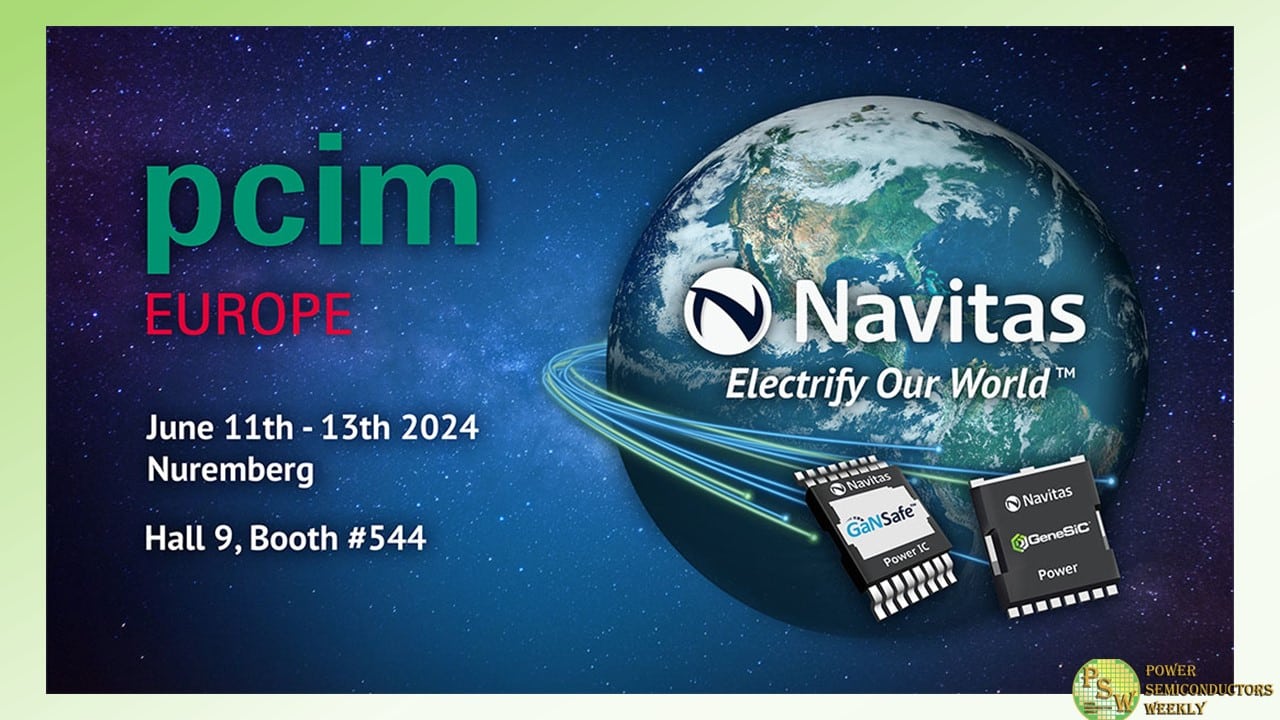
Navitas Semiconductor invites visitors to experience “Planet Navitas” at PCIM 2024 (June 11th-13th) and see how industry-leading GaN and SiC solutions deliver optimal performance in a broad array of fast-growing markets and applications from 20 W to 20 MW.
Aligned with Navitas’ mission to “Electrify Our World™”, the “Planet Navitas” booth invites visitors to discover how next-gen GaN and SiC technology enable the latest solutions for fully-electrified EV transportation, AI data centers, industrial compressors, drives, and robotics plus renewable energy sourcing and storage.
Each example highlights end-user benefits such as increased portability, longer range, faster charging, and grid independence, along with a focus on how low-carbon-footprint GaN and SiC technology can save over 6 Gtons/yr CO2 by 2050.
“PCIM is a key event in the power-electronics calendar,” says Alessandro Squeri, Navitas’ senior director for European sales. “Complementary GaNFast and GeneSiC portfolios, with comprehensive, application-specific system design support, accelerate customer time-to-market with sustainable performance advantages. ‘Planet Navitas’ represents the very real, inspiring implementation of GaN & SiC that makes up a $1.6B identified customer pipeline as part of a vast $22B/year market opportunity.”
Major technology updates and releases include GaNSafe™ – the world’s most-protected, most reliable, and highest-performance GaN power, Gen-4 GaNSense™ Half-Bridge ICs – the most integrated GaN devices, and Gen-3 Fast GeneSiC power FETs – for game-changing motor drive and energy-storage applications.
In addition to the exhibition, PCIM 2024 includes peer-review technical presentations, including:
11th June, 13:00 – 14:30, Hall 10.1
- “Low-Cost High-Density 300 W / 20 V AC-DC Converter Enabled by GaN Power ICs”– Tom Ribarich, Sr. Director of Strategic Marketing, Navitas Semiconductor
- A low-cost 300 W high-density AC-to-DC converter has been designed and demonstrated to achieve >96% peak efficiency and 270 cc. The circuit topologies include a 2-phase interleaved PFC input stage, an LLC DC-DC stage, and a synchronous rectification output stage. The design includes GaN Power ICs and off-the-shelf controllers running at 300 kHz. This new design has resulted in a cased power density of 1.1 W/cc.
12th June, 15:30 – 17:00, Foyer
- Evaluation of SiC Devices for Over 500 kHz Application Based on Buck Circuit – Minli Jia, Sr. Staff Applications Engineer, Navitas Semiconductor
- This paper selects three 1200 V SiC devices of similar specifications and different manufacturers for analysis and experimental research and designs a Buck converter with an output power of 3.6 kW and a switching frequency of 600 kHz. The efficiency and heat of three SiC types were tested under the same working conditions, and the results showed that the SiC with fast turn-off characteristics and low thermal resistance was more suitable for high-frequency converter applications.
Original – Navitas Semiconductor
- “Low-Cost High-Density 300 W / 20 V AC-DC Converter Enabled by GaN Power ICs”– Tom Ribarich, Sr. Director of Strategic Marketing, Navitas Semiconductor
-
Navitas Semiconductor announced unaudited financial results for the first quarter ended March 31, 2024.
“I am very pleased with our first quarter revenue growth of over 70% from the prior year, despite an overall market slowdown,” said Gene Sheridan, CEO and co-founder. “Response to our latest technologies – GaNSafe™, Gen-3 Fast GeneSiC™ and now GaNSlim technology – has been impressive. Our customer pipeline – which has grown to $1.6 billion – shows that future demand for electrification and energy savings is stronger than ever.”
1Q24 Financial Highlights
- Revenue: Total revenue grew to $23.2 million in the first quarter of 2024, a 73% increase from $13.4 million in the first quarter of 2023.
- Loss from Operations: GAAP loss from operations for the quarter was $31.6 million, compared to a loss of $35.5 million for the first quarter of 2023. On a non-GAAP basis, loss from operations for the quarter was $11.8 million compared to a loss of $12.3 million for the first quarter of 2023.
- Cash: Cash and cash equivalents were $129.7 million as of March 31, 2024.
Market, Customer and Technology Highlights
- AI Data Center: Leading-edge GaNSafe and Gen-3 Fast GeneSiC technologies with unique system design-center solutions enable 3x increase in power capability to support AI-based data centers. Announcing 3 major design wins at the world’s largest power-supply companies, in combination with over 30 customer projects in development. In the coming quarters, we expect to power data centers at AWS, Azure, Google, Supermicro, Inspur and Baidu.
- EV: New 22 kW on-board charger (OBC) platform delivers up to 3x faster charging, 2x power density, 30% greater energy savings and 40% lighter weight relative to current solutions. Now engaged with over 160 EV-related customers across all major regions and increased total pipeline by over 50% since the $400 million reported in December.
- Solar / Energy Storage: Won 6 new designs across US, Europe and Asia for solar optimizers, micro-inverters, string inverters and energy-storage applications for 2025 ramp, with significant increase in pipeline.
- Home Appliance / Industrial: Latest, motor-optimized GaNSense™ half-bridge power ICs in over 15 customer developments. Gen-3 Fast GeneSiC and GaNSafe technologies are achieving rapid industrial adoption with over 25 customer developments.
- Mobile / Consumer: Over 20 new fast chargers added in the last quarter, taking the total released customer products to over 450, across all 10 of the top 10 mobile OEMs. New gen-4 GaN IC projects include Xiaomi launching another two smartphone models (Mi 14 Ultra and the CIVI 4Pro) to support ultra-fast charging, and Lenovo with the ThinkBook 170W desktop 5-port charger and docking station.
Business Outlook
- Second quarter 2024 net revenues are expected to be $20 million plus or minus $500 thousand. Non-GAAP gross margin for the second quarter is expected to be 40% plus or minus 50 basis points and non-GAAP operating expenses are expected to be approximately $21.5 million in the second quarter of 2024.
Original – Navitas Semiconductor
-

Ernst & Young LLP (EY US) announced that Gene Sheridan, CEO and co-founder of Navitas Semiconductor was named an Entrepreneur Of The Year® 2024 Greater Los Angeles Award finalist. Now in its 38th year, ‘Entrepreneur Of The Year’ is the preeminent competitive business award for audacious leaders who disrupt markets, revolutionize sectors and have a transformational impact on lives. Over the past four decades, the program has recognized daring entrepreneurs with big ideas and bold actions that reshape our world.
Mr. Sheridan was selected as a finalist by an independent panel of judges, and evaluated based on demonstration of building long-term value through entrepreneurial spirit, purpose, growth and impact, among other core contributions and attributes.
“We are at a pivotal time in our planet’s energy transformation, and this recognition from EY highlights the importance of Navitas’ mission to ‘Electrify Our World’ and exploit a $1.3T opportunity as we accelerate the transition from fossil fuels to renewable energy,” said Mr. Sheridan. “Next-generation gallium nitride (GaN) and silicon carbide (SiC) power semiconductors enable fast, efficient and sustainable ultra-fast charging and power delivery in AI datacenters, advanced EVs, mobile, solar and industrial applications. EY’s recognition is a significant moment, a motivation and recognition for me and all of the contributors who have made Navitas a great company.”
Entrepreneur Of The Year honors many different types of business leaders for their ingenuity, courage and entrepreneurial spirit. The program celebrates original founders who bootstrapped their business from inception or who raised outside capital to grow their company; transformational CEOs who infused innovation into an existing organization to catapult its trajectory; and multigenerational family business leaders who reimagined a legacy business model to fortify it for the future.
Regional award winners will be announced on June 13, 2024 during a special celebration at The Beverly Hills Hotel and will become lifetime members of an esteemed community of Entrepreneur Of The Year alumni from around the world. The winners will then be considered by the National judges for the Entrepreneur Of The Year National Awards, which will be presented in November at the annual Strategic Growth Forum®, one of the nation’s most prestigious gatherings of high-growth, market-leading companies.
In addition to Entrepreneur Of The Year, EY US supports other entrepreneurs through the EY Entrepreneurial Winning Women™ program and the EY Entrepreneurs Access Network to help connect women founders and Black and Hispanic/Latino entrepreneurs, respectively, with the resources, network and access needed to unlock their full potential.
Original – Navitas Semiconductor
-
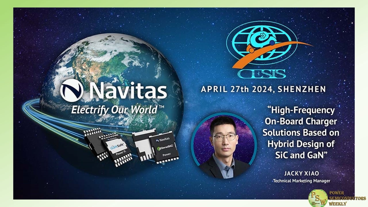
Navitas Semiconductor announced its participation in forthcoming China Electronic Hotspot Solutions Innovation Summit in Shenzhen on April 27th. The summit gathers key players in power semiconductors and associated customer design teams for innovations in EV such as 800 V supercharging, battery management, intelligent connected vehicle electronics, and high-power digital power supplies. 2024 EV OEM attendees include experts from Voyah and Dongfeng.
Jacky Xiao, Navitas’ Technical Marketing Manager, will deliver a keynote titled “High-Frequency On-Board Charger Solutions Based on Hybrid Design of SiC and GaN”, to introduce how Navitas can create more efficient, smaller and lighter on-board charging for EVs. Without compromise, customers can select Navitas’ optimal, feature-rich GaN and SiC power devices in robust, thermally-enhanced TOLL and TOLT packaging, to create hybrid powertrain solutions that deliver faster charging, longer range and lower systems costs.
Navitas’ GaNFast power ICs integrate GaN power and drive with control, sensing, and protection to enable faster charging, higher power density, greater energy savings and system cost reduction. New ‘Gen-3 Fast’ GeneSiC MOSFETs have up to 50% improved performance vs. other SiC devices. Summit exhibition attendees can explore the latest in EV-optimized GaNFast and GeneSiC products and complete EV system hardware solutions and learn how to accelerate their leading-edge projects.
“We’re delighted to participate in China Electronic Hotspot Solutions Innovation Summit, where we can discuss the technological trend of new energy industry with experts from renowned domestic institutions and leaders in international electronic components,” said Charles Zha, VP and GM of Navitas China. “Navitas’ leading GaN and SiC technology will enable faster charging, longer-range and more environmentally friendly power systems for EV. These improvements not only significantly enhance product performance but also effectively shorten time-to-market.”
The China Electronic Hotspot Solutions Innovation Summit will be held on April 27th, 2024, at Crowne Plaza, Nanshan District, Shenzhen.
Original – Navitas Semiconductor
-
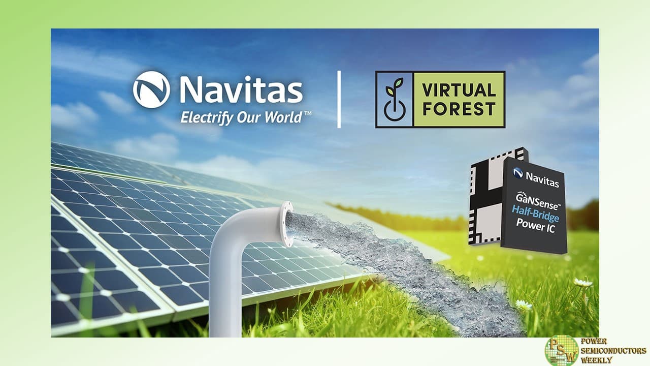
Navitas Semiconductor announced that Virtual Forest, one of India’s leading electronics design companies specializing in motor control and human interface technologies for consumer appliances, fluid movement and mobility, has adopted its GaNFast™ power integrated circuits (IC) technology for a zero-emission, powerful 3 hp (2,250W) solar-powered irrigation pump.
For many farmers worldwide, irrigating remote crops requires powerful pumps to lift water from rivers and streams up to field-level, with the majority powered by polluting and noisy diesel generators or expensive, lossy long-distance electrical cables. The Virtual Forest solar pump with maximum power point tracking (MPPT) operates in conjunction with solar panel and energy storage to provide robust, energy-independent and pollution-free performance at the point of use.
The 3 hp (2,250W) pump is remotely accessed via quad-band IoT with low power consumption. It can raise over 50 gallons-per-minute of water to a height of over 90 feet, enough to water 3 acres of farmland, and help to produce 10 tonnes of wheat. Further, the IoT enabled solar pump ensures optimal water usage through intelligent analytics, therefore minimizing ground water utilization.
Navitas GaNSense™ half-bridge power ICs monolithically by integrating two GaN power FETs with GaN drivers, level-shifters, protection features and high-efficiency loss-less current sensing. High-efficiency NV6269 half-bridge ICs, in easy-to-use 8×10 mm QFN packages are used in a 3-phase motor inverter, with 3x-5x energy savings vs legacy silicon IGBTs.
“The $450 million solar-pump market in India is expected to reach $1.5 Bn by 2026, calling for a solar revolution on Indian fields,” said Virtual Forest’s CEO, Omer Basith, adding “Reliable, off-grid systems are critical to overcome food insecurity and achieve energy efficiency. Leveraging Navitas’ high-power, efficient GaNSense™ half-bridge, we seek to deliver a robust solution to the market. We are nurturing our dream to drive gigatons of reduction in carbon emissions, thereby making the world a greener place to live in. Hence, our name — Virtual Forest.”
“The design team at Virtual Forest adopted the GaNSense half-bridges very quickly, for a fast time-to-market,” said Alessandro Squeri, Navitas’ Senior Sales Director. “With GaNSense, ‘easy-to-use feature, Virtual Forest comes into the partnership with high efficiency, low component count and a robust design for tough environments.”
Original – Navitas Semiconductor
-
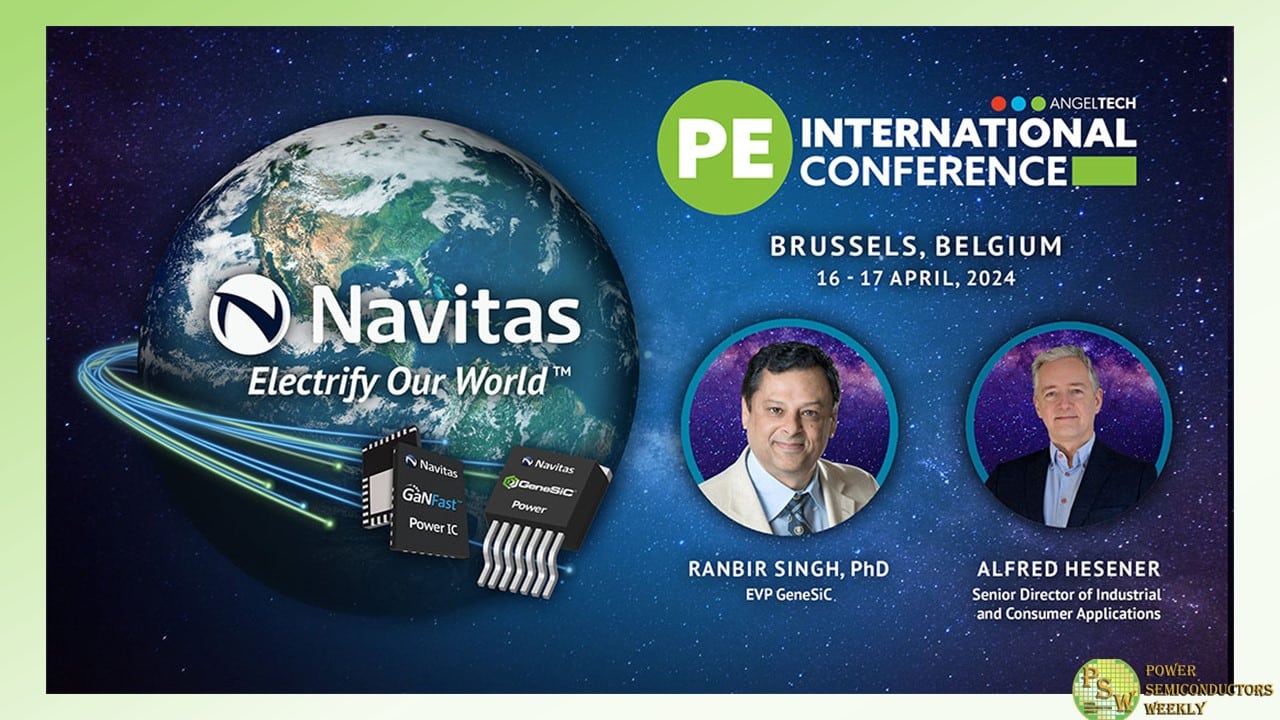
Navitas Semiconductor announced its participation in the upcoming Power Electronics International conference on April 16th– 17th 2024, in Brussels, Belgium.
Grid reliability is a key factor in a $1.3 trillion power semiconductor opportunity as Navitas’ technologies accelerate the transition from fossil fuels to renewable energies. Navitas will introduce the latest GaNFast™ and GeneSiC™ products to the European audience, including new Gen-3 Fast SiC for high-power and higher-speed performance, plus GaNSafe™ – the world’s most protected GaN power devices.
Navitas will present the following on April 17th:
- “3.3 kV SiC MOSFETs Accelerate Grid-Connected Energy Storage,” Dr. Ranbir Singh, EVP GeneSiC
Synopsis: The grid supplies energy from generators and delivers it to customers via transmission and distribution (T&D) networks. In the U.S., the use of electricity storage to support and optimize T&D has been limited due to high storage costs and limited design and operational experience. Recent improvements in storage and power technologies, however, coupled with changes in the marketplace, herald an era of expanding opportunity for electricity storage. SiC inverters will revolutionize electricity delivery, renewable energy integration, and energy storage. It is well-recognized that silicon-based semiconductors have inherent limitations that reduce their suitability for utility-scale applications.
- “Bi-directional circuits open up new opportunities in off-grid applications,” Alfred Hesener, Senior Director Industrial and Consumer Applications
Synopsis: Bi-directional circuits are critical to effectively smooth the supply/demand variation in renewable energy applications. In the past, they were expensive to make and complex to implement in power electronics applications. Wide bandgap GaN power ICs with integrated drive and advanced circuit functions deliver easy-to-use, reliable, high power density, and functionality for power factor correction circuits, solar inverters, and solid-state circuit breakers.
Original – Navitas Semiconductor
-
Navitas Semiconductor announced its participation in the forthcoming 2024 Asia Charging Expo (ACE) in Shenzhen, China, from March 20th to 22nd, 2024. Visitors will explore the latest advances in GaN and SiC toward a fully-electrified “Planet Navitas” and the transition from fossil fuels.
Navitas will introduce the latest GaNFast™ and GeneSiC™ products to the audience in China for the first time, including: GaNSense™ half-bridge power ICs with application-specific features and higher power ratings, Gen-3 Fast SiC power FETs for high-power and higher-speed performance, and the world’s most protected GaN power devices – GaNSafe™.
Teaming up with UGREEN, Navitas will showcase a variety of UGREEN fast chargers featuring GaNFast power ICs, including the adorable and popular 30W and 65W Nexode Robot chargers, 100W Nexode Magsafe Charger Stand, and high-power 300W Nexode 5-port Desktop Charging Station. Many more GaNFast™ chargers will be displayed for visitors to experience the lightning speed of GaNFast charging.
Ye Hu, Navitas’ Technical Marketing Manager, will deliver a keynote presentation titled “A New Chapter in GaN: Navitas’ Integrated Drive and Loss-less Current Sensing GaNSense™ Half-bridge Solution” as part of the exposition’s World GaN Conference on March 22nd.
ACE 2024 will be held at Hall 6, Futian Convention and Exhibition Center, Shenzhen, China from March 20th to 22nd. Visitors to “Planet Navitas” (booth B57-B60) will meet experienced Navitas engineers to explore the power of next-gen power semiconductors for leading-edge applications. Navitas sales and distribution partners will also provide on-site support.
“The Asia Charging Expo is a critical event in the power electronics industry – gathering key experts from mobile, EV and industrial companies – and we are delighted to be part of it again to present our latest GaN and SiC technology,” said Charles Zha, VP and GM of Navitas China. “Our latest, advanced GaNFast and GeneSiC technologies bring revolutionary fast-charging capabilities to industry-leading Chinese customers.”
Original – Navitas Semiconductor
