-

Toshiba Electronic Devices & Storage Corporation and Toshiba Corporation (Toshiba Group) have developed technology that mitigates the parasitic oscillation that occurs during switching operations by power modules with silicon carbide (SiC) MOSFETs connected in parallel, even with a 60% smaller gate resistance than is typical. The technology reduces power loss in power modules, mitigates oscillation, and realizes highly reliable switching operations.
The drive for carbon neutrality is stimulating demand for technologies that improve energy efficiency in many areas, including renewables, railways, and industrial equipment. In these sectors, the application of power modules built around SiC MOSFETs is seen as a solution that supports high-speed switching at high voltages and large currents—which is particularly important for the miniaturization of power converters, where higher switching frequencies result in higher rates of switching losses against power consumption.
Connecting multiple chips in parallel in power modules can form oscillation circuits, the result of wiring inductance between the chips and their parasitic capacitance. It can reduce module reliability if not countered, which is usually done by increasing gate resistance. However, this approach slows switching speed, resulting in a trade-off with switching losses. For power modules with SiC MOSFETs to perform high-speed switching, another approach is needed.
Toshiba Group used an equivalent circuit model of the power module (Figure 1) to determine the theoretical condition that triggers parasitic oscillation, and developed a wiring layout less likely to cause it. This was done by analyzing simulations of parasitic oscillation occurs when Lg/Ls, the ratio of gate-to-gate inductance Lg and source-to-source inductance Ls of parallel chips, is below a certain value (Figure 2). As increasing Lg/Ls is an effective means of mitigating parasitic oscillation, Toshiba Group fabricated prototype modules with different Lg/Ls and measured switching. This confirmed that increasing Lg/Ls mitigated oscillation, even with a 60% smaller gate resistance than that required by the alternative approach of increasing gate resistance (Figure 3).
Applying this approach to oscillation mitigation in power modules now under development has realized a power module less likely to cause parasitic oscillation, even with minimal gate resistance, that achieves low power loss with mitigated oscillation, and delivers highly reliable switching operation. Toshiba Group will continue to make refine the modules toward an early product launch.
Toshiba Group presented the details of this technology on June 6 at the 36th International Symposium on Power Semiconductor Devices and ICs (ISPSD) 2024, an international power semiconductor conference held in Bremen, Germany from June 2 to 6.
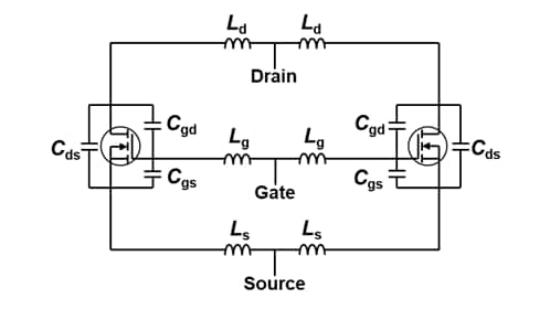
Figure 1. Model equivalent circuit of two MOSFETs connected in parallel 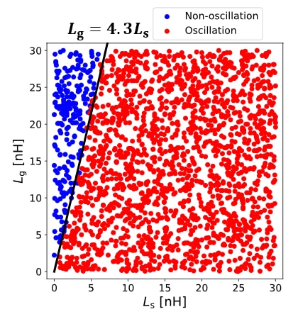
Figure 2. Simulation of oscillation in two MOSFETs with zero gate resistance connected in parallel 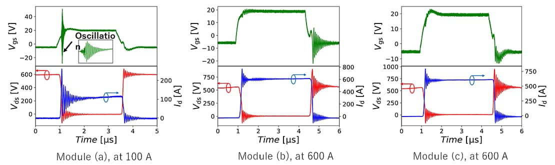
Vgs: Gate-Source voltage, Vds: Drain-Source voltage, Id: Drain current
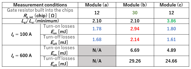
Figure 3. Switching waveforms and switching losses of the prototype modules (Source: Toshiba Group tests) Original – Toshiba
-

MCC introduced the latest additions to its robust portfolio: 10 1200V SiC N-channel MOSFETs in versatile TO-247-4, TO-247-4L, and TO-247AB packages. These new MOSFETs are available in 3-pin and 4-in (Kelvin source) configurations and meet the rising demand for high-power, high-voltage applications.
Boasting exceptional on-resistance values from 21mΩ to 120mΩ (typ.) and fast switching speeds, these components are the ones you can count on for reliable performance. Their excellent thermal properties and fast intrinsic body diode ensure smooth, efficient operation in the most challenging conditions, making them a must-have for critical power systems.
Features & Benefits:
- High-power capability: 1200V MOSFET with SiC technology
- Fast, reliable switching: Intrinsic body diode improves efficiency & ruggedness Enhanced performance: High switching speed with low gate charge
- Wide on-resistance selection: ranging from 21mΩ to 120mΩ (typ.)
- Efficiency: Superior thermal properties and low switching losses
- Durability: Avalanche ruggedness
- Versatility: TO247 3-pin and 4-pin package options
Original – Micro Commercial Components
-

Power Master Semiconductor has released 2nd generation of the 1200V eSiC MOSFET to meet the requirements of higher efficiency, high power density, robust reliability, and ruggedness in various applications such as DC EV charging stations, solar inverters, energy storage systems (ESS), motor drives and industrial power supplies. 1200V eSiC MOSFETs offer significant system advantages such as higher power density, efficiency and less cooling effort due to its much lower power losses.
Therefore, SiC MOSFETs are gaining popularity especially for renewable energy systems, EV charging systems that required higher power density, efficiency and robustness. DC EV charging station is level-3 charger and its power level is increasing by modular configuration as demand of faster charging time and higher battery capacity of EV. DC EV charging provides a mostly constant current output for wide DC output voltage range (200V to 900V) and load profile.
The new generation of 1200V eSiC MOSFET, Gen2 improved key FOM characteristics such as gate charge (QG), stored energy in output capacitance (EOSS), reverse recovery charger (QRR) and output charge (QOSS) by up to 30% compared to previous generation. This new generation SiC MOSFET technology offers significant system advantages such as smaller, lighter, higher efficiency, and less cooling effort thanks to its much lower power losses in various power conversion applications.
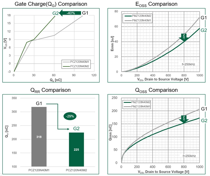
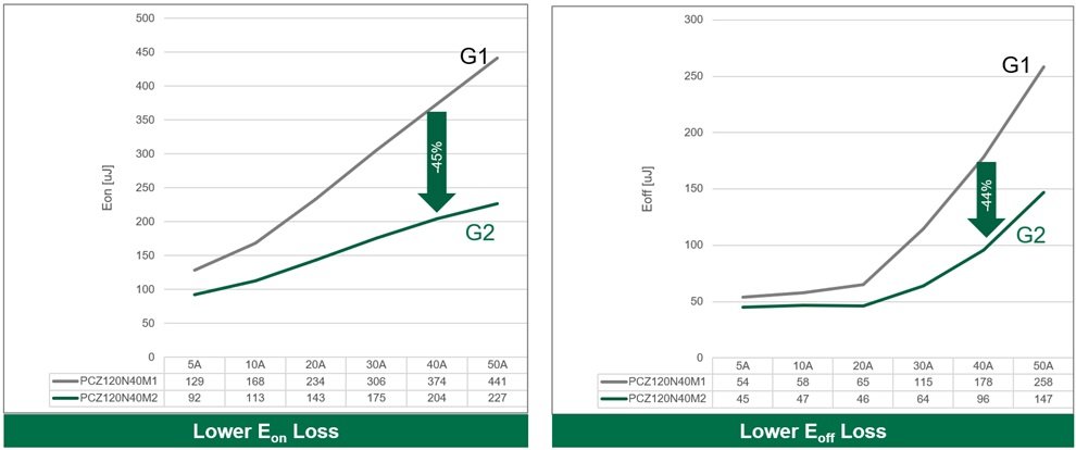
1200V eSiC MOSFET Gen2 offer excellent switching performance and 100% tested avalanche capability. It achieved 44% lower switching loss compared to the previous generation by extremely low miller capacitance (QGD).
Power Master Semiconductor is steadfastly committed to developing cutting-edge power device solutions that prioritize efficiency and sustainability,” said Namjin Kim, Sr. Director Sales & Marketing. “The introduction of our new generation of 1200V eSiC MOSFET marks a substantial leap forward in facilitating the development of cleaner, more efficient power systems. We are confident that the 1200V eSiC Gen2 MOSFET will play a transformative role in high-performance applications.
Original – Power Master Semiconductor
-

In the face of escalating climate crises and a dramatic rise in global energy demands, governments and industries are committing to ambitious climate goals aimed at mitigating environmental impact and securing a sustainable future. Key to these efforts is the transition to electrification to reduce carbon emissions and embrace renewable energy resources.
In a significant step towards accelerating this global transition, onsemi introduced its latest generation silicon carbide technology platform, EliteSiC M3e MOSFETs. The company also disclosed plans to release multiple additional generations through 2030.
“The future of electrification is dependent on advanced power semiconductors. Today’s infrastructure cannot keep up with the world’s demands for more intelligence and electrified mobility without significant innovations in power. This is critical to the ability to achieve global electrification and stop climate change,” said Simon Keeton, group president, Power Solutions Group, onsemi. “We are setting the pace for innovation, with plans to significantly increase power density in our silicon carbide technology roadmap through 2030 to be able to meet the growing demands for energy and enable the global transition to electrification.”
The EliteSiC M3e MOSFETs will play a fundamental role in enabling the performance and reliability of next-generation electrical systems at lower cost per kW, thus influencing the adoption and effectiveness of electrification initiatives. With the ability to operate at higher switching frequencies and voltages while minimizing power conversion losses, this platform is essential for a wide range of automotive and industrial applications such as electric vehicle powertrains, DC fast chargers, solar inverters and energy storage solutions.
Additionally, the EliteSiC M3e MOSFETs will enable the transition to more efficient, higher-power data centers to meet the exponentially increasing energy demands that power a sustainable artificial intelligence engine.
Through onsemi’s unique design engineering and manufacturing capabilities, the EliteSiC M3e MOSFETs achieve a significant reduction in both conduction and switching losses on the trusted and field-proven planar architecture. Compared to previous generations, the platform can reduce conduction losses by 30% and turn-off losses by up to 50%.
By extending the life of SiC planar MOSFETs and delivering industry-leading performance with EliteSiC M3e technology, onsemi can ensure the robustness and stability of the platform, making it a preferred choice for critical electrification applications
The EliteSiC M3e MOSFETs also offer the industry’s lowest specific on-resistance (RSP) with short circuit capability which is critical for the traction inverter market that dominates SiC volume. Packaged in onsemi’s state-of-the-art discrete and power modules, the 1200V M3e die delivers substantially more phase current than previous EliteSiC technology, resulting in approximately 20% more output power in the same traction inverter housing. Conversely, a fixed power level can now be designed with 20% less SiC content, saving costs while enabling the design of smaller, lighter and more reliable systems.
Additionally, onsemi provides a broader portfolio of intelligent power technologies including gate drivers, DC-DC converters, e-Fuses and more to pair with the EliteSiC M3e platform. The end-end onsemi combination of optimized, co-engineered power switches, drivers and controllers enable advanced features via integration, lowering overall system cost.
Global energy demands are projected to soar over the next decade, making the need for increased power density in semiconductors paramount. onsemi is leading innovation across its silicon carbide roadmap – from die architectures to novel packaging techniques – that will continue to address the general industry demand for increased power density.
With each new generation of silicon carbide, cell structures will be optimized to efficiently push more current through a smaller area, increasing power density. When coupled with the company’s advanced packaging techniques, onsemi will be able to maximize performance and reduce package size.
By applying the concepts of Moore’s Law to the development of silicon carbide, onsemi can develop multiple generations in parallel and accelerate its roadmap to bring several new EliteSiC products to market at an accelerated pace through 2030.
“We are applying our decades of experience in power semiconductors to push the boundaries of speed and innovation in our engineering and manufacturing capabilities to meet the rising global energy demands,” said Dr. Mrinal Das, senior director of technical marketing, Power Solutions Group, onsemi. “There is a huge technical interdependency between the materials, device and package in silicon carbide. Having full ownership over these key aspects allows us to have control over the design and manufacturing process and bring new generations to market much faster.”
The EliteSiC M3e MOSFET in the industry-standard TO-247-4L package is now sampling.
Original – onsemi
-

Toshiba Electronics Europe GmbH added two new 150V N-channel power MOSFET products based upon their latest generation U-MOS X-H Trench process. The TPH1100CQ5 and TPH1400CQ5 devices are designed specifically for use in high-performance switching power supplies, such as those used in data centres and communication base stations as well as other industrial applications.
With a maximum drain-source voltage (VDSS) rating of 150V and drain current (ID) handling 49A (TPH1100CQ5) and 32A (TPH1400CQ5), the new devices feature a maximum drain-source on-resistance RDS(ON).
The new products offer improved reverse recovery characteristics that are critical in synchronous rectification applications. In the case of TPH1400CQ5, the reverse recovery charge (Qrr) is reduced by approximately 73% to 27nC (typ.) and the reverse recovery time (trr) of 36 ns (typ.) is approximately 45% faster compared with Toshiba’s existing TPH1400CQH, which offers the same voltage and RDS(ON).
Used in synchronous rectification applications, the TPH1400CQ5 reduces the power loss of switching power supplies and helps improve efficiency. If the device is used in a circuit that does not operate in reverse recovery mode, the power loss is equivalent to that of the TPH1400CQH.
When used in a circuit that operates in reverse recovery mode, the new products reduce spike voltages generated during switching, helping to improve EMI characteristics of designs, and reducing the need for external filtering. The devices are housed in a versatile, surface-mount SOP Advance(N) package measuring just 4.9mm x 6.1mm x 1.0mm.
To support designers, Toshiba has developed a G0 SPICE model for rapid verification of the circuit function as well as highly accurate G2 SPICE models, for accurate reproduction of transient characteristics.
Shipments of the new devices start today, and Toshiba will continue to expand their lineup of power MOSFETs that help improve equipment efficiency.
Original – Toshiba
-

Toshiba Electronic Devices & Storage Corporation launched 650V N-channel power MOSFETs “TK068N65Z5, TK095E65Z5, TK095A65Z5, TK095V65Z5, TK115E65Z5, TK115A65Z5, TK115V65Z5 and TK115N65Z5” and added them to the lineup of Toshiba’s latest-generation DTMOSVI series with high-speed diodes (DTMOSVI (HSD)) that uses super junction structure and is suitable for high-efficiency switching power supplies for data centers and power conditioners for photovoltaic generators. Packages of the new products are TO-247, TO-220SIS, TO-220 and DFN8×8.
The new products with the DTMOSVI (HSD) process use high-speed diodes to improve the reverse recovery characteristics important for bridge circuit and inverter circuit applications. Against Toshiba’s existing product TK090A65Z of the standard type DTMOSVI, the new product TK095A65Z5 achieves an approximately 65% reduction in reverse recovery time (trr), and an approximately 88% reduction in reverse recovery charge (Qrr) (measurement conditions: -dIDR/dt=100A/μs).
In addition, the DTMOSVI (HSD) process improves on the reverse recovery characteristics of Toshiba’s existing products DTMOSIV series with high-speed diodes (DTMOSIV (HSD)), and has a lower drain cut-off current at high temperatures. Furthermore, the figure of merit “drain-source On-resistance × gate-drain charge” is also lower.
The high temperature drain cut-off current of the new product TK095A65Z5 is approximately 91% lower, and the drain-source On-resistance × gate-drain charge approximately 70% lower, than in Toshiba’s existing product TK35A65W5. This advance will cut equipment power loss and help to improve efficiency.
A reference design, “1.6kW Server Power Supply (Upgraded)“, that uses the same series product TK095N65Z5 is available on Toshiba’s website.
Toshiba also offers tools that support circuit design for switching power supplies. Alongside the G0 SPICE model, which verifies circuit function in a short time, highly accurate G2 SPICE models that accurately reproduce transient characteristics are now available.
Toshiba also will continue to expand its lineup of the DTMOSVI series. This will enhance switching power supply efficiency, contributing to energy-saving equipment.
Applications
Industrial equipment
- Switching power supplies (data center servers, communications equipment, etc.)
- EV charging stations
- Power conditioners for photovoltaic generators
- Uninterruptible power systems
Features
- MOSFETs with high-speed diodes in the latest-generation DTMOSVI series
- Reverse recovery time due to high-speed diodes:
TK068N65Z5 trr=135ns (typ.)
TK095E65Z5, TK095A65Z5, TK095V65Z5 trr=115ns (typ.)
TK115E65Z5, TK115A65Z5, TK115V65Z5, TK115N65Z5 trr=110ns (typ.) - High-speed switching time due to low gate-drain charge:
TK068N65Z5 Qgd=22nC (typ.)
TK095E65Z5, TK095A65Z5, TK095V65Z5 Qgd=17nC (typ.)
TK115E65Z5, TK115A65Z5, TK115V65Z5, TK115N65Z5 Qgd=14nC (typ.)
Original – Toshiba
-
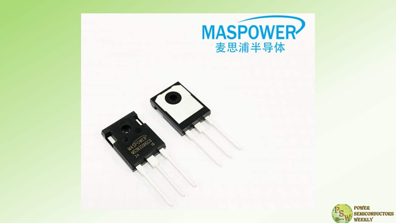
In the current rapidly evolving electronics industry, there is an increasing demand for high-performance MOSFETs. With its superior specifications and robust design, the MS2N350HGC0 MOSFET stands out as an innovative solution for a wide range of high-voltage applications.
The MS2N350HGC0 MOSFET has been designed to meet the rigorous specifications of contemporary electronics, offering an unparalleled combination of features and performance. This MOSFET is the ideal choice for high-voltage power supplies, capacitor discharge, pulse circuits and laser and X-ray generation systems. With a maximum drain-source voltage of 3500V and a continuous drain current of 2A, it is capable of withstanding the high voltage applications on the market.
One of the standout features of the MS2N350HGC0 is its rapid intrinsic diode and minimized gate charge.. This enables the device to operate at high speeds, which is crucial for applications that necessitate rapid response times. Moreover, the MOSFET exhibits exceedingly low intrinsic capacitances, which further enhances its performance in demanding applications.
The MS2N350HGC0’s on-state resistance (Rds) of 19Ω further enhances its performance, allowing for efficient energy transfer and minimal heat generation. This makes it an excellent choice for power supplies and other applications where efficiency and reliability are paramount.
The product is packaged in accordance with the industry standard TO-247, thereby ensuring compatibility with a wide range of existing systems. Its compact size and lightweight design facilitate integration into any application.
The MOSFET’s electrical ratings are noteworthy for their impressive nature. This product is capable of withstanding a continuous drain current of 2A at 25°C and 1.6A at 100°C, with a pulsed drain current of up to 6A. This makes it suitable for even the most demanding applications. Furthermore, its total dissipation of 463 watts at 25°C guarantees reliable operation even under heavy load conditions.
The MS2N350HGC0 also offers excellent avalanche and thermal performance. It has an avalanche current of 1.3A and can withstand a single pulse avalanche energy of 81mJ. The operating junction temperature ranges from -55°C to 150°C, ensuring stable performance even in extreme environments.
For ease of installation, the MS2N350HGC0 has a maximum lead temperature for soldering purposes of 300°C and a mounting torque of 1.13N·m. This ensures that the MOSFET can be securely mounted into any system with minimal effort.
In conclusion, the MS2N350HGC0 MOSFET is a powerful and reliable solution for high-voltage applications. The superior performance, compact design, and excellent thermal stability of the product make it the optimal choice for a diverse range of applications. To gain further insight into this innovative new product, we invite you to contact our sales team. We encourage you to explore the potential of the MS2N350HGC0 MOSFET and discover how it can revolutionize your high-voltage applications.
Original – Maspower Semiconductor
-
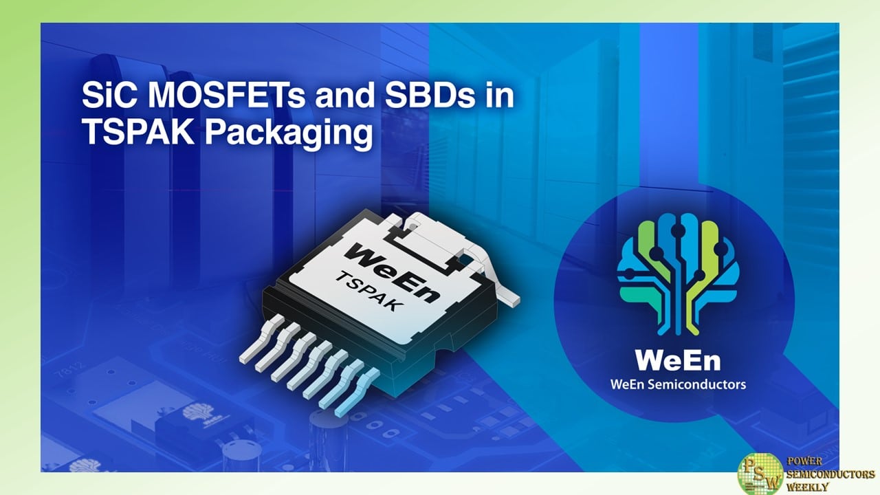
WeEn Semiconductors unveiled new families of silicon carbide (SiC) MOSFETs and Schottky Barrier Diodes (SBDs) in TSPAK packaging at this year’s PCIM Europe exhibition and conference. The company has also used the event to showcase for the first time a comprehensive range of integrated SiC power modules in Nuremberg, from June 11-13, 2024.
WeEn Semiconductor’s new TSPAK MOSFET and SBD devices address the demand for high-performance, compact and reliable power management in applications ranging from automotive charging and on-board charger applications to photovoltaic (PV) inverters and high-power-density power supplies (PSUs).
Offering a variety of configuration options for maximum design flexibility, the company’s new SiC modules are ideal for applications such as EV charging, energy storage systems, PV inverters, motor drives, industrial PSUs and test instrumentation.
Originally developed for automotive applications, TSPAK devices combine innovative top-side cooling capability with low thermal impedance to deliver enhanced thermal performance. By removing the PCB thermal resistance from the thermal dissipating path, the Junction-Ambient thermal resistance improves by 16-19%.
This supports high reliability by enabling a greater number of power cycles than conventional packaging as well as providing the increased power densities demanded by compact system designs. Low circuit inductance and low EMC noise help to improve performance and reduce filtering requirements. The WeEn Semiconductors family of TSPAK MOSFETs features 650V, 750V, and 1200V options with resistances ranging from 12mΩ to 150mΩ. TSPAK SBDs are available with current ratings of 10 to 40A in 650V, 750V, and 1200V variants.
Visitors to WeEn’s stand in Hall 9, booth 538, will have the first opportunity to explore the company’s extensive range of SiC power modules. With a wide range of topology options, including half-bridge, four-pack, six-pack, and MPPT booster configurations, the power modules support voltages ranging from 650V to 1200V. Depending on the option chosen and special designs, modules incorporate a variety of advanced features including synchronized chip current sharing, integrated temperature sensors, topside cooling structures and the latest clip-bond technologies.
Original – WeEn Semiconductors
-
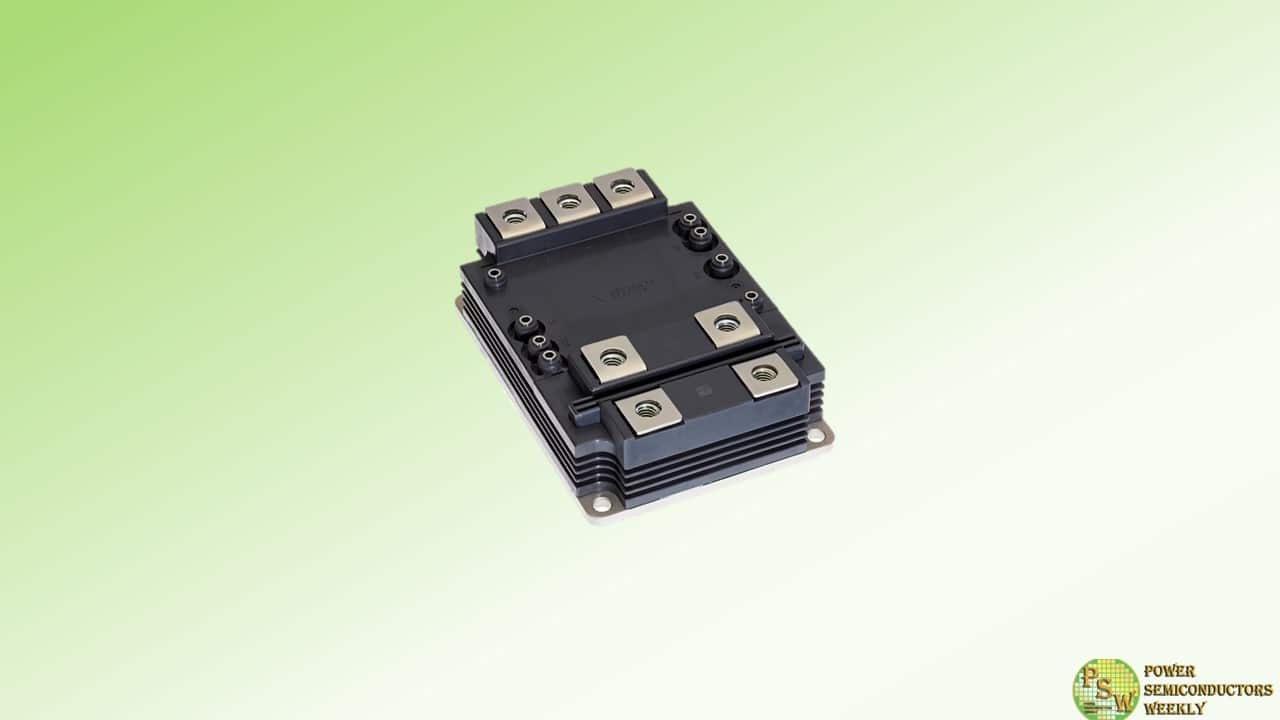
Mitsubishi Electric Corporation has begun shipping low-current 3.3kV/400A and 3.3kV/200A versions of a Schottky barrier diode (SBD) embedded silicon carbide (SiC) metal-oxide-semiconductor field-effect transistor (MOSFET) module for large industrial equipment, including rolling stock and electric power systems, from today, June 10.
Together with the existing 3.3kV/800A version, the newly named UnifullTM series comprises three modules to meet the growing demand for inverters capable of increasing power output and power conversion efficiency in large industrial equipment. The new modules will be exhibited at major trade shows, including Power Conversion Intelligent Motion (PCIM) Europe 2024 in Nuremberg, Germany from June 11 to 13.
Mitsubishi Electric’s SBD-embedded SiC-MOSFET modules, including the 3.3kV/800A version released on March 29, feature an optimized package structure to reduce switching loss and improve SiC performance. Compared to existing power modules, UnifullTM modules, significantly reduce switching loss and contribute to higher power output and efficiency in large industrial equipment, making them suitable for auxiliary power supplies in railcars and drive systems with relatively small capacities.
Original – Mitsubishi Electric
-

Vishay Intertechnology, Inc. announced that at PCIM Europe 2024 the company will be showcasing its broad portfolio of power management solutions that address several increasingly important trends in power electronics, including e-mobility, high efficiency power conversion, energy storage, and grid management. In Hall 9, Booth 208, Vishay experts will be available to discuss the company’s extensive offering of passive and semiconductor solutions for these next-generation applications.
Taking center stage for Vishay at PCIM will be the company’s newly released 1200 V MaxSiC™ series silicon carbide (SiC) MOSFETs, which deliver on-resistances of 55 mW, 95 mW, and 280 mΩ in standard packages for industrial applications, with custom products also available.
In addition, Vishay will provide a roadmap for 650 V to 1700 V SiC MOSFETs with on-resistances ranging from 10 mΩ to 1 Ω. Vishay’s SiC platform is based on proprietary MOSFET technology — enabled through the company’s acquisition of MaxPower Semiconductor, Inc. — which will address market demands in traction inverter, photovoltaic energy conversion and storage, on-board charger, and charging station applications. At the booth, Vishay’s experts will also be discussing upcoming planned releases of the MaxSiC platform, including AEC-Q101 Automotive Grade products.
At PCIM, Vishay will be offering a variety of application-focused demonstrations, including:
- A high voltage intelligent battery shunt for 400 V and 800 V batteries
- A 40 kW resettable electronic fuse (eFuse) for 400 V and 800 V battery electric vehicles (BEV)
- A unidirectional, 11 kW three-phase AC on-board charger (OBC) with a BOM consisting of 90 % Vishay parts
- A bidirectional 10 kW eFuse for 48 V applicationsA collaborative robot workstation featuring Vishay power resistors, ESTA power electronic capacitors (PEC), Automotive Grade diodes, SiC MOSFETs, and an SiC-based auxiliary power converter.
Vishay passive components on display at PCIM will include IHPT series solenoid-based haptic actuators featuring Immersion Corporation licenses, a 5.5 kW transformer / inductor for LLC applications, and IHLE® series low profile, high current inductors with integrated e-field shields; wirewound resistors and charging resistors featuring hybrid wirewound technology; thick film power resistors; robust metallized polypropylene film capacitors, including AC and pulse capacitors and DC-Link capacitors with high temperature operation up to +125 °C and the ability to withstand temperature humidity bias (THB) testing of 85 °C / 85 % for 1000 h; X1, X2, and Y2 EMI suppression film capacitors certified to safety and humidity robustness grade IIIB; and DC and AC power electronic capacitors (PEC) with high impulse current ratings, low inductance, and high reliability.
Highlighted Vishay semiconductor solutions will consist of surface-mount diodes in the eSMP® and FlatPAK 5×6 packages; leadless surface-mount diodes in the DFN, CLP, and LLP series packages; and 650 V and 1200 V SiC Schottky diodes up to 20 A in eSMP® series and 40 A in power packages for AC/DC power factor correction (PFC) and ultra high frequency output rectification. In addition, Vishay will be showcasing microBUCK® and microBRICK® buck regulators, including the 60 V input SiC967 synchronous buck regulator with integrated power MOSFETs and inductors; high voltage MOSFETs in the PowerPAK 10×12 package; automotive power modules in the EMIPAK 1B, MaacPAK, FlatPAK, and HC0 packages; and industrial power modules in Gen III TO-244, IAP, SOT-227, and MTC packages.
Prior to the exhibition, on June 9, Vishay’s Sanjay Havanur — senior manager of system applications — will be presenting the seminar “Silicon Is Still Here: A Refresher on the Narrow Bandgap Power MOSFETs and Their Datasheets” at 2 p.m. in the Arvena Park Hotel. During the show, Claudio Damilano — director of product marketing and market development, power modules — will present “Evolution in Vishay Power Modules for E-Mobility: Solutions for High Voltage and Low Voltage Applications” on June 11, at 3:50 p.m. in Hall 6, Booth 220.
Original – Vishay Intertechnology
