-

Many industrial applications today are moving towards higher power levels with minimized power losses. One way to achieve this is to increase the DC link voltage. Infineon Technologies AG is addressing this market trend with the CoolSiC™ Schottky diode 2000 V G5 product family, the first discrete silicon carbide diodes with a breakdown voltage of 2000 V, introduced in September 2024.
The product portfolio has now been expanded to include a Schottky diode in the TO-247-2 package, which is pin-compatible with most existing TO-247-2 packages. The product family fits perfectly for applications with DC link voltages up to 1500 V DC, making it ideal for solar and EV chargers.
The CoolSiC Schottky diode 2000 V G5 in the TO-247-2 package is available with current ratings ranging from 10 to 80 A. It allows developers to achieve higher power levels in their applications while reducing the component count by half compared to 1200 V solutions. This simplifies the overall design and facilitates a seamless transition from multi-level to two-level topologies.
In addition, the Schottky diode in the TO-247-2 package incorporates .XT interconnection technology, which significantly reduces thermal resistance and impedance, thereby enhancing heat management. Humidity robustness has been validated through HV-H3TRB reliability testing. The diodes exhibit neither reverse recovery nor forward recovery, and feature a low forward voltage, ensuring improved system performance.
The 2000 V diode family is a perfect match for the CoolSiC MOSFETs 2000 V in the TO-247Plus-4 HCC package that Infineon launched in the spring of 2024. In addition to the TO-247-2 package, the CoolSiC Schottky Diode 2000 V is also available in the TO-247PLUS-4 HCC package.
Original – Infineon Technologies
-

Infineon Technologies AG has introduced its roadmap for next-level Battery Backup Unit (BBU) solutions for uninterrupted operations of AI data centers to avoid power outages and the risk of data losses. The comprehensive BBU roadmap includes power solutions from 4 kW up to the world’s first 12 kW battery backup unit. The BBU solutions are designed to deliver highly efficient, reliable, and scalable power conversion in AI server racks, and achieve a power density up to 400 percent higher compared to industry average.
BBUs are essential for AI data centers to provide an uninterruptible power supply and furthermore protect sensitive AI hardware from voltage spikes, surges, and other power anomalies by filtering and conditioning the power that is supplied to the data center equipment. Combined with various best-in-class topologies enabling an increased ease-of-use for customers, the BBU solutions are bolstering Infineon’s leading position in the field of powering artificial intelligence.
“Ensuring an uninterrupted power supply to AI systems is critical for maintaining process continuity and seamless operation,” said Adam White, Division President Power & Sensor Systems at Infineon. “Our energy efficient battery backup units are designed to keep AI servers running smoothly with exceptional performance, flexibility, and efficiency catering to the diverse power levels required by AI servers. By mastering all three relevant semiconductor materials silicon (Si), silicon carbide (SiC), and gallium nitride (GaN) we are confident that Infineon semiconductor solutions will set a new standard in powering AI data centers.”
Downtime or system failures in AI data centers can be extraordinarily costly, with 41 percent of firms interviewed in an ITIC survey from 2024 indicating losses from $1 million to over $5 million per hour of downtime. 35 percent of these failures are attributed to issues with power component quality. To address this, Infineon’s Partial Power Converter (PPC), a semiconductor solution that focuses on improving performance and reliability of power supply systems, stands out as a leading technology for battery backup units.
The intermediate solution, represented by the 5.5 kW BBU, features an Infineon proprietary topology that integrates Si and GaN technologies providing ultra-high efficiency and high-power density. The industry-first 12 kW system combines several 4 kW power converter cards utilizing Infineon’s PSOC™ microcontrollers, 40 V and 80 V OptiMOS™ and EiceDRIVER™ Gate Drivers enabling unparalleled performance and flexibility, achieving a power density four times higher than industry average.
Higher power levels can be attained by paralleling multiple cards on a motherboard, offering ease of scalability and simplified maintenance. If one card fails, the system continues to operate at a reduced capacity, minimizing downtime and ensuring high reliability. This modular approach allows the system to be tailored to specific power requirements without the need for a full system redesign creating substantial customer benefits in performance and reliability.
To further demonstrate the capabilities of the latest BBU technology, Infineon is developing full system demonstrators for its battery backup solutions. These demonstrators will showcase the advantages of the PPC technology in real-world applications offering a clear path forward for next-generation AI data centers.
Original – Infineon Technologies
-

Infineon Technologies AG launched the next generation of high-density power modules which play a pivotal role in enabling AI and high-performance compute. Through enhanced system performance and with Infineon’s trademark robustness, the new OptiMOS™ TDM2454xx quad-phase power modules enable best-in-class power density and total-cost-of-ownership (TCO) for AI data centers operators.
The OptiMOS TDM2454xx quad-phase power modules enable true vertical power delivery (VPD) and offer industry’s best current density of 2 Ampere per mm². The modules follow the OptiMOS TDM2254xD and the OptiMOS TDM2354xD dual-phase power modules introduced by Infineon last year, and continue to enable superior power density for accelerated compute platforms.
In traditional horizontal power delivery systems, power needs to travel across the surface of the semiconductor wafer, which can result in higher resistance and significant power loss. Vertical power delivery minimizes the distance that power needs to travel, thereby reducing resistive losses enabling increased system performance.
Data centers are currently responsible for two percent of global energy consumption according to the IEA. Fueled by AI, the power demands within data centers are expected to grow by 165% between 2023 and 2030. Continually improving the efficiency and power densities of power conversion from grid-to-core is vital to enable further advancements in compute performance while reducing TCO.
“We are proud to expand our high-performance AI data center solutions with the OptiMOS TDM2454xx VPD modules,” said Rakesh Renganathan, Vice President Power ICs at Infineon Technologies. “We take a three-dimensional design approach and leverage our industry-leading power devices, packaging technologies and extensive systems expertise to provide high-performance and energy-efficient computing solutions as part of our mission to drive digitalization and decarbonization.”
The OptiMOS TDM2454xx modules are a fusion of Infineon’s robust OptiMOS 6 trench technology, chip-embedded package for superior electrical and thermal efficiencies, and innovative low-profile magnetic design that continue to push the envelope for performance and quality of VPD systems.
Additionally, the OptiMOS TDM2454xx has a footprint that is designed to enable module tiling and improving current flow that enhance electrical, thermal and mechanical performance. The OptiMOS TDM2454xx modules support up to 280A across four phases with an integrated embedded capacitor layer within a small 10x9mm² form factor. Combined with Infineon’s XDP™ controllers, they offer a robust power solution with improved system power density.
The OptiMOS TDM2454xx modules are further strengthening Infineon’s unique position in the market with the broadest product and technology portfolio based on all relevant semiconductor materials to power different AI server configurations from grid to core in the most energy efficient way.
Original – Infineon Technologies
-
Infineon Technologies AG announced the addition of P-channel power MOSFETs to its family of radiation-tolerant power MOSFETs for Low-Earth-Orbit (LEO) space applications. The new devices are part of Infineon’s expanding portfolio designed for next-generation “NewSpace” applications, providing cost-optimized radiation-tolerant MOSFETs that enable engineers to achieve faster time-to-market designs using smaller and lighter weight components with radiation performance suitable for missions lasting two to five years.
“Successful deployment of next-generation LEO satellite constellations and other space-ready systems require radiation-tolerant discretes and ICs with lead times and production volumes that enable rapid deployment and cost optimization,” said Chris Opoczynski, Sr. VP and General Manager, High Reliability (HiRel) Business, Power and Sensor Systems Division, Infineon . “Infineon is leveraging its 50-years of space heritage to bring an industry-first portfolio of efficient and reliable power devices to this dynamic sector of the business.”
The new 60 V P-channel MOSFET complements the already available 60 V and 150 V N-channel devices, all offered in plastic packaging, which is lower in cost than the traditional hermetic packaging used in rad-hardened devices and can be produced in higher volumes using standard manufacturing practices.
The radiation-tolerant discretes are qualified for space applications according to the relevant tests of the AEC-Q101 standard. Additional package tests such as outgas and salt atmosphere tests are included as part of the qualification, and they are rated for Single Event Effects (SEE) at 46 MeV∙cm²/mg LET and a Total Ionizing Dose (TID) of 30 to 50 krad (Si). The operating temperature rating is -55 °C to 175 °C (maximum). State-of-the-art technologies, like the patented CoolMOS™ superjunction technology used for the N-channel MOSFETs enables Field Effect Transistors (FETs) from Infineon to offer fast switching capabilities as compared to alternative solutions.
Original – Infineon Technologies
-

SkyWater Technology has entered into an agreement with Infineon Technologies AG for SkyWater to purchase Infineon’s 200 mm fab in Austin, Texas, (“Fab 25”) and a corresponding long-term supply agreement. SkyWater will operate the fab as a foundry, increasing available capacity in the U.S. for foundational chips on nodes from 130 nanometers down to 65 nanometers that are critical for many industrial, automotive and defense applications.
Fab 25 will also substantially increase SkyWater’s scale as a foundry and provide additional capabilities such as 65 nm infrastructure, expanded copper processing scale and high-voltage Bipolar-CMOS-DMOS (BCD) technology. The long-term supply agreement will enable Infineon to maintain a strong, efficient and scalable manufacturing footprint in the United States.
Infineon and SkyWater believe that this strategic partnership will enhance the long-term viability and utilization of Fab 25. The transaction also affirms the long-term perspective for nearly 1,000 manufacturing jobs at Fab 25, since all current Fab 25 employees will become SkyWater employees as part of the agreement.
SkyWater is a U.S.-based company with access to a broad customer base and a Trusted supplier of the U.S. Department of Defense. SkyWater believes the transaction will allow it to realize significant economies of scale, bring high-value manufacturing services to SkyWater’s customers and support dual sourcing strategies for critical industries.
Furthermore, SkyWater plans to transition the Fab 25 business model from Integrated Device Manufacturer (IDM) to foundry to bring substantial manufacturing capacity to a broad base of new customers over time. Foundational semiconductors are of strategic importance for several U.S. industries, including the defense sector. The partnership will strengthen the industrial base and domestic semiconductor supply chain in the U.S. as well as the resilience for critical foundational semiconductor technology. The closing of the transaction is subject to regulatory approval in the U.S. and is expected in the coming months.
“The transaction fully aligns with Infineon’s manufacturing strategy to create synergies with strategic foundry partners when in-house manufacturing does not offer competitive advantages,” said Alexander Gorski, Executive Vice President and Head of Frontend Operations at Infineon. “The partnership with SkyWater creates mutual benefits and synergies, supports our profitable growth and provides us with a strong and trusted foundry partner, thereby safeguarding our long-term supply base in the U.S. We commend the contributions the Fab25 team has made to our operations and thank the Austin community and our local and federal partners for their support and collaboration.”
“This milestone expands our partnership with Infineon and significantly increases our U.S. foundry capacity. We expect it will also enhance supply chain resilience for foundational chips that are critical to sensitive, strategic applications, thereby strengthening both national and economic security,” said Thomas Sonderman, SkyWater CEO. “This investment is an expansion that enhances our ability to serve both our defense and industrial customers. By leveraging the proven expertise of the talented team in Austin, we are positioning this fab as a cornerstone in the U.S. semiconductor foundry network—one that will extend our capabilities to support defense programs while also enabling new opportunities in commercial markets. ”
The U.S. is a key business region for Infineon with around 4,000 employees, 15 locations dedicated to research and development activities and 1,000 employees in R&D roles. Infineon serves a multitude of American customers across all its market segments in automotive, industrial & infrastructure, as well as consumer, computing & communications. Currently, up to one billion semiconductor chips per year for major automotive, industrial and communications companies are manufactured in Fab25.
Original – Infineon Technologies
-

Manufacturers of cutting-edge audio equipment constantly seek to enhance sound quality while also meeting the growing demand for compact, lightweight, more integrated, and energy-efficient designs. At the same time, they must ensure seamless connectivity, cost-effectiveness, and user-friendly functionality, making audio product development more complex than ever.
To overcome these challenges, SounDigital has integrated CoolGaN™ transistors from Infineon Technologies AG into its new 1500 W Class D amplifier, featuring an 800 kHz switching frequency and five channels. Infineon’s advanced GaN technology has improved the energy efficiency of the amplifier by five percent and reduced energy loss by 60 percent.
“We are excited to enhance the performance of our audio amplifiers using Infineon’s GaN power semiconductors, enabling us to inspire people and provide entertainment by amplifying music around the world,” said Juliano Anflor, CEO of SounDigital. “GaN transistors significantly enhances our overall system performance with minimized system cost and increased ease of use.”
“GaN technology is transforming the audio amplifier industry, providing unparalleled efficiency and performance,” said Johannes Schoiswohl, Head of the GaN Business Line at Infineon. “Infineon’s leading GaN solutions deliver superior sound quality, higher power density, and reduced energy consumption, enabling SounDigital’s audio systems to reach new levels of fidelity and performance.”
For its 1500 W Class D amplifier, SounDigital selected Infineon’s 100 V normally-off E-mode transistors: IGC033S101 in a PQFN-3×5 package and IGB110S101 in a PQFN-3×3 package. With their low on-resistance, the transistors are ideal for demanding high-current applications, enabling significant improvements in both sound quality and efficiency of SounDigital’s amplifier.
The GaN-based amplifier also delivers high performance while reducing power dissipation by 75 W, allowing for a 50 percent smaller heat sink. Additionally, the overall system size has been reduced by 40 percent without compromising performance. The audio quality has been further improved by the CoolGaN transistors, with total harmonic distortion (THD) reduced by 70 percent, enabling a more precise and detailed sound experience. At the same time, the idle current has been reduced by 40 percent, significantly improving energy efficiency.
Original – Infineon Technologies
-

The European Commission approved funding under the European Chips Act for the Infineon Technologies AG Smart Power Fab in Dresden. The official funding approval from the Federal Ministry for Economic Affairs and Climate Action (BMWK), which is responsible for the disbursement of EU Chips Act funding, is still pending and is expected within the next few months.
Additionally, the Smart Power Fab is already receiving support under the European Commission’s IPCEI ME/CT (“Important Project of Common European Interest on Microelectronics and Communication Technologies”) innovation program. The total funding for the Dresden site amounts to around one billion euros. Construction began in March 2023 and is progressing successfully. The Fab opening is planned for 2026.
“This government-supported investment by Infineon strengthens the position of Dresden, Germany and Europe as a semiconductor hub and promotes a state-of-the-art innovation and production ecosystem for microelectronics,” says Jochen Hanebeck, CEO of Infineon. “We are increasing semiconductor capacity in Europe and thus helping secure stable supply chains in automotive, security and industrial fields.”
Infineon is investing a total of five billion euros in the expansion of its Dresden site. The German federal government previously approved the early start of the project. The new development will create up to 1,000 new jobs, not including the additional jobs created in the ecosystem of the investment. Experts assume a positive job effect of 1:6. The core of the Smart Power Fab will focus on technologies that further accelerate decarbonization and digitalization for example by driving energy-efficient power solutions for Artificial Intelligence.
In addition to the funding for the expansion of manufacturing in Dresden, Infineon is also leveraging the IPCEI ME/CT innovation program to drive investments in research and development at other corporate locations. Between 2022 and 2027 Infineon will have invested 2.3 billion euros in innovation projects at its sites in Germany and Austria, concentrated in the fields of power electronics, analog/mixed-signal technologies, sensor technologies and radio frequency applications.
As part of the EU funding programs, Infineon is furthermore planning comprehensive measures to promote partnership between science and industry. A central element is close collaboration with European universities, research institutions and start-ups. Infineon offers talented young individuals a platform for developing and advancing sustainable innovations. These activities promote the hands-on application of scientific knowledge and strengthen Europe’s position as an innovation hub.
Original – Infineon Technologies
-
Gallium Nitride (GaN) technology plays a crucial role in enabling power electronics to reach the highest levels of performance. However, GaN suppliers have thus far taken different approaches to package types and sizes, leading to fragmentation and lack of multiple footprint-compatible sources for customers.
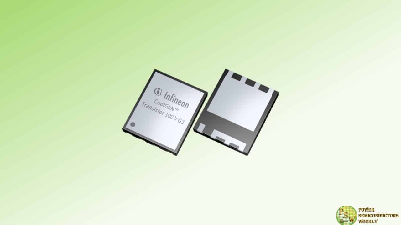
Infineon Technologies AG addresses this challenge by announcing the high-performance gallium nitride CoolGaN™ G3 Transistor 100 V in RQFN 5×6 package (IGD015S10S1) and 80 V in RQFN 3.3×3.3 package (IGE033S08S1).
“The new devices are compatible with industry-standard silicon MOSFET packages, meeting customer demands for a standardized footprint, easier handling and faster-time-to-market,” said, Dr. Antoine Jalabert, Product Line Head for mid-voltage GaN at Infineon.
The CoolGaN G3 100 V Transistor devices will be available in a 5×6 RQFN package with a typical on-resistance of 1.1 mΩ. Additionally, the 80 V transistor in a 3.3×3.3 RQFN package has a typical resistance of 2.3 mΩ. These transistors offer a footprint that, for the first time, allows for easy multi-sourcing strategies and complementary layouts to Silicon-based designs. The new packages in combination with GaN offer a low-resistance connection and low parasitics, enabling high performance transistor output in a familiar footprint.
Moreover, this chip and package combination allows for high level of robustness in terms of thermal cycling, in addition to improved thermal conductivity, as heat is better distributed and dissipated due to the larger exposed surface area and higher copper density.
Samples of the GaN transistors IGE033S08S1 and IGD015S10S1 in RQFN packages will be available in April 2025.
Original – Infineon Technologies
-

Infineon Technologies AG has made significant progress on its 200 mm silicon carbide (SiC) roadmap. The company will already release the first products based on the advanced 200 mm SiC technology to customers in Q1 2025. The products, manufactured in Villach, Austria, provide first-class SiC power technology for high-voltage applications, including renewable energies, trains, and electric vehicles. Additionally, the transition of Infineon’s manufacturing site in Kulim, Malaysia, from 150-millimeter wafers to the larger and more efficient 200-millimeter diameter wafers is fully on track. The newly built Module 3 is poised to commence high-volume production aligned with market demand.
“The implementation of our SiC production is progressing as planned and we are proud of the first product releases to customers,” said Dr. Rutger Wijburg, Chief Operations Officer of Infineon. “By ramping up SiC production in Villach and Kulim in phases, we are improving cost-efficiency and continuing to ensure product quality. At the same time, we are making sure our manufacturing capacities can meet the demand for SiC-based power semiconductors.”
SiC semiconductors have revolutionized high-power applications by switching electricity even more efficiently, demonstrating high reliability and robustness under extreme conditions, and by making even smaller designs possible. Infineon’s SiC products let customers develop energy-efficient solutions for electric vehicles, fast charging stations and trains as well as renewable energy systems and AI data centers.
The release to customers of the first SiC products based on the 200-millimeter wafer technology marks a substantial step forward in Infineon’s SiC roadmap, with a strong focus on providing customers with a comprehensive portfolio of high-performance power semiconductors that promote green energy and contribute to CO 2 reduction.
As “Infineon One Virtual Fab” for highly innovative wide-bandgap (WBG) technologies, Infineon’s production sites in Villach and Kulim share technologies and processes which allow for fast ramping and smooth and highly efficient operations in SiC and gallium nitride (GaN) manufacturing. The 200-millimeter SiC manufacturing activities now add to Infineon’s strong track record of delivering industry-leading semiconductor technology and power system solutions and strengthen the company’s technology leadership across the entire spectrum of power semiconductors, in silicon as well as in SiC and GaN.
Original – Infineon Technologies
-

The electronics industry is experiencing a significant shift towards more compact and powerful systems. To support this trend and further drive innovation at the system level, Infineon Technologies AG is expanding its portfolio of discrete CoolSiC™ MOSFETs 650 V with two new product families housed in Q-DPAK and TOLL packages.
These diverse product families, with top- and bottom-side cooling, are based on the CoolSiC™ Generation 2 (G2) technology and offer significantly improved performance, reliability, and ease of use. The product families target high- and medium-power switched-mode power supplies (SMPS) including AI servers, renewable energy, chargers for electric vehicles, e-mobility and humanoid robots, televisions, drives and solid-state circuit breakers.
The TOLL package offers outstanding Thermal Cycling on Board (TCoB) capability, enabling compact system designs by reducing the printed circuit board (PCB) footprint. When used in SMPS, it can also reduce system-level manufacturing costs. The TOLL package now fits an extended list of target applications, enabling PCB designers to further reduce costs and better meet market demands.
The introduction of the Q-DPAK package complements the ongoing development of Infineon’s new family of Topside Cooled (TSC) products, which includes CoolMOS™ 8, CoolSiC™, CoolGaN™ and OptiMOS™. The TSC family enables customers to achieve excellent robustness with maximum power density and system efficiency at low cost. It also enables direct heat dissipation of 95 percent, allowing the use of both sides of the PCB for better space management and reduction of parasitic effects.
The CoolSiC™ MOSFETs 650 V G2 in TOLL are now available in R DS(on) from 10 to 60 mΩ, while the Q-DPAK variant is available in 7, 10, 15 and 20 mΩ.
Original – Infineon Technologies
