-

Cambridge GaN Devices (CGD) is exhibiting at the prestigious IEEE Energy Conversion Congress and Expo on Booth 319. Now in its 16th year, ECCE 2024 is sponsored by both the IEEE Industrial Application Society (IAS) and IEEE Power Electronics Society (PELS). The event continues to grow, both in attendance and content.
ECCE 2024 will feature two-page Late Break Research Briefs, Post-Journal paper presentations, and the standard technical papers. It will also offer special sessions on emerging technologies and industry-oriented topics, and of course, tutorials, which have become a staple element of the ECCE technical program.
Andrea Bricconi | Chief Marketing Officer, CGD
“It is important for CGD that we spread our message that GaN is the future of power electronics, in terms of energy efficiency, power density and smallest carbon footprint, and that our ICeGaN® GaN power ICs are the most rugged and easiest-to-use devices available. Therefore we are delighted to exhibit for the first time at ECCE.”
At the event, CGD will show a number of demos that employ ICeGaN, including:
- 3 kW PFC reference design
- QORVO motor drive evaluation kit developed in partnership with CGD and utilising ICeGaN
- Slim 100W adaptor
- Half-bridge, full-bridge as well as ICeGaN in parallel evaluation boards
- 300W PFC+LLC
- Single leg of a 3-phase automotive inverter demo board, developed in partnership with French public R&I institute, IFP Energies nouvelles (IFPEN)
- ICeGaN vs discrete GaN circuits comparison in half bridge (daughter cards) demo board
Original – Cambridge GaN Devices
-

Navitas Semiconductor announced GaNSlim™, a new generation of highly-integrated GaN power ICs that will further simplify and speed the development of small form factor, high-power-density applications by offering the highest level of integration and thermal performance.
GaNSlim enables the simplest, fastest, and smallest system design by integrating drive, control, and protection, with integrated EMI control and loss-less current sensing, all within a high thermal performance proprietary DPAK-4L package. Additionally, with an ultra-low startup current below 10 µA, GaNSlim devices are compatible with industry-standard SOT23-6 controllers and eliminate HV startup.
Integrated features such as loss-less current sensing eliminate external current sensing resistors and optimize system efficiency and reliability. Over-temperature protection ensures system robustness and auto sleep-mode increases light and no-load efficiency. Autonomous turn-on/off slew rate control maximizes efficiency and power density while reducing external component count, system cost and EMI.
GaNSlim features a patented, 4-pin, high-thermal-performance, low-profile, low-inductance, DPAK package. This package enables 7 °C lower temperature operation versus conventional alternatives, supporting high-power-density designs with ratings up to 500 W. Target applications include chargers for mobile devices and laptops, TV power supplies, lighting, etc.
“Our GaN focus is on integrated devices that enable high-efficiency, high-performance power conversion with the simplest designs and the shortest possible time-to-market,” says Reyn Zhan, Sr. Manager of Technical Marketing. “Our new GaNSlim portfolio – built on integration, ease-of-use, and low-cost manufacturing methods, – continues to grow the customer pipeline with over 50 new projects already identified. GaNSlim increases our GaN addressable market by enabling lower system costs compared to silicon designs for many applications, targeting applications under 500 W across mobile, consumer and home appliance.”
Devices in the NV614x GaNSlim family are rated at 700 V with RDS(ON) ratings from 120 mΩ to 330 mΩ and are available in versions optimized for both isolated and non-isolated topologies.
As with other Navitas GaN ICs, GaNSlim devices are supplied with an industry-leading twenty-year warranty, while demo boards for QR flyback, single-stage PFC, boost PFC plus QR flyback and TV power supply designs allow for rapid evaluation and selection of the optimum device for a given application.
Original – Navitas Semiconductor
-

Infineon Technologies AG announced a partnership with Canada-based AWL-Electricity Inc., a pioneer in MHz resonant capacitive coupling power transfer technology. Infineon provides AWL-E with CoolGaN™ GS61008P allowing the development of advanced wireless power solutions, enabling new ways to solve power challenges in various industries.
The partnership combines Infineon’s cutting-edge gallium nitride (GaN) technology with AWL-E’s innovative MHz resonant capacitive coupling power transfer system, achieving industry-benchmark wireless power efficiencies. Infineon’s GaN transistor technology offers highest efficiency and highest power density while operating at highest switching frequencies.
This enables AWL-E to increase its system lifetime, reduces downtime and operating costs, and improves ease-of-use for consumers. In the automotive sector, the technology enables a new level of interior experiences and seat dynamics. In industrial systems, it provides near-unconstrained levels of design freedom, such as for automated guided vehicles or robotic applications. Additionally, the technology allows for a fully sealed system design, eliminating the need for charging ports which contributes to reducing global consumption of batteries.
“With our partner approach we prove once more the ability to unlocking the full system-level benefits of Infineon’s CoolGaN technology, enabling compactness and efficiency,” said Falk Herm, Global Partnership & Ecosystem Management at Infineon’s Power & Sensor Systems (PSS) Division at Infineon. “The combination of AWL-E and Infineon’s complementary capabilities demonstrates how the features of GaN, namely operating at MHz frequencies, change the paradigm of what can be done with power transistors, driving greener and better performing products.”
“Infineon uniquely brings you into their family with a recognition that a strong ecosystem ultimately solves today’s power needs,” said Francis Beauchamp-Verdon, Co-founder, VP and Business Development Director at AWL-E. “Infineon’s GaN transistors, eval boards, and partner opportunities have boosted acceptance of our GaN-based MHz power coupling systems.”
Infineon is a leader in the power semiconductor market and currently the only manufacturer mastering all power technologies while offering the broadest product and technology portfolio of silicon (such as SJ MOSFETs, IGBTs), silicon carbide (such as Schottky diodes and MOSFETs) and gallium-nitride-based (e-mode HEMT) devices, covering bare die, discretes, and modules.
Original – Infineon Technologies
-

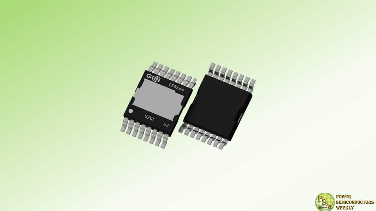
Navitas Semiconductor announced that its high-power GaNSafe family is now available in a TOLT (Transistor Outline Leaded Top-side cooling) package.
The GaNSafe family has been specifically created to serve demanding, high-power applications, such as AI data centers, solar/energy storage, and industrial markets. Navitas 4th generation integrates control, drive, sensing, and critical protection features that enable unprecedented reliability and robustness. GaNSafe is the world’s safest GaN with short-circuit protection (350ns max latency), 2kV ESD protection on all pins, elimination of negative gate drive, and programmable slew rate control. All these features are controlled with 4-pins, allowing the package to be treated like a discrete GaN FET, requiring no VCC pin.
The TOLT packaging enhances thermal dissipation through the top side of the package, allowing heat to be dissipated directly to the heatsink (not through the PCBA). This enables the reduction of operating temperature and increases current capability, resulting in the highest level of system power density, efficiency, and reliability.
“With over 200 million units shipped and supplied with a 20-year warranty, Navitas’ highly integrated high-power GaNSafe ICs are proven to deliver performance and reliability while simplifying Design-IN for systems up to 22kW,” says Charles Bailley, Senior Director of Business Development. “As the most protected, reliable, and safe GaN devices in the industry, GaNSafe took our technology into mainstream applications above 1kW. Now, with the enhanced thermal dissipation of the TOLT package, we are enabling customers to deliver even better performance, efficiency, power density, and reliability in even the most demanding applications.”
Suitable for applications from 1 kW to 22 kW, 650 V GaNSafe in TOLT packaging is available with a range of RDS(ON)MAX from 25 to 98 mΩ. Integrated features and functions include:
- High-speed short-circuit protection, with autonomous ‘detect and protect’ with ultra-fast 350 ns / 50 ns latency.
- Protected, regulated, integrated gate-drive control, with zero gate-source loop inductance for reliable high-speed 2 MHz switching capability to maximize application power density.
- Electrostatic discharge (ESD) protection of 2 kV, compared to zero for discrete GaN transistors.
- 650 V continuous, and 800 V transient voltage capability for extraordinary application conditions.
- Integrated Miller Clamp (no negative gate bias, higher 3rd quadrant efficiency)
- Programmable turn-on and turn-off speeds (dV/dt) to simplify EMI regulatory requirements.
- Simple 4-pin device, allowing the package to be treated like a discrete GaN and requiring no additional VCC pin
- Robust, thermally enhanced packaging: ultra-low RQ_JUNC-AMB and board-level thermal cycling (BLTC) Reliability
In addition to the new ICs, Navitas will be offering reference design platforms based on GaNSafe TOLT for applications including data center power supplies and EV on-board chargers. These system platforms include complete design collateral with fully tested hardware, embedded software, schematics, bill-of-materials, layout, simulation, and hardware test results.
Original – Navitas Semiconductor
-
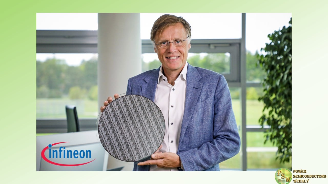
Infineon Technologies AG announced that the company has succeeded in developing the world’s first 300 mm power gallium nitride (GaN) wafer technology. Infineon is the first company in the world to master this groundbreaking technology in an existing and scalable high-volume manufacturing environment. The breakthrough will help substantially drive the market for GaN-based power semiconductors.
Chip production on 300 mm wafers is technologically more advanced and significantly more efficient compared to 200 mm wafers, since the bigger wafer diameter fits 2.3 times as many chips per wafer.
GaN-based power semiconductors find fast adoption in industrial, automotive, and consumer, computing & communication applications, including power supplies for AI systems, solar inverters, chargers and adapters, and motor-control systems. State-of-the art GaN manufacturing processes lead to improved device performance resulting in benefits in end customers’ applications as it enables efficiency performance, smaller size, lighter weight, and lower overall cost. Furthermore, 300 mm manufacturing ensures superior customer supply stability through scalability.
“This remarkable success is the result of our innovative strength and the dedicated work of our global team to demonstrate our position as the innovation leader in GaN and power systems,” said Jochen Hanebeck, CEO of Infineon Technologies AG. “The technological breakthrough will be an industry game-changer and enable us to unlock the full potential of gallium nitride. Nearly one year after the acquisition of GaN Systems, we are demonstrating again that we are determined to be a leader in the fast-growing GaN market. As a leader in power systems, Infineon is mastering all three relevant materials: silicon, silicon carbide and gallium nitride.”
Infineon has succeeded in manufacturing 300 mm GaN wafers on an integrated pilot line in existing 300 mm silicon production in its power fab in Villach (Austria). The company is leveraging well-established competence in the existing production of 300 mm silicon and 200 mm GaN. Infineon will further scale GaN capacity aligned with market needs. 300 mm GaN manufacturing will put Infineon in a position to shape the growing GaN market which is estimated to reach several billion US-Dollars by the end of the decade.
This pioneering technological success underlines Infineon’s position as a global semiconductor leader in power systems and IoT. Infineon is implementing 300 mm GaN to strengthen existing and enabling new solutions and application fields with an increasingly cost-effective value proposition and the ability to address the full range of customer systems. Infineon will present the first 300 mm GaN wafers to the public at the electronica trade show in November 2024 in Munich.
A significant advantage of 300 mm GaN technology is that it can utilize existing 300 mm silicon manufacturing equipment, since gallium nitride and silicon are very similar in manufacturing processes. Infineon’s existing high-volume silicon 300 mm production lines are ideal to pilot reliable GaN technology, allowing accelerated implementation and efficient use of capital. Fully scaled 300 mm GaN production will contribute to GaN cost parity with silicon on R DS(on) level, which means cost parity for comparable Si and GaN products.
300 mm GaN is another milestone in Infineon’s strategic innovation leadership and supports Infineon’s mission of decarbonization and digitalization.
Original – Infineon Technologies
-

JEDEC Solid State Technology Association announced the publication of JEP200: Test Methods for Switching Energy Loss Associated with Output Capacitance Hysteresis in Semiconductor Power Devices. Developed jointly by JEDEC’s JC-70.1 Gallium Nitride and JC-70.2 Silicon Carbide Subcommittees, JEP200 is available for free download from the JEDEC website.
Proliferation of soft switching power conversion topologies brought about the need to accurately quantify the energy stored in a power device’s output capacitance because the energy impacts efficiency of power converters. JEP200, developed in collaboration with academia, addresses the critical power supply industry need to properly test and measure the switching energy loss due to the output capacitance hysteresis in semiconductor power devices and details tests circuits, measurement methods, and data extraction algorithms. The document applies not only to wide bandgap power semiconductors such as GaN and SiC, but also silicon power transistors and diodes.
“Professionals in high-frequency power conversion systems have long sought a standardized approach to testing new switching energy losses,” said Dr. Jaume Roig, Member of Technical Staff, onsemi and Vice Chair of the JC-70 Committee. “This document now provides helpful guidance on testing energy losses related to output capacitance hysteresis caused by displacement currents. With this clarity, system optimization can proceed more accurately.”
“JEDEC’s JC-70 committee has the expertise necessary to meet the demands of the entire power semiconductor industry, and the development of JEP200 demonstrates how the JEDEC process enabled the committee to swiftly respond to an industry need,” said John Kelly, JEDEC President. “JEP200 encompasses GaN, SiC, and Si power devices, helping the industry navigate design challenges caused by the growing number of new power conversion topologies.”
Original – JEDEC
-

EPC will participate in PCIM Asia 2024. The event will take place from August 28-30 in Shenzhen, China. Attendees are invited to visit EPC at Hall 11, Stand F01 to explore the industry’s most comprehensive portfolio of GaN power conversion solutions.
See How GaN is Powering the Future
GaN power semiconductors are used in fast-charging applications for consumer electronics, aerospace and defense applications, satellites, high density AI servers, drones, robots, autonomous vehicles, telecommunications equipment and medical electronics, among other innovative technologies.
- AI servers, critical for processing vast amounts of data in real-time, require power-efficient and high-speed electronics that GaN technology can deliver.
- Humanoid robotics require lightweight, compact, and highly responsive components. GaN enables more agile and intelligent robots that can perform complex tasks with greater precision.
- The shift toward electric vehicles (EVs) and advanced driver-assistance systems (ADAS) requires power solutions that are not only highly efficient but also capable of handling the increased power demands. GaN’s superior efficiency, compactness, and thermal performance make it the ideal choice for powering the future of transportation.
EPC is uniquely positioned to support these markets with its pioneering GaN technology. EPC’s innovative solutions not only offer superior performance but also drive advancements in these critical sectors, enabling businesses to realize their full potential in a rapidly evolving technological landscape.
Visit EPC at PCIM Asia to discover how EPC’s GaN technology can power your next breakthrough—stop by the booth to explore our latest innovations and speak with our experts.
Explore Booth (Hall 11, Stand F01)
At the EPC booth, visitors will experience firsthand how GaN FETs and ICs enable higher efficiency, smaller size and weight, and lower costs in applications such as DC-DC converters for high power density AI servers, motor drives for eMobility, robotics, and drones, and more.
- Use the Interactive Wall of GaN to select the ideal GaN FET or IC for your application
- Connect with EPC’s team of experts to gain insight into the ‘GaN First Time Right™ Design Process. Attendees will gain valuable knowledge and tools to enhance their projects and drive efficiency to new levels.
- Meet the Robots: “Chip”, the robot dog, and his robotic friends demonstrate GaN-based DC-DC, lidar, and motor drive solutions for advanced robotics.
Schedule a Meeting: Learn from GaN Experts and discover strategies to optimize your power systems. To schedule a meeting during PCIM Asia contact renee.yawger@epc-co.com
Conference Sessions: Attend technical sessions to gain insights from industry leaders into the latest trends and advancements in GaN power conversion technology.
- The Future of Untethered Robotics: GaN-Powered Solutions for Mobility, AI, and Machine Vision
Presenter: Alex Lidow, Ph.D. - Comprehensive Board Level Temperature Cycling Lifetime Projection of WLCSP GaN Power Devices
Presenter: Shengke Zhang, Ph.D. - Comparison of Board-side and Back-side Thermal Management Techniques for eGAN® FETs in a Half-Bridge Configuration
Presenter: Adolfo Herrera, Ph.D. - Validating Duty Cycle-Based Repetitive Gate and Drain Transient Overvoltage Specifications for GaN HEMTsHost: Bodo’s Power Systems
Presenter: Shengke Zhang, Ph.D.
“We are thrilled to participate in PCIM Asia and showcase our cutting-edge GaN technology”, said Nick Cataldo, VP of Sales and Marketing at EPC. “We look forward to demonstrating how our solutions are transforming industries by enabling higher efficiency, smaller size, and lower costs.”
Original – Efficient Power Conversion
-

SweGaN AB, a European semiconductor manufacturer that develops and produces custom engineered Gallium Nitride on Silicon Carbide (GaN-on-SiC) epitaxial wafers, reported orders for its benchmark QuanFINE® epiwafers worth 17 MSEK in the first half of 2024, including three large frame agreements from undisclosed major Telecom and Defense market players. The company reported a 100% YoY order increase and began deliveries from its new facility in Linköping, Sweden, marking significant progress in its scale-up journey.
In additional notable news, the semiconductor manufacturer announces a newly completed QuanFINE epiwafer customer qualification with a device manufacturer.
In the last two years, SweGaN has displayed an exciting operational transformation in alignment with its growth strategy and global demands for GaN-on-SiC epiwafers. Securing a Series A investment round, the company has scaled its organization, established a streamlined team, and deployed a new high-capacity production facility to drive its growth strategy and future KPIs.
– “Today we celebrate three significant milestones that signal SweGaN’s transition from a pure R&D company to a rigorous global semiconductor manufacturer.” says Dr. Jr-Tai Chen, CEO at SweGaN.
– “Currently, there is a strong momentum in the Telecom industry to upgrade technology from 5G to 5G Advanced, continues Chen. SweGaN’s patented QuanFINE® buffer-free GaN-on-SiC material is well-suited to meet the demanding technical requirements of the new technology, particularly in terms of device efficiency and thermal management. This applies to the new Telecom standard 5G Advanced, as well as the strong demands for enhanced sensing capability in Defense applications. The new framework orders will accelerate product development and production ramp-up enabling SweGaN to tap the market opportunities in both the Telecom and Defense sectors.”
With SweGaN’s new production facility in full swing, the company has the tools to fully embrace its ambitious scale-up strategy and significantly boost manufacturing capacity of next-generation GaN-on-SiC engineered epitaxial wafers. Simultaneously, the company aims to continue to innovate through new R&D initiatives and deepen partnerships with suppliers and customers to establish resilient supply chains.
– “I take immense pride in our synergistic team, in both successfully qualifying SweGaN’s first epiwafer product with a device manufacturer and executing on the significant undertaking of bringing the the new high-capacity wafer production facility into operation, from planning to deployment,” continues Chen.
Original – SweGaN
-
DCDC converters are essential in any electric or hybrid vehicle to connect the high-voltage battery to the low-voltage auxiliary circuits. This includes 12 V power headlights, interior lights, wiper and window motors, fans, and at 48 V, pumps, steering drives, lighting systems, electrical heaters, and air conditioning compressors. In addition, the DCDC converter is important for developing more affordable and energy-efficient vehicles with an increasing number of low voltage functions.
According to TechInsights, the global automotive DC-DC converter market size was valued at USD 4 billion in 2023 and is projected to grow to USD 11 billion by 2030, exhibiting a CAGR of 15 percent during the forecast period. Gallium nitride (GaN) in particular plays a crucial role here, as it can be used to improve the power density in DCDC converters and on-board chargers (OBC).
For this reason, Vitesco Technologies, a leading supplier of modern drive technologies and electrification solutions, has selected GaN to improve the power efficiency of its Gen5+ GaN Air DCDC converter. The CoolGaN™ Transistors 650 V from Infineon Technologies AG significantly improve the overall system performance while minimizing system cost and increasing ease of use. As a result, Vitesco created a new generation of DCDC converters that set new standards in power density (efficiency of over 96%) and sustainability for power grids, power supplies, and OBCs.
The advantages of GaN-based transistors in high-frequency switching applications are considerable, but even more important is the high switching speed, which has been increased from 100 kHz to over 250 kHz. This enables very low switching losses, even in hard-switched half-bridges, with minimized thermal and overall system losses.
In addition, Infineon’s CoolGaN Transistors feature high turn-on and turn-off speeds and are housed in a top-cooled TOLT package. They are air-cooled, eliminating the need for liquid cooling and thereby reducing overall system costs. The 650 V devices also improve power efficiency and density, enabling an output of 800 V. In addition, they feature an ON-resistance (R DS(on)) of 50 mΩ, a transient drain-to-source voltage of 850 V, an I DS,max of 30 A, and an I DSmax,pulse of 60 A.
“We are delighted to see industry leaders like Vitesco Technologies using our GaN devices and innovating with their applications,” said Johannes Schoiswohl, Senior Vice President & General Manager, GaN Systems Business Line Head at Infineon. “The ultimate value of GaN is demonstrated when it changes paradigms, as in this example of moving from a liquid-cooled system to an air-cooled system.”
With GaN Transistors, Vitesco Technologies was able to design its Gen5+ GaN Air DCDC converters with passive cooling, which reduces the system’s overall cost. The GaN devices also allow for simplified converter design and mechanical integration. As a result, the DCDC converters can be flexibly positioned in the vehicle, reducing the workload for manufacturers.
The use of GaN also allows the power of the converters to be scaled up to 3.6 kW and the power density to be increased to over 4.2 kW/l. The Gen5+ GaN Air DCDC converters offer an efficiency of over 96 percent and improved thermal behavior compared to the Gen5 Liquid-Cooled converters. They provide a two-phase output of 248 A at 14.5 V continuous.
The phases can be combined to achieve the maximum output power. Still, it is also possible to switch off one phase under partial load conditions and interleave the switching frequency between the two phases. In addition, by switching the input of two phases in series, the converters based on the CoolGaN power transistors 650 V can be used to implement 800 V architectures without exceeding the maximum blocking voltage of the device. The converters also feature an isolated half-bridge topology consisting of a GaN-based half-bridge, a fully isolated transformer, and an active rectifier unit for each phase.
Original – Infineon Technologies
-

Navitas Semiconductor announced that Samsung had expanded adoption of Navitas’ GaNFast ICs from the original flagship Galaxy S22, S23 and S24 to the mainstream Galaxy A, and revolutionary Galaxy Z Fold6 and Galaxy Z Flip6 smartphones with enhanced Galaxy AI features.
GaN runs up to 20x faster than legacy silicon and enables chargers up to 3x more power and 3x faster charging in half size and weight. GaNFast power ICs enable high-frequency, high-efficiency power conversion, achieving up to a 50% shrink vs. prior designs.
The new 25W charger (EP-T2510) features new energy-saving technology to reduce standby losses by 75% to only 5 mW, which aligns with Navitas’ environmental advances, where every GaNFast IC saves 4 kg of CO2 vs. legacy silicon chips.
“Since enabling the world’s first production GaN charger in 2018, Navitas has pioneered and leads the adoption of GaN to replace legacy silicon chips,” noted David Carroll, Sr. VP Worldwide Sales for Navitas. “Our production partnership with Samsung dates back to the Galaxy S22 Ultra, and today’s announcement reflects the dramatic expansion of GaN from niche, flagship designs to adoption in high-volume, mainstream phones.”
Original – Navitas Semiconductor
