-

AIXTRON SE supports Nexperia B.V. in the ramp-up of its 200mm volume production for silicon carbide (SiC) and gallium nitride (GaN) power devices. With the new G10-SiC for the 200mm SiC volume ramp, Nexperia is placing a repeat order for AIXTRON SiC tools. This is complemented by an order for AIXTRON G10-GaN tools.
Both GaN and SiC epitaxial films are essential for the design of next-generation energy-efficient Field-Effect (FET) or Metal-Oxide-Field Effect (MOSFET) transistors to be used in various power conversion applications ranging from data centers and solar inverters in electric vehicles (EV) or trains.
Nexperia has decades of experience in the development of power devices, achieving more than 2.1 billion USD in revenue in 2023. After releasing its first GaN FET device in 2019 and its first SiC MOSFET in 2023, Nexperia continues to expand its portfolio with new high-reliability and power-efficient devices.
Nexperia, headquartered in Nijmegen (Netherlands), operates front-end factories in Hamburg (Germany) and Greater Manchester (England). The AIXTRON epitaxy systems will be installed at Nexperia’s wafer fab in Hamburg (Germany), further strengthening the semiconductor production capabilities in the region. Nexperia’s Hamburg site produces approximately 100 billion discrete semiconductors annually, accounting for about a quarter of the global production of this type of products.
“We are honored to strengthen our alliance with Nexperia, a pivotal player in the semiconductor landscape. Our G10 epitaxy solutions are at the heart of this collaboration, bolstering Nexperia’s growth strategies and enabling the high-volume production of wide bandgap semiconductors for commercial applications. Together, we are setting the pace for the industry’s transition to more energy-efficient SiC and GaN solutions”, said Dr. Felix Grawert, CEO and President of AIXTRON SE.
“As we advance our technological capabilities and market presence in high-power semiconductor production, our strategic partnership with AIXTRON is transformative. Integrating the G10 systems will significantly enhance our wide bandgap technology development and production capabilities. We build on AIXTRON’s proven uniformity and leverage the additional productivity gains of AIXTRON’s G10 tools to scale up our production efficiently and cost-effectively. With the new G10 tools in our Hamburg facility, we are poised for further advancements in our production capabilities,” said Achim Kempe, COO at Nexperia B.V.
Original – AIXTRON
-

As part of a so-called Joint Lab at Fraunhofer IISB, AIXTRON SE operates equipment, works on process development for SiC epitaxy and runs a demo center for its customers. Joint Labs like this are a great opportunity for companies to collaborate with Fraunhofer IISB in an industry-compatible laboratory environment.
For the epitaxy Joint Lab, the awarded IISB team ensures the continuous fault-free operation of already 5 state-of-the-art G10 SiC reactors, and enables the installation of new systems with minimal downtime. By setting up automated metrology and by optimizing wafer logistics, workflows and data management, the team has also established a modern wafer characterization facility at the IISB with a fast feedback loop for AIXTRON.
Fraunhofer IISB is thrilled for its colleagues Rainer Apelt, Nino Fröbisch and Katharina Roßhirt-Lilla from the SiC Epitaxy Group of the Materials Department together with Christian Heilmann, Rainer Schönweiß and Christopher Torscher from the Infrastructure Group within the Central Services Department. Such outstanding results are the base for the success of the Joint Labs model at Fraunhofer IISB.
Original – Fraunhofer IISB
-
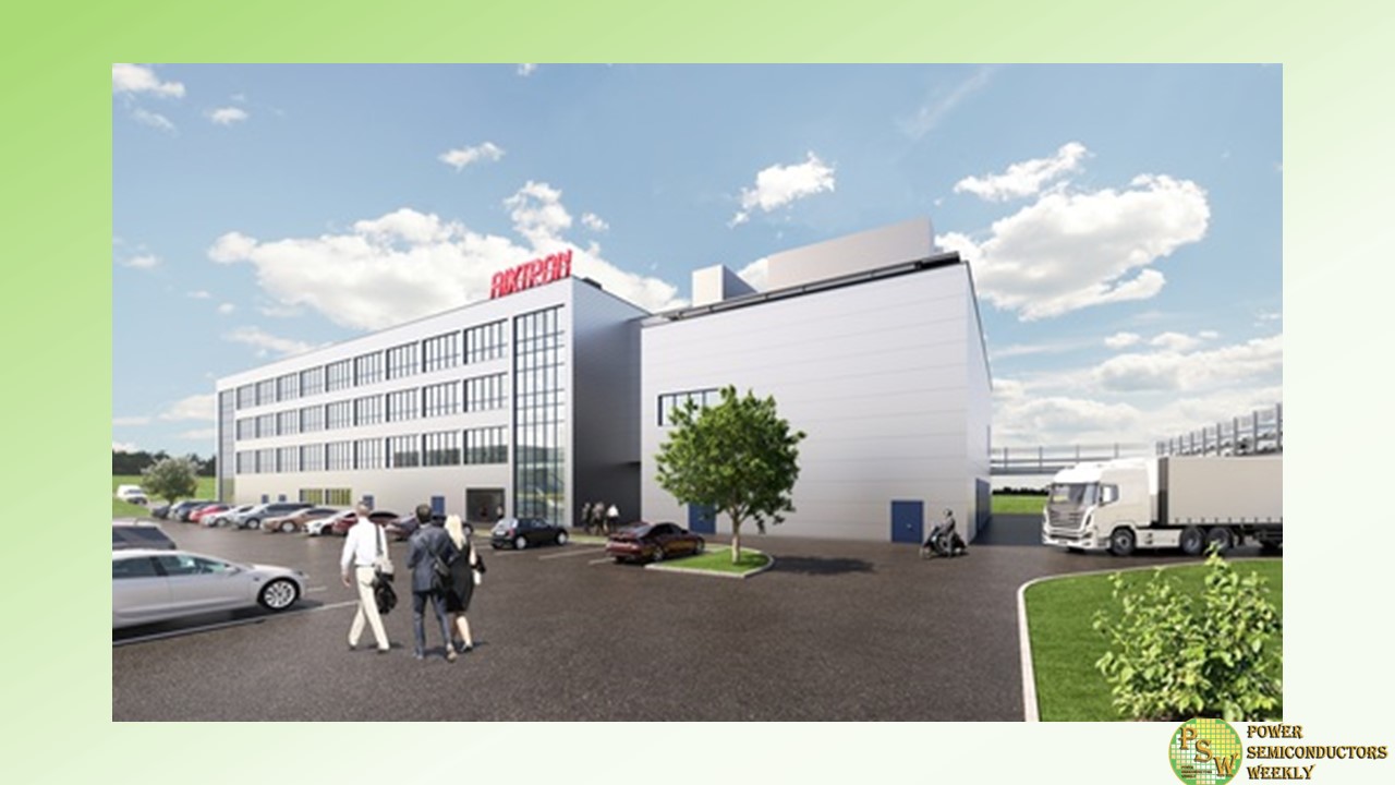
AIXTRON SE has officially started the construction of the new innovation center at its headquarters in Herzogenrath, Germany. The leading provider of deposition equipment to the semiconductor industry is investing around EUR 100 million in 1000m2 of clean room with additional space for the required metrology equipment.
This research facility will feature the latest technologies available in the industry. The first systems are scheduled to move into the new building during the second half of 2024. The official handover is planned for early 2025.
This milestone in the company’s successful history was marked with a symbolic ground-breaking ceremony attended by representatives from politics, science and research as well as key suppliers of the company. The framework for this significant step was a celebration in honor of AIXTRON’s 40th year since its founding: The company started in December 1983 as a spin-off from RWTH Aachen University.
Since that time, AIXTRON has always been at the forefront of innovation and new, groundbreaking semiconductor technologies. The new innovation center continues on this path and forms an important foundation for the company’s continued successful growth.
“We have just completely renewed our portfolio with our successful G10 product family. The demand from our customers is already very high, so we are in the middle of a volume ramp. And we are now also starting to work on the next generation of innovative technical solutions. With this, we will successfully drive forward the electrification of the world with the megatrends of digitalization, electromobility, and energy efficiency. The new innovation center provides us with essential capacities for all of this,” says Dr. Felix Grawert, CEO of AIXTRON SE.
The cleanroom area of the innovation center will be of class ISO 6, expandable up to ISO 4. The new complex, known in the industry as “fab”, will be one of the most compact and complex semiconductor fabs in the world: the area has two sub-levels. The first sub-level accommodates, e.g., the pump filter cabinets of the systems while the facility level houses all supporting processes and systems for the entire infrastructure.
This type of space utilization increases cleanroom efficiency by a factor of up to three compared to the previously used cleanroom areas.
Original – AIXTRON
-
AIXTRON SE enables the semiconductor foundry BelGaN to expand its business into the growing GaN marketand to accelerate GaN technology innovation. For this important strategic step, BelGaN relies on AIXTRON’s new G10-GaN, which offers best-in-class performance, an all-new compact design, and overall lowest cost per wafer.
Starting with an 8x150mm configuration, the system will be delivered to the BelGaN production site in Oudenaarde (Belgium) before the end of 2023 and will in the future migrate to 5x200mm.
BelGaN, a leading GaN (Gallium Nitride) automotive-qualified semiconductor open foundry in Europe, recently announced the production start of its first generation 650V eGaN technology. The Gen1 platform is designed for the requirements of energy-efficient applications for sustainability and carbon neutrality.
The G10-GaN will be used to further extend the range of power chips with voltage ratings from 40V to 1200V, using GaN-on-Si, GaN on SOI, and novel GaN-on-engineered substrates. It will be applied both on lateral as well as vertical power-GaN products, with a focus on high performance, automotive quality and reliability, high yield, and low costs.
“GaN-epitaxy using MOCVD is a most critical process in any power-GaN technology, both to innovate device architectures, boost performance, yield, and quality, and to cut down the cost of GaN products. This drives a paradigm shift in power electronics, opening up fast-growing markets in e-mobility, datacom, energy conversion, etc., on a road to an electrified, carbon-neutral society.
We have been impressed by the high levels of productivity, uniformity, and low cost of ownership of AIXTRON’s new G10 platform. We highly value AIXTRON’s technological advance, leadership, and continuous innovation. The proximity of AIXTRON, in the midst of the GaN ValleyTM ecosystem, and the collaboration with its team is essential for us to rapidly achieve our innovation and production objectives,” says Dr Marnix Tack, CTO and Vice President Business Development of BelGaN.
“We are very proud that BelGaN chose AIXTRON and our latest innovative powerhouse, the G10-GaN, for the important strategic milestone to add GaN epitaxy to its existing GaN processing line in Oudenaarde (Belgium). Currently, GaN power devices are rapidly adopted in a wide range of applications, and many customers are adding GaN capabilities to their silicon lines. We are excited that technology made by AIXTRON is facilitating this important transition,” says Dr. Felix Grawert, CEO and President of AIXTRON SE.
The all-new G10-GaN cluster solution builds on the fundamentals of AIXTRON’s current tool of record, the G5+ C, while extending each single performance metric:the new platform delivers twice the productivity per cleanroom area while enabling a new level of material uniformities, unlocking new levers of competitiveness for AIXTRON’s customers.
They benefit from more than 25% lowest cost of ownership than with any other equipment on the market today. The G10-GaN also guarantees the highest throughput per m2/cleanroom, and with its full automation end-to-end, it is the only MOCVD system fully designed for silicon fabs.
Original – AIXTRON
-
AIXTRON SE supports GlobiTech Inc., one of the world’s largest silicon-epitaxy foundries, to expand their business into silicon carbide (SiC) epitaxy. AIXTRON’s new G10-SiC has enabled this global leader to quickly ramp its SiC epitaxy production into high volume to address the world’s increasing demand for power epi-wafers. GlobiTech’s selection of the G10-SiC means a future-proof investment based on dual wafer size configuration of 9×150 & 6×200 mm and the highest throughput per fab space available in the SiC industry today.
The G10-SiC was officially introduced in September 2022. And it has quickly become the tool of record for both 150mm and 200mm SiC device makers as well as foundries like GlobiTech, the wholly owned subsidiary of GlobalWafers Co., Ltd., which manufactures silicon carbide and silicon epitaxial wafers focused on power and electric vehicle (EV) market segments.
“When one of the largest manufacturers and foundries like GlobiTech diversifies its business, it is a clear signal of a long-lasting trend in the semiconductor industry: conventional silicon is being replaced by silicon carbide in an ever-increasing number of applications. And it makes us proud when a leading company such as GlobiTech chooses AIXTRON and our new G10-SiC as an enabler of its transition intothis emerging SiC market. It confirms our overall strategy and the prospects for further growth”, says Dr. Felix Grawert, CEO and President of AIXTRON SE.
GlobiTech, located in Sherman, TX, is already in high-volume production using both G5WW C and G10-SiC AIXTRON systems, with continued installation capacity over the next years.Modeled after the silicon business, GlobiTech supplies both SiC substrates and SiC epitaxy to the market.
“In AIXTRON, we have found a strong partner supporting us in our vision and plans to expand our business into the SiC epitaxy market – an important step as SiC technology is one of the fastest-growing semiconductor sectors. AIXTRON tools allow us to get the most wafers out of our current fab. And AIXTRON’s team understands what it takes to compete against silicon to grow this market while offering great customer support and service”, says Mark England, President of GlobalWafers.
The G10-SiC is the first SiC epitaxy tool on the market that truly enables high-volume production of SiC epi-wafers. Since the G10-SiC offers both 9×150 mm and 6×200 mm batch configurations, it is an instrumental tool for a market rapidly transitioning from 6-inch (150mm) to 8-inch (200 mm) wafer diameters. The new platform is built around AIXTRON’s proven automated wafer cassette-to-cassette loading solution with high-temperature wafer transfer.
Combined with high growth rate process capabilities, the G10-SiC provides best-in-class wafer throughput, an excellent epi wafer performance in terms of quality and uniformity, and the best throughput per square meter of fab space. All this leads to the lowest cost of ownership in the market. It is estimated that in 2023, the new G10-SiC will become AIXTRON’s top-selling product.
The wide-bandgap material SiC is set to become mainstream technology for efficient power electronics. Driven by the growing adoption of SiC-based power semiconductors within e-mobility solutions and the overall acceleration of the charging infrastructure, the global demand for SiC wafers is growing rapidly.And with its superior characteristics, SiC semiconductors offer higher energy efficiency than conventional power electronics based on silicon. Therefore, SiC significantly contributes to reducing the global CO2 footprint.
Original – AIXTRON
-
AIXTRON SE plans to invest up to 100 million euros at its Herzogenrath site. A new innovation center is to be built, which will provide the manufacturer of deposition equipment to the semiconductor industry with enhanced capacities for research and development. AIXTRON received approval for the new project from the company’s Supervisory Board.
The new innovation center will provide 1000m2 of cleanroom space and will be built on the company’s premises in Herzogenrath, Germany. The new building will create further capacities for the next product generations which are already in preparation, as well as for further product developments beyond that.
“With our products, we address the megatrends of digitalization, electromobility and energy efficiency and are experiencing a strong and steadily growing demand. Technical innovations and product developments that precisely address the needs of our customers are the key to our success. And our dynamic environment offers us further growth opportunities,” says Dr. Felix Grawert, CEO of AIXTRON SE. “We are therefore very pleased that the Supervisory Board has approved this project which will enable us to create the foundation for further product developments and for future growth.”
The importance of product development in the dynamic semiconductor industry is demonstrated by the success of AIXTRON’s new “G10” system generations. In the first year after market introduction, AIXTRON expects to generate more than 40 percent of its annual revenues with this new product generation. Right after its official launch, the new tool for the silicon carbide material system (G10-SiC) has already generated a high order intake. And it is expected to continue to drive further growth all throughout 2023 and beyond.
Also, the new AIXTRON solution for the gallium-arsenide/indium-phosphite material system (G10-AsP) which was launched at the beginning of 2023 already enjoys a strong demand. For the first time, it enables the high-volume production of Micro LEDs and photonic components such as lasers on wafers with a diameter of up to 200mm. Later in the year, the new G10 system for gallium nitride (GaN) will also be launched. The material systems SiC and GaN have the potential to fully cover the complete range of power electronics, from electromobility to renewable energy technologies to fast data transmission. With their outstanding material properties, they will ensure a significant reduction in global CO2 emissions in these areas and help electromobility achieve a breakthrough.
Original – AIXTRON
