-
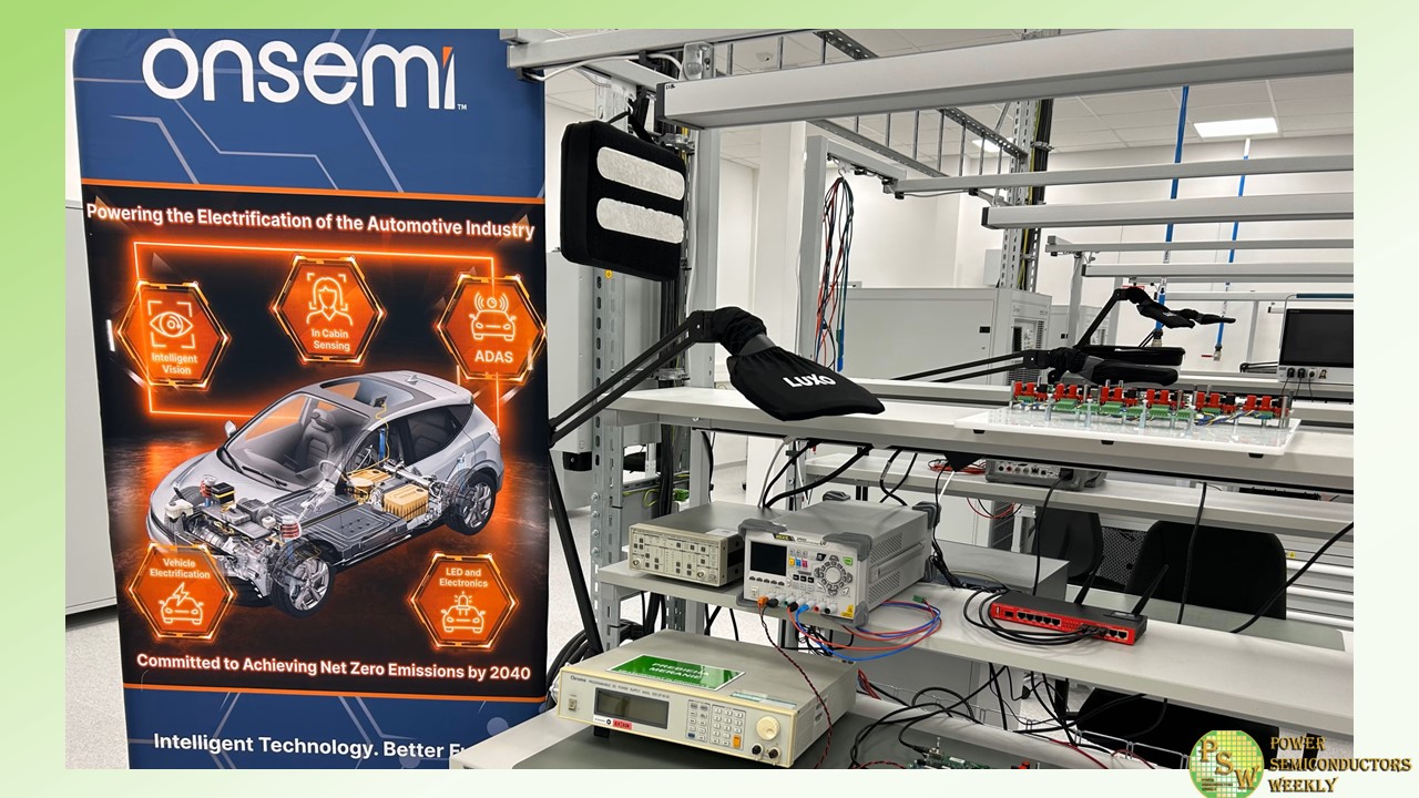
onsemi opened an application test lab in Piestany, Slovakia, focused on the advancement of system solutions for battery/plug-in hybrid/electric vehicles (xEVs) and energy infrastructure (EI) power conversion systems. The state-of-the-art systems applications lab provides specialized equipment to develop and test next-generation silicon (Si) and silicon carbide (SiC) semiconductor solutions in collaboration with automotive OEMs, Tier 1s and EI providers.
Modern semiconductor devices are essential for highly efficient power conversion in xEV powertrains and charging, as well as applications in renewable energy. The new lab will play a central role in ensuring that the development of future power products results in highly differentiated, value-add solutions tailored to customers’ specific requirements.
The new facility consists of two high-voltage power labs that focus on systems and device level development as well as evaluation of SiC/Si traction inverters and ACDC/DCDC power converters. Laser welding facilities, mechanical clean rooms and workshops further enable fast prototyping and testing of next-generation system solutions.
Evaluation capabilities for the next-generation system solutions include:
- Continuous 24/7 testing
- Internally developed and patented software and hardware solutions to support high-voltage power cycling via space vector modulation (SVM) and sinusoidal pulse width modulation (SPWM)
- High-accuracy logging devices for assessing SiC and Si health and reliability
- Simulation of the harsh conditions faced by inverters during operation, testing liquid-cooled devices at temperatures as low as minus 50 degrees C and up to 220 degrees C
- Wider range of industry-recognized software allows for the programing of FPGAs and ARM microcontrollers on site, as well as qualification testing, data analysis and 3D modeling
Original – onsemi
-
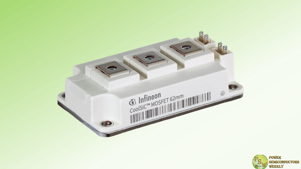
Infineon Technologies AG announced the expansion of its CoolSiC 1200 V and 2000 V MOSFET module families with a new industry-standard package. The proven 62mm device is designed in half-bridge topology and is based on the recently introduced and advanced M1H silicon carbide (SiC) MOSFET technology.
The package enables the use of SiC for mid-power applications from 250 kW – where silicon reaches the limits of power density with IGBT technology. Compared to a 62mm IGBT module, the list of applications now additionally includes solar, server, energy storage, EV charger, traction, commercial induction cooking and power conversion systems.
The M1H technology enables a significantly wider gate voltage window, ensuring high robustness to driver and layout-induced voltage spikes at the gate without any restrictions even at high switching frequencies. In addition to that, very low switching and transmission losses minimize cooling requirements.
Combined with a high reverse voltage, these devices meet another requirement of modern system design. By using Infineon’s CoolSiC chip technology, converter designs can be made more efficient, the nominal power per inverter can be increased and system costs can be reduced.
With baseplate and screw connections, the package features a very rugged mechanical design optimized for highest system availability, minimum service costs and downtime losses. Outstanding reliability is achieved through high thermal cycling capability and a continuous operating temperature (T vjop) of 150°C. The symmetrical internal package design provides identical switching conditions for the upper and lower switches. Optionally, the thermal performance of the module can be further enhanced with pre-applied thermal interface material (TIM).
The CoolSiC 62mm package MOSFETs are available in 1200 V variants of 5 mΩ/180 A, 2 mΩ/420 A and 1 mΩ/560 A. The 2000 V portfolio will include the 4 mΩ/300 A and 3 mΩ/400 A variants. The portfolio will be completed in Q1 2024 with the 1200 V/3 mΩ and 2000 V/5 mΩ variants.
An evaluation board is available for rapid characterization of the modules (double pulse/continuous operation). For ease of use, it provides flexible adjustment of the gate voltage and gate resistors. At the same time, it can be used as a reference design for driver boards for volume production.
Original – Infineon Technologies
