-
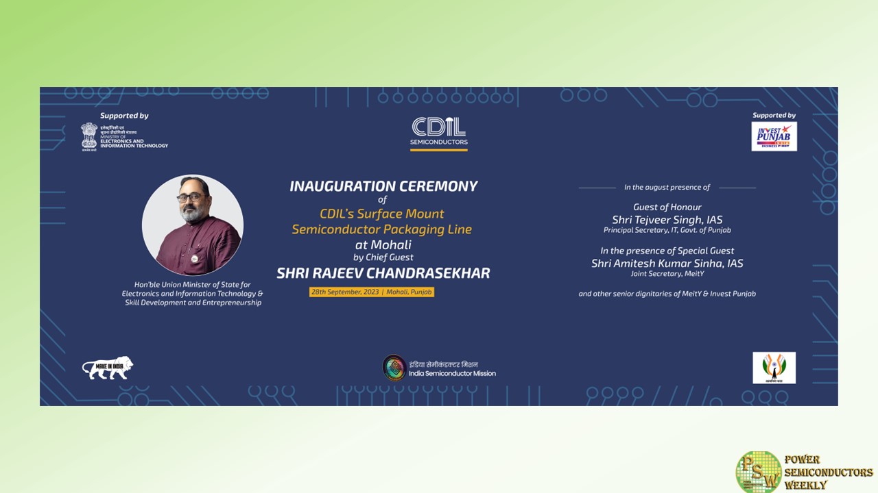
Hon’ble Union Minister of State for Electronics and Information Technology, Shri Rajeev Chandrasekhar, virtually inaugurated the new Surface Mount Semiconductor Packaging Line, at Continental Device India Private Limited’s (CDIL) Mohali plant today. With the new versatile SMA and SMB package line, via the Government of India’s SPECS, CDIL becomes India’s first Silicon Carbide components manufacturer, scaled to make auto-grade devices, including Silicon Carbide MOSFETs, Silicon Carbide Schottky Diodes, Rectifiers, Zeners and TVS Diodes among others for the global as well as the domestic market. The expansion of assembly lines will increase CDIL’s total capacity at the facility to 600 million units annually.
The new line inauguration was also attended by Shri Tejveer Singh, IAS, Principal Secretary, IT, Government of Punjab, and Shri Amitesh Kumar Sinha, IRAS, Joint Secretary, MeitY and other senior dignitaries of MeitY and Invest Punjab.
With the impending surge in electric vehicles (EVs), power management devices and solar-powered panels, globally as well as in India, and their increased reliance on wide band gap electronics, CDIL identified and laid focus on Silicon Carbide (SiC) products.
SiC is an emerging technology that allows for much-improved efficiencies and power-handling capabilities, especially in high-power charging applications and battery management systems. CDIL spent R&D efforts pursuing SiC technology so as to build proficiency and assist in the world’s switch to Electric Vehicles.
Expressing his gratitude, Tejveer Singh, IAS, Principal Secretary, IT, Government of Punjab, said, “I am very very thankful to the CDIL team for this great effort in expanding the plant capacity and assembly line. And as CDIL and SCL sign the MoU, we can finally see Mohali becoming the chip-making hub of India. The Government has a vision to cultivate a dynamic semiconductor ecosystem in Mohali and therefore, the modernization of SCL could provide the sector the much needed impetus to put Mohali on the semiconductor manufacturing map of India.”
Speaking at the launch of the new assembly lines, Amitesh Kumar Sinha, IRAS, Joint Secretary, MeitY, said, “India’s Semiconductor mission is a key focus for both the Union and the State Governments, and there have been many developments in the sector. Yet, India still has much to catch up, with a projected surge in demand to approximately $110 billion by 2030. At MeitY, our objective is to modernise and commercialise SCL with focus on making it a R&D hub for developing the semiconductor ecosystem in the country.
It’s heartening to see CDIL taking the lead in Packaging of discrete semiconductor devices. CDIL has capability for R&D, Design, and Packaging. Earlier, they also had a fabrication facility. I hope CDIL will also consider setting up a discrete fab in the country by availing financial support under the Semicon India programme in future. As CDIL and SCL join hands for knowledge exchange, India can look forward to more indigenous chip manufacturing and packaging for India and the world in the upcoming future.”
CDIL has also established an advanced testing and reliability laboratory at the Mohali plant. The facility, a one-of-a-kind in India, is equipped to meticulously qualify the semiconductor products according to the stringent standards stipulated by the Automotive Electronics Council (AEC), ensuring they meet the rigorous demands of the automotive domain.
Commenting on the same, Prithvideep Singh, General Manager, CDIL said, “In line with our steadfast commitment to innovation and market diversification, CDIL Semiconductors has strategically positioned itself to meet the burgeoning demands of the automotive sector, both within India and on a global scale. Even though SiC devices are notoriously hard to manufacture at scale, we have spent effort and investment to master them. CDIL has been able to innovate on the brittleness and complexity around the production of SiC devices and has earned the resounding approval of large multinational customers in export markets.”
CDIL also signed an MoU with the Semi-Conductor Laboratory (SCL), a research institute in Mohali under MeitY, undertaking research and development in the field of semiconductor technology. Both parties will aim to establish a comprehensive framework wherein SCL’s specialized knowledge and wafer fabrication facilities are utilized to produce indigenized wafers for CDIL’s discrete semiconductor devices, using CDIL’s proprietary manufacturing processes. This collaborative effort is aimed as a significant stride towards advancing India’s semiconductor ambitions in fostering a stronger, self-reliant industry in the region.
Silicon Carbide (SiC) material boasts a significantly wider bandgap compared to traditional semiconductor materials like silicon. A wide bandgap (~3.26 eV for SiC) enables SiC devices to operate at higher temperatures and handle higher breakdown voltages. Consequently, SiC emerges as the optimal choice for the electric vehicle (EV), power management and solar sectors, as it allows semiconductor components to operate reliably in high temperatures, reducing the need for complex cooling systems.
The company has already initiated pilot production in August with 50 million units and promptly delivered its inaugural batch to customers in both the domestic and international markets. CDIL operates manufacturing facilities and a reliability lab in Mohali and Delhi, serving industries with a strong emphasis on the Automotive, Defence, and Aerospace sectors. With 59 years of legacy, a worldwide customer base, with many industry leaders as loyal customers spread throughout the world including China, Brazil, Germany, Hong Kong, Japan, Malaysia, Russia, Singapore, South Africa, South Korea, Turkey, USA and the UK.
Original – CDIL Semiconductors
-
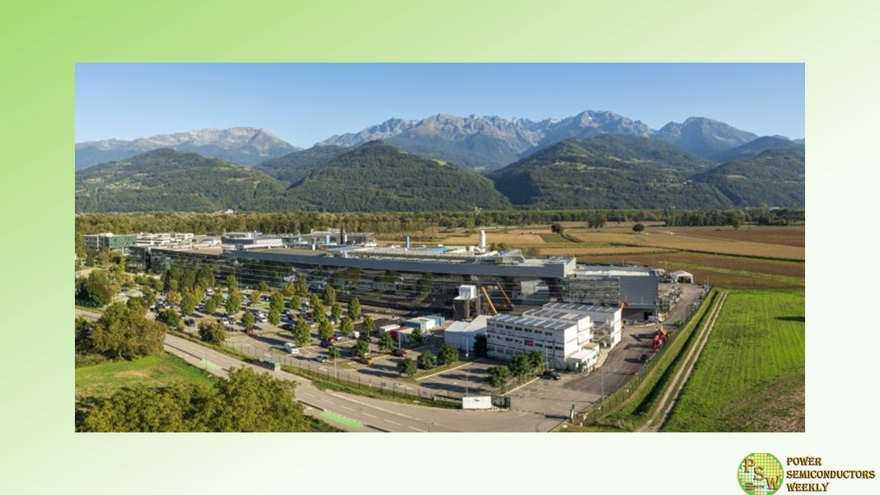
Soitec opened its new plant in Bernin, near Grenoble, in the presence of Thierry Breton, European Commissioner for the Internal Market and Roland Lescure, French Minister Delegate for Industry.
Soitec has developed its SmartSiC™ technology as a response to vehicle electrification challenges.
The technology, based on silicon carbide (SiC), sets a new standard with improved efficiency for energy conversion systems. Thanks to its reduced energy losses, better thermal management and improved power density, the material increases the range and performance of electric vehicles.
Through the application of SmartCut™ technology, each SiC substrate can be used 10 times.
As a result, SmartSiC™ enables electric vehicles to achieve ranges above 500 km, compared with an average 350 km for vehicles using silicon IGBT alternatives – while also reducing CO2 emissions during wafer manufacturing by 70% compared to monocrystalline SiC substrates.
Development of the technology began in 2020 in partnership with CEA-Leti and has received financial support from the French state, the region, local authorities and the European Union.
A new production facility in step with Soitec’s ambition
The new plant will have a 2,500 m2 footprint and a final production capacity of 500,000 SmartSiC™ wafers per year.
It will contribute to Soitec’s strategy of sustainable growth towards a threefold expansion of addressable markets by 2030, reinforcing the company’s leadership position in the strategic semiconductor materials market.
The new plant will lead to the creation of 400 direct jobs, while also reinforcing the attractiveness and dynamism of the “French Silicon Valley” ecosystem.
Pierre Barnabé, Chief Executive Officer of Soitec, stated: “More than ever we are ready to establish our SmartSiC™ technology as a new standard in semiconductor materials for coming generations of electric cars. This plant will enable us to meet growing demand for silicon carbide and achieve a 30% market share by 2030, while helping to make electric mobility more efficient and affordable. Completed in record time, it is the embodiment of our industrial performance and our future-facing strategy, based on the expansion of our product and technology portfolio.
This is also an important day for our region, which is once again showing its dynamic and exemplary approach to industrial innovation, with technologies designed, developed, and manufactured within our ecosystem. We will create jobs and continue to showcase French and European knowhow in global semiconductor markets.”
Original – Soitec
-

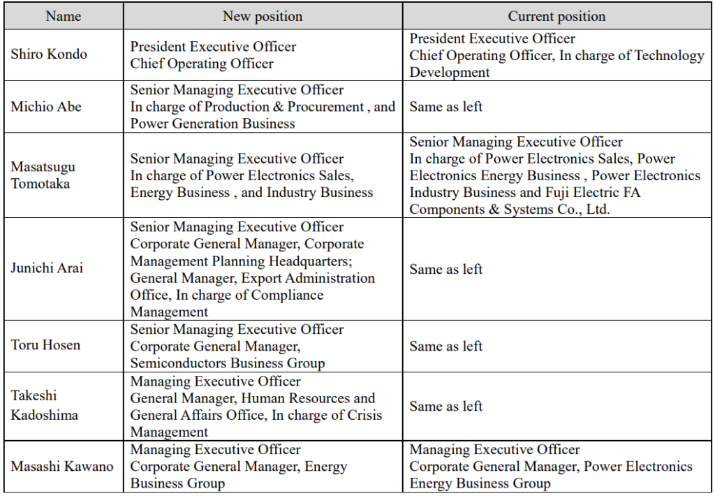
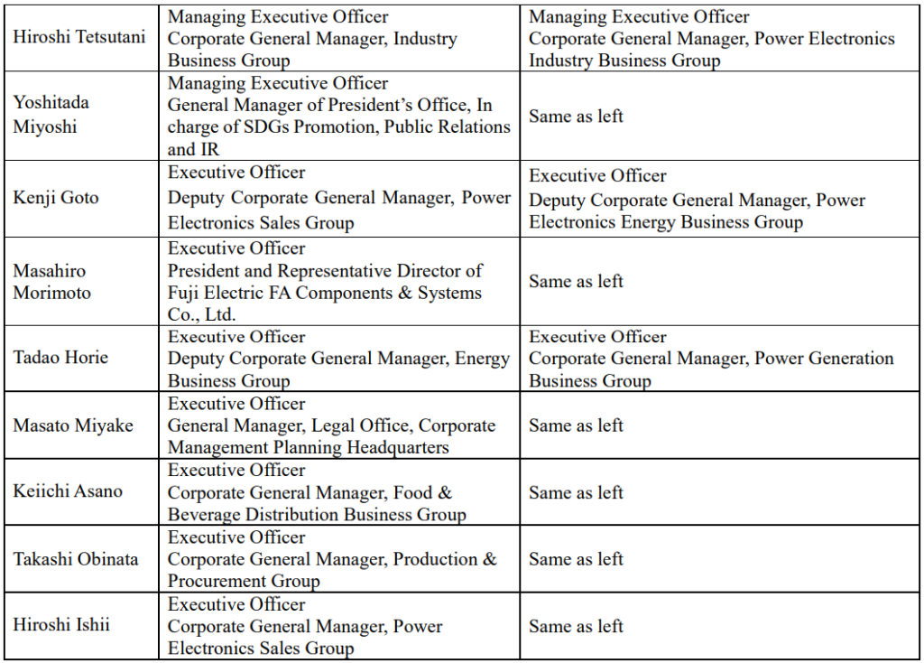
At the meeting of the Board of Directors, Fuji Electric Co., Ltd.’s organizational changes and the appointment of executive officers as of October 1 were resolved. The company will work to strengthen its proposal capabilities in the energy and environment sector by integrating the power electronics and power generation businesses.
Organizational Changes
- The Power Electronics Energy Business Group and the power generation business (thermal & geothermal, hydro, and alternative energy) of the Power Generation Business Group will be integrated to establish the new Energy Business Group.
- The Power Electronics Industry Business Group and the nuclear power business of the Power Generation Business Group will be integrated to establish the new Industry Business Group
Appointment of Executive Officers
Original – Fuji Electric
-

Littelfuse, Inc. announced the appointment of Gayla Delly to the company’s board of directors, effective September 28, 2023. Delly was also appointed to the Audit Committee.
“Gayla brings a wealth of experience as both a public company executive and seasoned board member,” said Gordon Hunter, Littelfuse Chairman of the Board of Directors. “Her board leadership and broad management experience across companies operating in a diverse set of end markets make her a terrific addition to the Littelfuse board, as we continue to execute our company’s growth strategy.
“We are pleased to welcome Gayla to the Littelfuse Board of Directors,” said Dave Heinzmann, Littelfuse Chief Executive Officer. “Gayla’s track record of driving growth and market expansion while delivering strong financial performance across industries will further strengthen our Board, as we continue our multi-year profitable growth trajectory.”
Delly retired as CEO and a member of the Board of Directors of Benchmark Electronics in 2016, where she spent 21 years in a variety of roles including President, Executive Vice President & Chief Financial Officer, Corporate Controller, and Treasurer. She began her career with KPMG. She currently serves as a director at Broadcom Inc., Flowserve Corporation, and National Instruments Corporation. Delly holds a bachelor’s degree in accounting from Samford University.
Original – Littelfuse
-
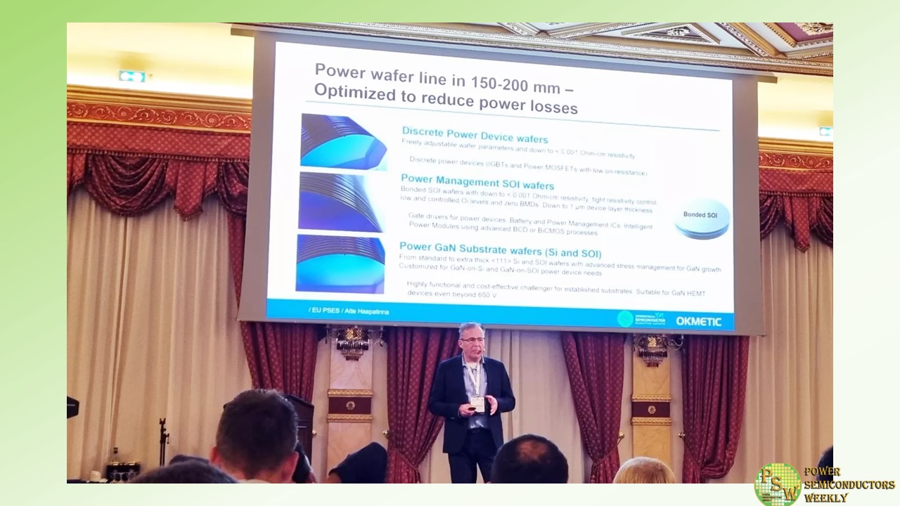
Okmetic CTO Atte Haapalinna gave a speech in September 2023 at the ISES EU Power event on Customized Silicon and SOI Wafers Enabling Enhanced Power Devices.
Advanced silicon wafers can greatly improve power device performance and reduce power losses. Okmetic Power wafer line provides an optimal platform for the manufacture of various power devices. Power device optimized wafer solutions improve power device performance, reduce Total Cost of Ownership and enable more refined designs.
Okmetic Power wafer line comprise:
- Power Management SOI wafers (Bonded SOI)
- Power GaN Substrate wafers (Si and SOI)
- Discrete Power Device wafers
Read more about Okmetic’s Power wafer line: Power Wafer Line | Okmetic
Original – Okmetic
-

GaN Systems announced the introduction of its groundbreaking 4th generation GaN power platform. This state-of-the-art technology sets a new power efficiency and compactness standard, delivering an impressive step-function performance boost and industry-leading figures of merit. For example, with GaN Systems Gen4 in an artificial intelligence (AI) server rack, 3.2kW power supplies at 100W/in3 in 2022 are now achieving 120W/in3 with efficiencies above Titanium levels. Gen4 will revolutionize power markets, including consumer electronics, data centers, solar energy, industrial applications, and automotive.
The Gen4 platform also delivers more total bill of material cost savings compared to traditional Silicon and Silicon Carbide solutions, making GaN Systems’ technology a powerful choice for businesses seeking to enhance their competitive advantage.
“Our lead customers have already realized the benefits of our Gen4 platform,” stated Jim Witham, CEO of GaN Systems. “This platform is a testament to our ongoing commitment to continuously delivering superior performance advantages and next-generation levels of efficiency. GaN Systems, in strategic collaboration with industry leaders like TSMC, has invested significantly to meet the ever-evolving demands of our customers. We are pioneering a transformation in product offerings, packaging innovations, enriched functionalities, and unparalleled performance across our markets.”
A Huge Leap for Power Electronics Technology
The Gen4 power platform boasts the following benefits:
- >20% improvement in input and output figures-of-merit translates into reduced losses, enhanced efficiency, and more cost-effective solutions.
- Increased granularity in device specification, combined with a wide range of packaging options, including PDFN, TOLL, TOLT, and Embedded – allowing the correct Rds resistance and package combination for each application, consequently optimizing electrical and thermal system performance.
- 700V E-mode with the industry’s highest transient voltage rating, 850V, significantly enhancing total system reliability and robustness. This rating enables the semiconductor components to withstand user environment anomalies, such as voltage spikes, ensuring uninterrupted and dependable performance.
- On-state resistance ranges enable power systems from 20W to 25,000W.
For more information, visit https://gansystems.com/gan-transistors/gen-4/
Original – GaN Systems
-
Researchers at the Indian Institute of Science (IISc) have developed a fully indigenous gallium nitride (GaN) power switch that can have potential applications in systems like power converters for electric vehicles and laptops, as well as in wireless communications. The entire process of building the switch – from material growth to device fabrication to packaging – was developed in-house at the Centre for Nano Science and Engineering (CeNSE), IISc.
Due to their high performance and efficiency, GaN transistors are poised to replace traditional silicon-based transistors as the building blocks in many electronic devices, such as ultrafast chargers for electric vehicles, phones and laptops, as well as space and military applications such as radar.
“It is a very promising and disruptive technology,” says Digbijoy Nath, Associate Professor at CeNSE and corresponding author of the study published in Microelectronic Engineering. “But the material and devices are heavily import-restricted … We don’t have gallium nitride wafer production capability at commercial scale in India yet.” The know-how of manufacturing these devices is also a heavily-guarded secret with few studies published on the details of the processes involved, he adds.
Power switches are used to control the flow of power to – essentially turn on or off – electronic devices. To design the GaN power switch, the IISc team used a metal organic chemical vapour deposition technique developed and optimised over a decade by researchers in the lab of Srinivasan Raghavan, Professor and Chair, CeNSE. It involves growing GaN alloy crystals layer by layer on a two-inch silicon wafer to fabricate a multi-layered transistor.
The entire process needs to be carried out carefully in a clean room to ensure that no defects arise due to environmental conditions like humidity or temperature, which can affect device performance. The team also took the help of Kaushik Basu, Associate Professor in the Department of Electrical Engineering (EE), and his lab, to build an electrical circuit using these transistors and test their switching performance.
GaN transistors typically operate in what is called a “depletion mode” – they are on all the time unless a negative voltage is applied to turn them off. But power switches used in chargers and adapters need to work the other way around – they normally need to be off and not carrying current, and should only turn on when a positive voltage is applied (“enhancement mode”). To achieve this operation, the team combined the GaN transistor with a commercially available silicon transistor to keep the device normally off.
“The packaging of the device was also indigenously developed,” explains Rijo Baby, PhD student at CeNSE and first author of the study. After packaging and testing, the team found the device performance to be comparable to state-of-the-art switches available commercially, with a switching time of about 50 nanoseconds between on and off operations.
Going forward, the researchers plan on scaling up the device dimensions so that it can operate at high currents. They also plan to design a power converter that can step up or step down voltages.
“If you look at strategic organisations in India, they have a hard time procuring GaN transistors … It is impossible to import them beyond a certain quantity or power/frequency rating,” says Nath. “This is essentially a demonstration of indigenous GaN technology development.”
Original – Indian Institute of Science (IISc)
-
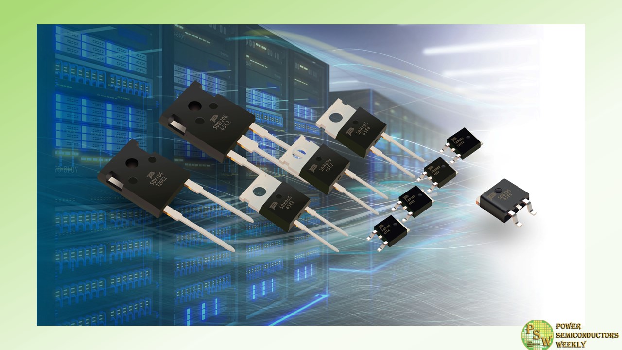
Bourns, Inc. has expanded its 650 and 1200 V Silicon Carbide (SiC) Schottky Barrier Diode (SBD) product family with 10 new models. The 10 new models added to the Bourns® SiC SBD line are designed to address the increasing power density requirements in the latest transportation, renewable energy and industrial systems.
Bourns’ expanded wide band gap diode line delivers the peak forward surge, low forward drop, reduced thermal resistance and low power loss capabilities demanded by today’s high frequency and high current applications. These capabilities also help designers develop smaller, cost-efficient and state-of-the-art power electronics.
As optimal power conversion solutions for DC-DC and AC-DC converters, Switched-Mode Power Supplies (SMPS), photovoltaic inverters, motor drives and other rectification applications, the 10 new models feature currents in the 5-10 A range, with no reverse recovery current to reduce EMI.
This enables them to significantly lower energy losses and further increase efficiency, switching performance and reliability. In addition to providing excellent thermal performance, Bourns’ new SiC SBD models are available in multiple forward voltage, current and package options that include TO220-2, TO247-3, TO252, TO263 and TO247-2.
The 10 new Bourns® BSD SiC SBD models are available now. These models are RoHS compliant, halogen free, Pb free and their epoxy potting compound is flame retardant to the UL 94V-0 standard. For more detailed product information, please see: www.bourns.com/products/diodes/silicon-carbide-sic-schottky-barrier-diodes.
Original – Bourns
-
STMicroelectronics will host its Industrial Summit 2023 at the Futian Shangri-La Hotel, in Shenzhen, China, on Sep 28.
In recognition of the extraordinary climate-related challenges, ST has long been guided by its unwavering commitment to sustainability. The Company is actively working to increase power efficiency with its cutting-edge solutions for diffused intelligence (Digitalization) and Energy and Power Conversion, forging a path towards reduced carbon emissions and a sustainable future.
The Industrial Summit is the industry’s premier technology showcase of ST’s Industrial products and solutions. The theme of this year’s event is “Powering Your Sustainable Innovation.” Visitors will hear about the Company’s focus on Smart Power and Smart Digitalization during insightful keynotes and about 30 technical sessions, while also having the chance to experience over 150 demos focused on 3 market segments: Automation, Power & Energy, and Motor Control. The Summit will also host a number of showstoppers developed in close collaboration with ST’s customers and partners.
Innovation highlights in the key focus areas
To provide ST’s Industrial customers in Asia with strong and efficient support for their development activities, ST operates three dedicated Industrial Competence Centers focused on Motor Control, Automation, and Power and Energy that are located close to customers. At Industrial Summit 2023, ST and its customers and partners will showcase multiple innovations listed below leveraging expertise and system-level solutions from these three industrial Competence Centers.
Microgrid: Microgrid is a distributed grid network that is connected to renewable sources and energy storage to minimize energy transmission loss and provide efficient energy utilization while maintaining the benefits of grid connection. ST joined forces with customers to showcase a Microgrid application with multiple energy generation and storage solutions including a photovoltaic (PV) optimizer, a string inverter, a micro-inverter, a hybrid inverter with energy storage, stand-alone energy storage, and an energy-usage example using EV charging stations.
A list of the advanced technologies ST used in this multiapplication demo includes a full range of industry-leading STM32 MCUs, breakthrough wide bandgap power technologies such as Silicon Carbide (SiC) and Gallium nitride (GaN), power metering products, and power-line communication (PLC) controllers. In particular, GaN power discretes and system-in-package devices like ST’s MasterGaN and Sti2GaN are expected to be the preferred technology for future residential PV+ energy storage system (ESS) applications that require high power density and energy efficiency.
KNX Energy Management System: KNX is a global standard with high compatibility and a huge supplier base, making it ideal for the efficient energy system in buildings. At the Industrial Summit, ST will showcase how a KNX Energy-Management System manages energy consumption and generation from various energy sources, such as Solar Inverters, Microgrid, and Battery Storage, for all aspects of applications in buildings, home appliances, and EV charging stations. The KNX Energy-Management System can play an important role in achieving carbon neutrality, enabling energy production and consumption tracking, as well as static and dynamic load management.
By adopting this system, users can proactively decide whether renewable energy should be consumed or stored, while the system provides an optimized energy solution based on user needs. STKNX is a highly competitive KNX transceiver used in a wide range of KNX products from many manufacturers. In addition, ST’s best-in-class MCU, SiC and GaN power technologies, and power conversion ICs are also utilized in this energy-management system.
Servo Drives Orchestra: According to the International Energy Agency (IEA), 53% of global electricity is consumed by motors, which makes motor-control efficiency among the most effective targets for sustainability benefits. On top of better energy performance of the motors themselves, great potential for improvement lies in how electric motors are integrated into industrial equipment and systems.
At the Summit, ST will showcase its most comprehensive motor-control demo – the Servo Drives Orchestra. This solution comprises 8 reference designs with loads ranging from 500W to 22kW. Each of the motors controls a rope that pulls a load and demonstrates high-precision position control, in harmonic movement coordinated simultaneously with the other motors. Each motor drive executes the commands sent by I/O link from the podium where an HMI (Human Machine Interface) controls the mode selection while each drive controller collects temperature and vibration data, executes condition-monitoring algorithms, and wirelessly sends data to the Baidu Cloud. The cloud then reports back system behavior and power savings, among other parameters.
ST is a leading technology provider for servo drives, power-device technologies, computational processing, isolation devices, industrial safety product, and for ecosystems, and for Industrial Automation, Predictive Maintenance, and Connectivity. The Servo Drives Orchestra demo uses an STM32 microcontroller, ST drivers, as well as SiC and GaN power solutions for overall efficiency improvement.
Efficient Transformation to Factory Automation: The use of IO-Link products in factory automation systems can simplify the installation, setup, maintenance, and repair processes, while also contributing to increased production efficiency, energy savings, and carbon neutrality. ST is committed to providing a complete solution for any IO-Link device applications, including a free IO-Link device mini stack, to help manufacturers optimize their operations and achieve greater sustainability.
ST will feature an Automated packing machine with automatic printing and labeling functions for smart factories that utilizes the Company’s IO-Link technology to manage digital input/output, sensors, and solenoid air valve drivers. The system is controlled by a PLC (Programmable Logic Controller), and the system status can be displayed and controlled on an HMI. By connecting the system to a LoRa node, the machine can be remotely monitored and controlled through the IoT Cloud via a LoRa Gateway. The machine uses Digital IO boards, sensor boards, and actuator boards developed by ST Automation Competence Center, demonstrating the comprehensive ST portfolio in action.
Original – STMicroelectronics
-

At its annual Technology Summit in Europe beginning September 27th, GlobalFoundries (GF), is highlighting key advancements to its technology platforms and solutions that will enable better power efficiency, enhanced performance and security for applications across critical end markets including IoT, smart mobile and automotive. These milestones highlight GF’s semiconductor manufacturing leadership in product development, validation and market readiness for critical applications in IoT, 5G and 6G smartphones, and electric vehicles.
Building upon the GF Technology Summit in North America this past August, the sessions in Munich will focus on leading at the edge, manufacturing semiconductors in a digital, AI-driven, world through the evolving landscape of communications infrastructure and the electrification of vehicles.
GF’s President and CEO, Dr. Thomas Caulfield, will kick-off the event with a keynote address entitled “Essential chips fuel the era of AI,” which emphasizes the transformative potential of these technologies and their significance in the rapidly evolving semiconductor landscape. In addition, Peter Schiefer, Infineon Division President Automotive, Jean-Marc Chery, President and CEO of STMicroelectronics and Karsten Schnake, Board Member for Procurement at of ŠKODA AUTO & Head of Project COMPASS at Volkswagen AG will take the stage.
Dr. Thomas Caulfield, joined by leaders in the fabless semiconductor and end-markets industries, will also share GF’s corporate vision for manufacturing the essential chips we rely on to live, work, and connect. In addition, GF’s technology and product management leaders, accompanied by partners in the semiconductor design and manufacturing ecosystem, will outline the company’s technology and solutions roadmap.
Held at the Sofitel Munich Bayerpost, the two-day summit also introduces a new format. This year, representatives from GF’s Technology, Business, and Commercial teams are on hand to host small group meetings, facilitating deeper discussions and partnerships with GF customers.
Original – GlobalFoundries
