-
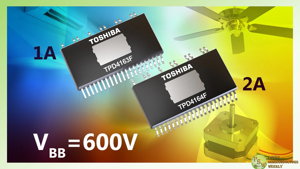
Toshiba Electronics Europe GmbH launched two products for brushless DC (BLDC) motor drive applications including fan motors, ventilation fan, air conditioners, air cleaners, and pumps.
Each of the intelligent power devices (IPD) incorporate 600V-rated IGBTs and a matched gate driver as a one-chip solution in a single compact package. The output DC current (IOUT) rating of the TPD4163F is 1A while the TPD4164F is rated at 2A.
The two devices (TPD4163F and TPD4164F) have an IGBT saturation voltage (VCEsat) of 2.6V and 3.0V respectively, while the Diode forward voltage (VF) is 2.0V and 2.5V.
Both devices are housed in a miniature surface mount HSSOP31 package. With dimensions of just 17.5mm x 11.93mm x 2.2mm, the PCB footprint is reduced by around 63% when compared with Toshiba’s existing DIP26 package products. This makes a significant contribution to reducing the space required for motor drive circuit boards.
In addition, in geographic regions where the power supply is unstable, the supply voltage may fluctuate significantly. Therefore, to improve reliability, the supply voltage rating (VBB)has been increased from 500V to 600V to introduce more design margin.
To support the new devices, Toshiba has developed a reference design for BLDC sensorless brushless DC motor drive utilizing the new TPD4164F and a microcontroller TMPM374FWUG.
Toshiba will continue to expand their product lineup with various packages and improved characteristics, contributing to customers’ design flexibility and carbon neutrality through energy-saving motor control.
Volume production shipments of both new devices (and the reference design board) start today.
Original – Toshiba
-
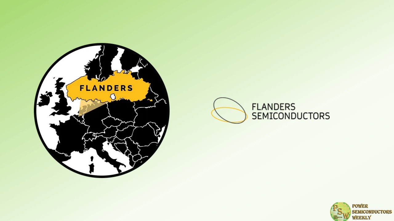
A group of semiconductor companies in Flanders have come together to create Flanders Semiconductors, a new nonprofit organization representing the interests of the industry at local, European, and global levels. The organization is open to all qualifying companies, both in and outside of the Flanders region, that have semiconductor technology at the core of their business.
Flanders Semiconductors is a significant move for the Flemish semiconductor industry, which currently employs well over 3,000 people directly, has more than 50 companies with semiconductor as their core business, and over 100 companies defining, testing, and integrating advanced customized semiconductor devices or technologies.
Flanders Semiconductors covers the whole supply chain, including infrastructure, equipment, materials, processing, testing, and devices. The Flanders region also boasts world-class research facilities such as IMEC, universities, and institutes providing semiconductor R&D, education, and training. The objectives of Flanders Semiconductors are to increase the talent pool, share industry roadmaps, maintain a yearly business events calendar, and represent members’ interests at international levels. The organization will also market the region and its members internationally, to promote cooperation between members and to cooperate with similar organizations in Europe.
Flanders Semiconductors is led by President Lou Hermans, who has over three decades of industry expertise, along with a team of seasoned semiconductor professionals. Together with the dedicated management team, their mission is to foster collaboration, drive innovation, and catalyze growth within the semiconductor ecosystem, both in Flanders and on a global scale.
“We are thrilled to officially announce the launch of Flanders Semiconductors, poised to be(come) another important European hub for semiconductor innovation,” said Lou Hermans, President of Flanders Semiconductors. “Our founding members, including BelGan, Caeleste, Cochlear, easics, ICsense, NXP, Pharrowtech, Sofics, and Spectricity, have united to create a platform that champions the semiconductor industry’s interests at every level. I am deeply inspired and motivated by the drive, support, remarkable power and unity of the founding members. Our diverse community of present and future member companies, each bringing their unique solutions to the semiconductor industry, exemplifies the immense strength and boundless potential that collaboration holds.”
Flanders Semiconductors welcomes all qualifying companies with semiconductors as their main business and is open to associate memberships for universities, R&D organizations, and non-qualifying companies.
The grand unveiling of the Flanders Semiconductor association is set for September 13th in Leuven, Belgium and interested parties can join this special occasion. Registrations to secure a spot can be done at www.flanders-semiconductors.org
Original – Flanders Semiconductors
-
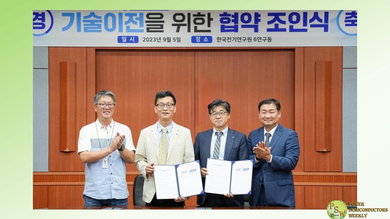
Korea Electrotechnology Research Institute (KERI) succeeded in transferring the ‘Ion Implantation and its Evaluation Technology for the SiC (silicon carbide) Power Semiconductor’ to a Hungarian company.
Power semiconductors are key components in electricity and electronics, acting as the muscles of the human body by regulating the direction of current and controlling power conversion. There are many different materials for power semiconductors. Among them, SiC is receiving the most attention due to its excellent material properties, including high durability and excellent power efficiency. When SiC power semiconductors are incorporated into electric vehicles, they cut down the power consumption of the battery and reduce the body weight and volume of the vehicle, resulting in energy efficiency improvements of up to 10%
While SiC power semiconductors have many advantages, the manufacturing process is also very challenging. Previously, a method was applied to create a device by forming an epi layer (single-crystal semiconductor thin-film) on a highly conductive wafer and flowing current through that area. However, during this process, the surface of the epi layer becomes rough and the speed of electron transfer decreases. The price of the epi wafer itself is also high, which is a major obstacle to mass production.
To solve this problem, KERI used a method of implanting ions into a semi-insulated SiC wafer without an epi layer. Ion implantation, which makes a wafer conductive, is the work that breathes life into a semiconductor.
SiC materials are hard and require very high energy ion implantation followed by high temperature heat treatment to activate the ions, making it a difficult technology to implement. However, KERI has succeeded in securing the relevant technologies based on its 10 years of experience in operating ion implantation equipment dedicated to SiC.
“Ion implantation technology can significantly reduce process costs by increasing current flow in semiconductor devices and replacing expensive epi wafers,” said Dr. Kim, Hyoung Woo, Director, Advanced Semiconductor Research Center, KERI. He continued, “This is a technology that increases the price competitiveness of high-performance SiC power semiconductors and contributes greatly to mass production.”
This technology was recently transferred to ‘SEMILAB ZRT (CEO: Tibor Pavelka)’, a semiconductor metrology equipment company located in Budapest, Hungary. With a 30-year history, SEMILAB has manufacturing plants in Hungary and the United States. SEMILAB owns patents for medium-sized precision measurement equipment and material characterization equipment, and has the world’s leading technology in semiconductor electrical parameter evaluation system.
They predict that through this technology transfer, they will be able to standardize high-quality SiC. SEMILAB plans to use KERI technology to develop specialized equipment to evaluate the ion implantation process of SiC power semiconductor.
Park Su-yong, the president of SEMILAB Korea, said, “Through the development of specialized equipment, we will be able to progress in-line monitoring of implant processes on SiC wafers for immediate, accurate, and low-cost production control of implant systems and in-line monitoring for pre-anneal implant.” He added, “This will be a great foundation for stably securing a high-quality ion implantation mass production process with excellent uniformity and reproducibility.”
KERI is a government-funded research institute under the NST (National Research Council of Science & Technology) of the Ministry of Science and ICT. It has a total of more than 120 intellectual property rights in the field of power semiconductor research. As of the last 10 years, power semiconductor division of KERI has achieved more than KRW 3 billion in technology transfers, the highest level in South Korea.
Original – KERI
