-

Vishay Intertechnology, Inc. announced that it has been honored by DENSO Corporation, a leading mobility supplier, with a 2022 Collaboration Award.
The 2022 Collaboration Awards recognize suppliers that have continued to provide DENSO with key components that keep production lines moving for the company and its customers, despite the tight supply market. Previously this year, Vishay was also recognized by DENSO with a 2022 North America Business Partner of the Year Award in the Quality Leader category.
“Vishay has demonstrated a strong commitment to supporting DENSO on both a working and management level,” said Kouji Arima, CEO of DENSO. “We sincerely appreciate the company’s unsparing efforts and contributions, and know we can count on them regardless of the market situation. We look forward to building an even stronger partnership with Vishay as we continue working together.”
“We are deeply honored to receive this acknowledgment from DENSO of our unwavering support during challenging market conditions,” said Joel Smejkal, President and CEO at Vishay. “This recognition underscores our commitment to operational excellence and the strength of our partnership with the company. We look forward to building on this level of collaboration to grow together in the coming years.”
Original – Vishay Intertechnology
-

Texas Instruments announced its new 300-mm semiconductor wafer fabrication plant in Richardson, Texas, RFAB2, achieved LEED (Leadership in Energy and Environmental Design) Gold certification under version 4 (v4). This designation makes RFAB2 the first wafer fab in the United States and the fourth in the world to achieve this more stringent certification from the U.S. Green Building Council (USGBC) for the sustainable design, construction and operation of high-performance green buildings.
“One of TI’s ambitions is to be a company that our employees are personally proud to be a part of and would want as our neighbor,” said Brian Dunlap, vice president, 300-mm Wafer Fab Manufacturing Operations at Texas Instruments. “We are proud that RFAB2 has achieved LEED Gold v4 certification, underscoring TI’s long-standing commitment to operate in a socially thoughtful and environmentally responsible manner.”
RFAB2, which is TI’s fourth LEED-certified manufacturing plant, was designed to reduce water and electricity usage. In fact, the new fab’s design, construction and operation are expected to achieve significant efficiencies, including saving 750 million gallons of potable water and almost 80,000 megawatt-hours of energy annually. The factory was also constructed using responsibly sourced materials and was designed and built in a way that fosters a healthy work environment.
“What makes this LEED Gold designation impressive is that Texas Instruments achieved this high standard developed for office buildings in a semiconductor manufacturing plant,” said Jill Kurtz, director of Building Sciences at Page, who consulted TI in the certification process. “By prioritizing sustainability and transparency, TI is delivering real impact in water and energy savings, leading the way in their industry and helping USGBC continue toward its goal of green buildings for everyone within this generation.”
The LEED Gold v4 certification solidifies TI’s dedication to responsible, sustainable manufacturing, including multi-year goals and programs focused on conserving natural resources, reducing energy consumption and mitigating environmental impact. To learn more about TI’s commitment to sustainability, download the company’s latest Corporate Citizenship Report.
Original – Texas Instruments
-
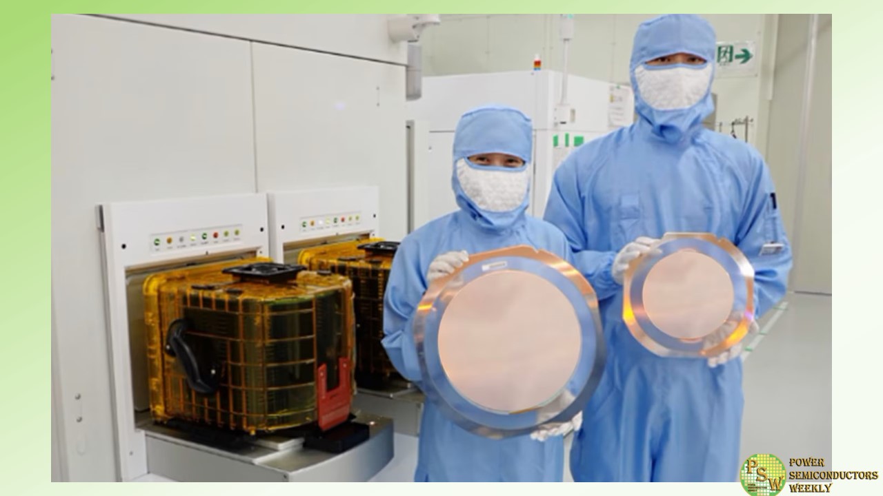
Mitsubishi Electric Corporation has completed installation of its first 12-inch silicon wafer processing line at its Power Device Work’s Fukuyama Factory, which manufactures power semiconductors. In addition, through sample production and testing, it has been verified that the power semiconductor chips processed on this production line achieve the required performance levels.
As previously announced, Mitsubishi Electric is planning to start mass production on the new 12-inch silicon wafer line in fiscal 2025. The company aims to approximately double its silicon power semiconductor wafer processing capacity by fiscal 2026 compared to fiscal 2021 levels.
In recent years, the demand for power semiconductors offering efficient control of electrical power is growing as countries look to achieve carbon-free status. Power semiconductors are utilized in wide range of relevant products, including electric vehicles, consumer devices (e.g. air-conditioning systems), industrial equipment, renewable energy and traction devices, and a stable supply is required in order to meet this growing demand.
Mitsubishi Electric will contribute to the realization of a carbon-free society through enhancement of its production capacity and by ensuring a stable supply of power semiconductors through the introduction of highly efficient 12-inch wafer production lines.
Original – Mitsubishi Electric
-
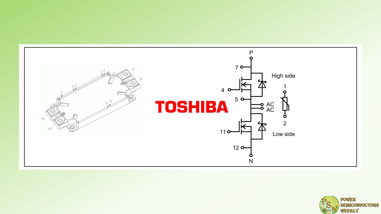
Toshiba Electronic Devices & Storage Corporation developed “MG250YD2YMS3,” the industry’s first 2200V dual silicon carbide (SiC) MOSFET module for industrial equipment. The new module has a drain current (DC) rating of 250A and uses the company’s third generation SiC MOSFET chips. It is suitable for applications that use DC1500V, such as photovoltaic power systems and energy storage systems. Volume shipments start today.
Industrial applications like those mentioned above generally use DC1000V or lower power, and their power devices are mostly 1200V or 1700V products. However, anticipating widespread use of DC1500V in coming years, Toshiba has released the industry’s first 2200V product.
MG250YD2YMS3 offers low conduction loss with a low drain-source on-voltage (sense) of 0.7V (typ.). It also offers lower turn-on and turn-off switching loss of 14mJ (typ.) and 11mJ (typ.) respectively, an approximately 90% reduction against a typical silicon (Si) IGBT. These characteristics contribute to higher equipment efficiency. Realizing low switching loss also allows the conventional three-level circuit to be replaced with a two-level circuit with a lower module count, contributing to equipment miniaturization.
Toshiba will continue to meet the market needs for high efficiency and the downsizing of industrial equipment.
Applications
Industrial Equipment
- Renewable energy power generation systems (photovoltaic power systems, etc.)
- Energy storage systems
- Motor control equipment for industrial equipment
- High frequency DC-DC converter, etc.
Features
- Low drain-source on-voltage (sense):
VDS(on)sense=0.7V (typ.) (ID=250A, VGS=+20V, Tch=25°C) - Low turn-on switching loss:
Eon=14mJ (typ.) (VDD=1100V, ID=250A, Tch=150°C) - Low turn-off switching loss:
Eoff=11mJ (typ.) (VDD=1100V, ID=250A, Tch=150°C) - Low stray inductance:
LsPN=12nH (typ.)
Original – Toshiba
-
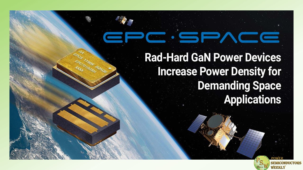
EPC Space announced the introduction of two new rad-hard GaN transistors with ultra-low on-resistance and high current capability for high power density solutions that are lower cost and more efficient than the nearest comparable radiation-hardened silicon MOSFET. These devices come packaged in hermetic packages in very small footprints.
The EPC7020G is a 200 V, 14.5 mΩ, 200 Apulsed radiation-hardened gallium nitride transistor and the EPC7030G is a 300 V, 32 mΩ, 200 Apulsed radiation-hardened gallium nitride transistor. These devices join the 40 V, 4.5 mΩ EPC7019G and the 100 V, 4.5 mΩ EPC7018G to cover applications including power supplies for satellites and space mission equipment, motor drives for robotics, instrumentation and reaction wheels, and deep space probes. This product family comes packaged in a compact hermetic package in a footprint less than 45 mm2.
Part Number Drain to Source Voltage (VDS) Drain to Source Resistance (RDS(on)) Single-Pulse Drain Current (IDM) EPC7019G 40 V 4 mΩ 530 A EPC7018G 100 V 6 mΩ 345 A EPC7020G 200 V 14.5 mΩ 200 A EPC7030G 300 V 32 mΩ 200 A With higher breakdown strength, lower gate charge, lower switching losses, better thermal conductivity, and lower on-resistance, power devices based on GaN significantly outperform silicon-based devices and enable higher switching frequencies resulting in higher power densities, higher efficiencies, and more compact and lighter weight circuitry for critical spaceborne missions.
“The G-Package family offers the lowest on-resistance of any packaged rad hard transistor currently on the market,” said Bel Lazar, CEO of EPC Space. “These devices offer mission-critical components with superior figure of merit, significantly smaller size, and lower cost for the space and other high-reliability markets than alternative rad hard silicon solutions”.
Original – EPC Space
