-
GaN / LATEST NEWS / TOP STORIES / WBG2 Min Read
Shin-Etsu Chemical Co., Ltd. has announced a major development milestone for its QST™ substrate—a 300-mm GaN growth substrate—achieved through collaboration with IMEC.
The 300-mm QST™ substrate was adopted in IMEC’s recently launched 300-mm GaN power device development program. In initial evaluations, a 5 µm-thick HEMT (High Electron Mobility Transistor) structure fabricated on Shin-Etsu’s QST™ substrate demonstrated a record-breaking voltage resistance exceeding 800 V. This represents the highest breakdown voltage ever achieved on a 300-mm GaN substrate that complies with SEMI standards and confirms the substrate’s outstanding in-plane uniformity and crystal quality.
The QST™ substrate was developed by QROMIS, Inc., based in California, and licensed to Shin-Etsu Chemical. Shin-Etsu manufactures 150-mm, 200-mm, and 300-mm QST™ substrates, as well as GaN-on-QST™ epitaxial wafers. In September 2024, the company began offering 300-mm QST™ sample substrates in collaboration with QROMIS, strengthening its commitment to advancing large-diameter GaN manufacturing.
This partnership has enabled Shin-Etsu to supply QST™ substrates for IMEC’s CMOS-based 300-mm GaN fab. The joint program aims to develop both 650 V-rated and future 1200 V+ GaN power devices targeted for high-performance applications, including AI data centers, automotive systems, and industrial power electronics.
The QST™ substrate’s thermal expansion coefficient is closely matched to GaN, which facilitates stable crystal growth and reduces challenges such as wafer warpage that typically hinder high-yield GaN growth on silicon at larger diameters. By solving these limitations, the QST™ platform allows for the cost-effective production of thick-film GaN devices on 300-mm wafers—a key factor in scaling next-generation power semiconductors.
Manufacturing was carried out using Aixtron’s Hyperion MOCVD equipment, which enabled the precise deposition of the HEMT structure during testing. The results confirmed superior yield potential and mechanical integrity at the 300-mm scale, marking a crucial step toward practical large-scale manufacturing of GaN power devices.
Shin-Etsu is currently preparing for mass production of 300-mm QST™ substrates and has already enhanced its facilities for 150-mm and 200-mm variants. The QST™ substrate lineup, ranging from 150 mm to 300 mm, is being evaluated by domestic and international partners for applications in power conversion, RF, and LED markets, particularly in light of growing demand for high-efficiency systems in data centers and electric vehicles.
With its scalable GaN technology, Shin-Etsu aims to accelerate the adoption of GaN devices and support the shift toward more sustainable and energy-efficient technologies across the global electronics industry.
Original – Shin-Etsu Chemical
-
GaN / LATEST NEWS / PRODUCT & TECHNOLOGY / TOP STORIES / WBG2 Min Read
Shin-Etsu Chemical Co., Ltd. has created a 300-mm (12-inch) QSTTM substrate, which is a substrate dedicated to GaN epitaxial growth, and recently started supplying samples.
Shin-Etsu Chemical has sold 150-mm (6-inch) and 200-mm (8-inch) QSTTM substrates and GaN on QSTTM epitaxial substrates of each diameter. Meanwhile, the company worked on further increasing the diameter in response to strong customer demand and successfully developed a 300-mm (12-inch) QSTTM substrate. GaN device manufacturers cannot benefit from increasing the diameter of materials because of the lack in large-diameter substrate suitable for GaN growth, despite the fact that they can use the existing Si production line for GaN.
This 300-mm QSTTM substrate enables GaN epitaxial growth without warping or cracks, which was unattainable on Si substrates, thus significantly reducing device costs. In addition to the enhancement of facilities for 150-mm and 200-mm QSTTM substrates already in progress, Shin-Etsu Chemical will work on mass-producing 300-mm QSTTM substrates.
Since QSTTM substrates have the same coefficient of thermal expansion as that of GaN, it is possible to constrain warping and cracks of GaN epitaxial layer on QSTTM substrate of the SEMI standard thickness. This substrate material allows for high-quality and thick GaN epitaxial growth with a large diameter. Leveraging this feature, many customers are evaluating QSTTM substrates and GaN on QSTTM epitaxial substrates for power devices, high-frequency devices, and LEDs. Despite the challenging business environment, customers have entered the development phase toward practical to address the recently increasing interest in power devices, including power supplies for data centers.
The addition of the 300-mm QSTTM substrate to the lineup of the 150-mm and 200-mm can significantly accelerate the spread of GaN devices. Shin-Etsu Chemical is committed to contribute to the realization of a sustainable society where energy can be used efficiently through the social implementation of GaN devices.
Original – Shin-Etsu Chemical
-
GaN / LATEST NEWS / PRODUCT & TECHNOLOGY / TOP STORIES / WBG3 Min Read
Qromis, Inc. brings a revolutionary, high performance substrate solution for large-diameter GaN epi and device wafers. Rather than solving incremental scale and performance challenges of conventional substrates for WBG semiconductors, QST™ (Qromis Substrate Technology) has been developed and validated as a disruptive solution, with cross-functional optimization.
In this approach, the key properties of substrate material such as stress, lattice mismatch, thermal stability and shape control are engineered independently for the best fit with GaN epitaxial and device layers, as well as with different device architectures and performance targets. QST™ materials layers are integrated together in the conventional semiconductor fab with a simple manufacturing flow.
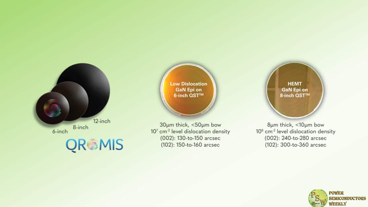
The resulting large diameter substrates (6-inch, 8-inch, 12-inch or beyond) are capable of supporting from a few to tens of microns of high-quality GaN epitaxy, from which unique, high performance and low cost GaN device structures are fabricated.Qromis is designing reference devices for device manufacturers to demonstrate the benefits of the groundbreaking QST™ technology. These devices exploit key advantages of QST™ over other substrate solutions:
– High quality and stress-free GaN,
– Ability to deposit thick, bulk-like GaN epi layers on large diameter substrates,
– Low defectivity, eliminating a major limitation to performance and scalability.
With these distinct features, designers can now break free from the current technological limitations of GaN process technologies and develop advanced device architectures for lateral and vertical device designs of light emitters, switches, rectifiers, as well as monolithic and integrated circuits.Qromis, Inc., established in March 2015 and located in Silicon Valley, California, is a privately held fabless technology innovator focusing on energy efficient and high performance wide bandgap (WBG) semiconductor materials and device solutions which dramatically reduce global energy use and consumption. The Company is poised to become one of the premier players in the rapidly growing, multi-billion dollar WBG industry with its disruptive and validated solutions in substrate and device technologies, which enable an unmatched cost, performance, and application scale. Markets served include power electronics, light emitting diodes (LEDs), advanced displays, and RF electronics, and other emerging high performance and energy efficient applications.
As a fabless company, Qromis is driving the commercialization of its unique solutions in conjunction with its foundry network. The Company and its foundry partner offer WBG device foundry services, as well as access to advanced and novel process technology platforms, for its customers and partners.To learn more about Qromis and its substrate technology, join the International Conference on Compound Semiconductor Manufacturing Technology which takes place May 20-23, 2024 in Tucson, Arizona.
Original – Qromis