-

At this month’s IEEE Energy Conversion Congress and Expo (ECCE), Navitas Semiconductor introduced conference attendees to ‘IntelliWeave’ – an innovative patented new digital control technique for improving next generation AI data center power supply (PSU) efficiency.
In a world where ever-more energy is needed for the processing of artificial intelligence (AI) and cloud-based applications, minimizing power consumption has become a priority for data center architects and operators. Combining next-generation GaN and SiC semiconductors with new control technique strategies to power conversion plays a key role in achieving this goal.
IntelliWeave’s novel digital control enables highest system efficiencies with precision current sharing, ultra-fast dynamic response and minimal phase error. A patented dual-loop and dual-feed-forward interleaving control achieves absolute zero voltage switching (ZVS) across the full-load range to enable highest efficiencies.
The digital control for Critical Conduction Mode (CRM) interleaving Totem Pole Power Factor Control (PFC) enables 30% reduction in power losses compared to existing Continuous Conduction Mode (CCM) solutions. The digital control combined with high-power GaNSafe power ICs has been proven on a 500 kHz GaN-based interleaving 3.2 kW CrM PFC PSU operating at 99.3% peak efficiency including EMI filter loss.
Taking place in Phoenix, Arizona from October 20th to 24th, IEEE ECCE 2024 features both industry-driven and application-oriented technical sessions and brings together practicing engineers, researchers and other professionals for interactive and multidisciplinary discussions on the latest advances in various areas related to energy conversion.
On October 21st Tao Wei presented “Novel digital control for a GaN-based CrM interleaved TP PFC”.
Original – Navitas Semiconductor
-

Navitas Semiconductor announced GaNSlim™, a new generation of highly-integrated GaN power ICs that will further simplify and speed the development of small form factor, high-power-density applications by offering the highest level of integration and thermal performance.
GaNSlim enables the simplest, fastest, and smallest system design by integrating drive, control, and protection, with integrated EMI control and loss-less current sensing, all within a high thermal performance proprietary DPAK-4L package. Additionally, with an ultra-low startup current below 10 µA, GaNSlim devices are compatible with industry-standard SOT23-6 controllers and eliminate HV startup.
Integrated features such as loss-less current sensing eliminate external current sensing resistors and optimize system efficiency and reliability. Over-temperature protection ensures system robustness and auto sleep-mode increases light and no-load efficiency. Autonomous turn-on/off slew rate control maximizes efficiency and power density while reducing external component count, system cost and EMI.
GaNSlim features a patented, 4-pin, high-thermal-performance, low-profile, low-inductance, DPAK package. This package enables 7 °C lower temperature operation versus conventional alternatives, supporting high-power-density designs with ratings up to 500 W. Target applications include chargers for mobile devices and laptops, TV power supplies, lighting, etc.
“Our GaN focus is on integrated devices that enable high-efficiency, high-performance power conversion with the simplest designs and the shortest possible time-to-market,” says Reyn Zhan, Sr. Manager of Technical Marketing. “Our new GaNSlim portfolio – built on integration, ease-of-use, and low-cost manufacturing methods, – continues to grow the customer pipeline with over 50 new projects already identified. GaNSlim increases our GaN addressable market by enabling lower system costs compared to silicon designs for many applications, targeting applications under 500 W across mobile, consumer and home appliance.”
Devices in the NV614x GaNSlim family are rated at 700 V with RDS(ON) ratings from 120 mΩ to 330 mΩ and are available in versions optimized for both isolated and non-isolated topologies.
As with other Navitas GaN ICs, GaNSlim devices are supplied with an industry-leading twenty-year warranty, while demo boards for QR flyback, single-stage PFC, boost PFC plus QR flyback and TV power supply designs allow for rapid evaluation and selection of the optimum device for a given application.
Original – Navitas Semiconductor
-

Navitas Semiconductor announced that its high-power GaNSafe family is now available in a TOLT (Transistor Outline Leaded Top-side cooling) package.
The GaNSafe family has been specifically created to serve demanding, high-power applications, such as AI data centers, solar/energy storage, and industrial markets. Navitas 4th generation integrates control, drive, sensing, and critical protection features that enable unprecedented reliability and robustness. GaNSafe is the world’s safest GaN with short-circuit protection (350ns max latency), 2kV ESD protection on all pins, elimination of negative gate drive, and programmable slew rate control. All these features are controlled with 4-pins, allowing the package to be treated like a discrete GaN FET, requiring no VCC pin.
The TOLT packaging enhances thermal dissipation through the top side of the package, allowing heat to be dissipated directly to the heatsink (not through the PCBA). This enables the reduction of operating temperature and increases current capability, resulting in the highest level of system power density, efficiency, and reliability.
“With over 200 million units shipped and supplied with a 20-year warranty, Navitas’ highly integrated high-power GaNSafe ICs are proven to deliver performance and reliability while simplifying Design-IN for systems up to 22kW,” says Charles Bailley, Senior Director of Business Development. “As the most protected, reliable, and safe GaN devices in the industry, GaNSafe took our technology into mainstream applications above 1kW. Now, with the enhanced thermal dissipation of the TOLT package, we are enabling customers to deliver even better performance, efficiency, power density, and reliability in even the most demanding applications.”
Suitable for applications from 1 kW to 22 kW, 650 V GaNSafe in TOLT packaging is available with a range of RDS(ON)MAX from 25 to 98 mΩ. Integrated features and functions include:
- High-speed short-circuit protection, with autonomous ‘detect and protect’ with ultra-fast 350 ns / 50 ns latency.
- Protected, regulated, integrated gate-drive control, with zero gate-source loop inductance for reliable high-speed 2 MHz switching capability to maximize application power density.
- Electrostatic discharge (ESD) protection of 2 kV, compared to zero for discrete GaN transistors.
- 650 V continuous, and 800 V transient voltage capability for extraordinary application conditions.
- Integrated Miller Clamp (no negative gate bias, higher 3rd quadrant efficiency)
- Programmable turn-on and turn-off speeds (dV/dt) to simplify EMI regulatory requirements.
- Simple 4-pin device, allowing the package to be treated like a discrete GaN and requiring no additional VCC pin
- Robust, thermally enhanced packaging: ultra-low RQ_JUNC-AMB and board-level thermal cycling (BLTC) Reliability
In addition to the new ICs, Navitas will be offering reference design platforms based on GaNSafe TOLT for applications including data center power supplies and EV on-board chargers. These system platforms include complete design collateral with fully tested hardware, embedded software, schematics, bill-of-materials, layout, simulation, and hardware test results.
Original – Navitas Semiconductor
-

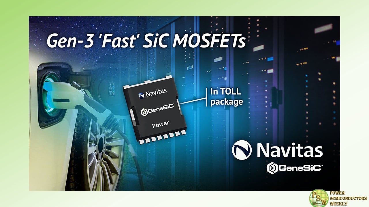
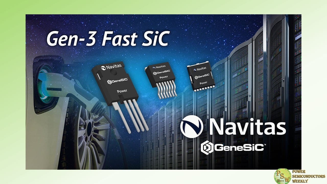
Navitas Semiconductor announced the release of a portfolio of third-generation automotive-qualified SiC MOSFETs in D2PAK-7L (TO-263-7) and TOLL (TO-Leadless) surface-mount (SMT) packages.
Navitas’ proprietary ‘trench-assisted planar’ technology provides world-leading performance over temperature and delivers high-speed, cool-running operation for electric vehicle (EV) charging, traction, and DC-DC conversion. With case temperatures up to 25°C lower than conventional devices, Gen-3 Fast SiC offers an operating life up to 3x longer than alternative SiC products, for high-stress EV environments.
Gen-3 Fast MOSFETs are optimized for the fastest switching speed, highest efficiency, and support increased power density in EV applications such as AC compressors, cabin heaters, DC-DC converters, and on-board chargers (OBCs). Navitas’ dedicated EV Design Center has demonstrated leading edge OBC system solutions up to 22 kW with 3.5 kW/liter power density, and over 95.5% efficiency.
400 V-rated EV battery architectures are served by the new 650 V Gen-3 Fast MOSFETs featuring RDS(ON) ratings from 20 to 55 mΩ. The 1,200 V ranges from 18 to 135 mΩ and is optimized for 800 V systems.
Both 650 and 1,200 V ranges are AEC Q101-qualified in the traditional SMT D2PAK-7L (TO-263-7) package. For 400 V EVs, the 650 V-rated, surface-mount TOLL package offers a 9% reduction in junction-to-case thermal resistance (RTH,J-C), 30% smaller PCB footprint, 50% lower height, and 60% smaller size than the D2PAK-7L. This enables very high-power density solutions, while minimal package inductance of only 2 nH ensures excellent fast-switching performance and lowest dynamic package losses.
The automotive-qualified 650 V and 1200 V G3F SiC MOSFET family in D2PAK-7L and TOLL surface mount packages are released and available immediately for purchase.
Original – Navitas Semiconductor
-
Navitas Semiconductor announced unaudited financial results for the second quarter ended June 30, 2024.
“We are pleased with our Q2 results at the high end of our guidance, major new design wins, and significant technology advances and launches,” said Gene Sheridan, CEO and co-founder. “Our leading- edge technology is fueling robust customer pipeline growth in each end market, led by AI data centers with multiple customers ramping production with our GaN and SiC-based power systems.”
2Q24 Financial Highlights
- Revenue: Total revenue grew to $20.5 million in the second quarter of 2024, a 13% increase from $18.1 million in the second quarter of 2023.
- Loss from Operations: GAAP loss from operations for the quarter was $31.1 million, compared to a loss of $27.2 million for the second quarter of 2023. On a non-GAAP basis, loss from operations for the quarter was $13.3 million compared to a loss of $9.6 million for the second quarter of 2023.
- Cash: Cash and cash equivalents were $112.0 million as of June 30, 2024, with no debt.
Market, Customer and Technology Highlights
- Enterprise / AI Data Center: Growing family of AC-DC power platforms up to 10 kW to meet nVidia’s Hopper-Blackwell-Rubin roadmap, with up to 480 kW power demand per rack. Optimized combination of industry-leading Gen-3 Fast SiC and GaNSafe™ technologies sets new AC-DC efficiency (97%) and power density (140 W/in3) benchmarks. Customer pipeline doubled since December ’23 investor day, with over 60 customer projects in development, and another 7 data center design wins in Q2.
- EV / eMobility: Strong growth in customer pipeline, now with over 200 projects. Strong interest in 22 kW on-board charger platform, contributing to 15 design wins in Q2, and on-track for first GaN revenues in EV by the end of 2025.
- Appliance / Industrial: Customer pipeline grew beyond the $380 million stated in December, with revenue ramp expected in 2025 across diverse customers and regions, including 7 of the top 10 appliance leaders. 25 new project wins expected to ramp production in 2025 or 2026, including haircare, washers, dryers, refrigerators, heat pumps, industrial HVAC, robotics and automation applications.
- Solar / Energy Storage: As displacement technologies, SiC (for string inverters and storage) and GaN (for micro-inverters) are replacing legacy silicon chips, with over 100 customer projects, including the majority of the top 10 solar players. 6 new commercial design wins in Q2, and on track for expected US GaN-based micro-inverter ramp next year.
- Mobile / Consumer: Mobile customers increasing GaN adoption for their fast-charger portfolios. GaN adoption at Xiaomi and OPPO is expected to be 30% in 2024. Following wins for Samsung’s Galaxy S23 and S24 phones, Navitas now powers chargers for Samsung’s new Galaxy Z Flip6, Z Fold6 and all A-series phones. In notebook PCs, GaNFast was adopted again by Lenovo and Dell. Overall, another 16 GaNFast chargers launched in Q2, bringing the all-time total to over 470 designs, and Navitas remains #1 in mobile fast charging.
- New GaNSlim™ Portfolio: with integration, ease-of-use and low-cost manufacturing methods – continues to grow the customer pipeline, now with over 50 customer projects across mobile, consumer and home appliance markets.
Business Outlook
Third quarter 2024 net revenues are expected to be $22.0 million plus or minus $500 thousand. Non-GAAP gross margin for the third quarter is expected to be 40% plus or minus 50 basis points and non-GAAP operating expenses are expected to be approximately $21.5 million.
Original – Navitas Semiconductor
-

Navitas Semiconductor announced that Samsung had expanded adoption of Navitas’ GaNFast ICs from the original flagship Galaxy S22, S23 and S24 to the mainstream Galaxy A, and revolutionary Galaxy Z Fold6 and Galaxy Z Flip6 smartphones with enhanced Galaxy AI features.
GaN runs up to 20x faster than legacy silicon and enables chargers up to 3x more power and 3x faster charging in half size and weight. GaNFast power ICs enable high-frequency, high-efficiency power conversion, achieving up to a 50% shrink vs. prior designs.
The new 25W charger (EP-T2510) features new energy-saving technology to reduce standby losses by 75% to only 5 mW, which aligns with Navitas’ environmental advances, where every GaNFast IC saves 4 kg of CO2 vs. legacy silicon chips.
“Since enabling the world’s first production GaN charger in 2018, Navitas has pioneered and leads the adoption of GaN to replace legacy silicon chips,” noted David Carroll, Sr. VP Worldwide Sales for Navitas. “Our production partnership with Samsung dates back to the Galaxy S22 Ultra, and today’s announcement reflects the dramatic expansion of GaN from niche, flagship designs to adoption in high-volume, mainstream phones.”
Original – Navitas Semiconductor
-
Navitas Semiconductor extended its new portfolio of Gen-3 ‘Fast’ (G3F) 650 V SiC MOSFETs into a thermally-enhanced, rugged, high-speed, surface-mount TOLL (Transistor Outline Leadless) package designed for demanding, high-power, high-reliability applications.
Combining high-power capability and best-in-class low on-resistance of 20 to 55 mΩ, these 650 V SiC MOSFETs have been optimized for the fastest switching speed, highest efficiency, and increased power density demanded by applications such as AI data center power supplies, EV charging and energy storage and solar solutions (ESS).
Navitas’ GeneSiC products use a proprietary ‘trench-assisted planar’ technology that provides world-leading efficiency performance over the temperature range, with G3F MOSFETs delivering high-speed, cool-running performance that ensures up to 25°C lower case temperatures and up to 3x longer life than alternative SiC products.
Navitas’ latest 4.5 kW AI power system reference design features the G3F45MT60L (650V 40 mΩ, TOLL) G3F SiC MOSFET in an interleaved CCM-TP PFC topology. Complemented by the NV6515 (650V, 35mΩ, TOLL) GaNSafe™ Power IC in the LLC stage, the 4.5 kW solution has a peak efficiency above 97% and, at 137 W/inch3, it is the world’s highest power density AI PSU. For 400 V-rated EV battery systems, G3F in TOLL is an ideal technology for on-board chargers (OBC), DC-DC converters, and traction drives ranging from 6.6 to 22 kW.
The surface-mount TOLL package offers a 9% reduction in junction-to-case thermal resistance (RTH,J-C), 30% smaller PCB footprint, 50% lower height, and 60% smaller size than the traditional D2PAK-7L, enabling highest-power-density solutions, as demonstrated in the 4.5 kW AI solution. Additionally, with a minimal package inductance of only 2 nH, excellent fast-switching performance and lowest dynamic losses are achieved.
The G3F family in TOLL package is released and available for purchase.
Original – Navitas Semiconductor
-
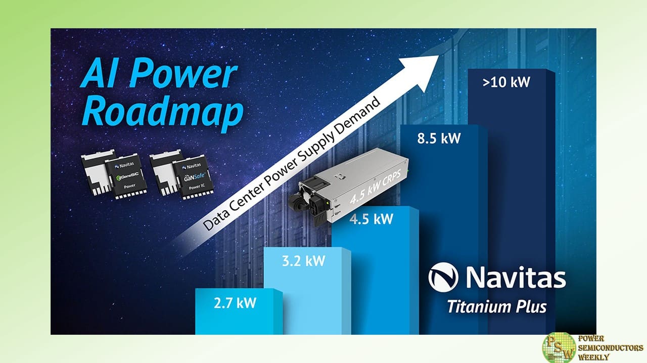
Navitas Semiconductor released its 4.5 kW AI data center power supply reference design, with optimized GaNSafe™ and Gen-3 ‘Fast’ (G3F) SiC power components. The optimized design enables the world’s highest power density with 137 W/in3 and over 97% efficiency.
Next-generation AI GPUs like NVIDIA’s Blackwell B100 and B200 each demand over 1 kW of power for high-power computation, 3x higher than traditional CPUs. These new demands are driving power-per-rack specifications from 30-40 kW up to 100 kW.
Navitas announced its AI Power Roadmap in March 2024, showcasing next-generation data center power solutions for the growing demand in AI and high-performance computing (HPC) systems. The first design was a GaNFast-based 3.2 kW AC-DC converter in the Common Redundant Power Supply (CRPS) form factor, as defined by the hyperscale Open Compute Project. The 3.2 kW CRPS185 (for 185 mm length) enabled a 40% size reduction vs. the equivalent legacy silicon approach and easily exceeded the ‘Titanium Plus’ efficiency benchmark, critical for data center operating models and a requirement for European data center regulations.
Now, the latest 4.5 kW CRPS185 design demonstrates how new GaNSafe™ power ICs and GeneSiC Gen-3 ‘Fast’ (G3F) MOSFETs enables the world’s highest power density and efficiency solution. At the heart of the design is an interleaved CCM totem-pole PFC using SiC with full-bridge LLC topology with GaN, where the fundamental strengths of each semiconductor technology are exploited for the highest frequency, coolest operation, optimized reliability and robustness, and highest power density and efficiency. The 650 V G3F SiC MOSFETs feature ‘trench-assisted planar’ technology which delivers world-leading performance over temperature for the highest system efficiency and reliability in real-world applications.
For the LLC stage, 650 V GaNSafe power ICs are ideal and unique in the industry with integrated power, protection, control, and drive in an easy-to-use, robust, thermally-adept TOLL power package. Additionally, GaNSafe power ICs offer extremely low switching losses, with a transient-voltage capability up to 800 V, and other high-speed advantages such as low gate charge (Qg), output capacitance (COSS), and no reverse-recovery loss (Qrr). High-speed switching reduces the size, weight, and cost of passive components in a power supply, such as transformers, capacitors, and EMI filters. As power density increases, next-gen GaN and SiC enable sustainability benefits, specifically CO2 reductions due to system efficiency increases and ‘dematerialization’.
The 3.2 kW and 4.5 kW platforms have already generated significant market interest with over 30 data center customer projects in development expected to drive millions in GaN and SiC revenue, ramping from 2024 into 2025.
Navitas’ AI data center power supply reference designs dramatically accelerate customer developments, minimize time-to-market, and set new industry benchmarks in energy efficiency, power density and system cost, enabled by GaNFast power ICs and GeneSiC MOSFETs. These system platforms include complete design collateral with fully tested hardware, embedded software, schematics, bills-of-material, layout, simulation, and hardware test results.
“AI is dramatically accelerating power requirements of data centers, processors and anywhere AI is going in the decades to come creating a significant challenge for our industry. Our system design center has stepped up to this challenge delivering a 3x increase in power in less than 18 months”, said Gene Sheridan, CEO of Navitas Semiconductor. “Our latest GaNFast technology, combined with our G3F SiC technology are delivering the highest power density and efficiency the world has ever seen…the perfect solution for the Blackwell AI processors and beyond.”
Original – Navitas Semiconductor
-
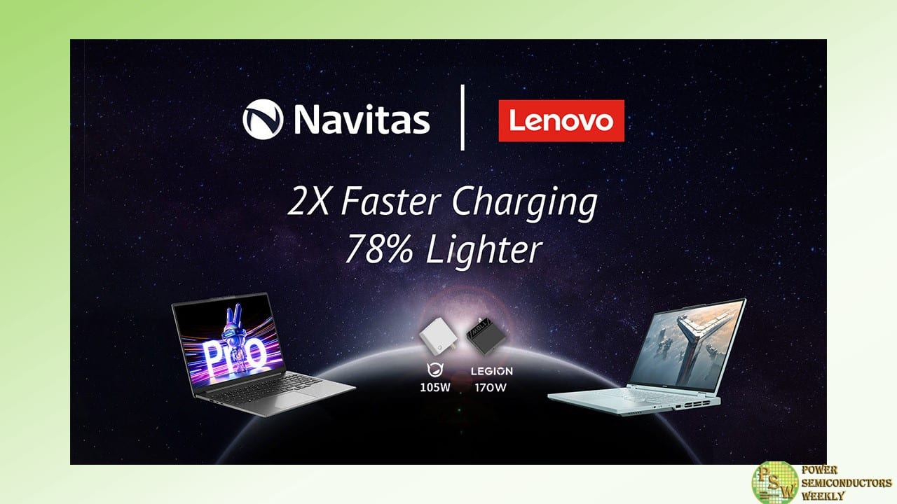
Navitas Semiconductor announced that its GaNFast power ICs have been selected to lead Lenovo’s latest GaN technology chargers; Xiaoxin 105 W GaN charger, and the Legion C 170 W GaN charger, respectively designed for daily travel and gaming power, bringing consumers a brand new fast charging experience.
The Xiaoxin 105 W GaN charger is designed for daily travel. It outputs 105 W of power and is equipped with 3 ports (2C1A) supporting multiple protocols; easily achieving the charging needs of various devices simultaneously. At only 206 g, the 105 W fast-charger is 41% lighter than a typical 100 W computer adapter and takes only 34 minutes to charge the Xiaoxin 16 Pro to 50%. The Navitas NV6138 GaNFast power IC with GaNSense™ technology is at the heart of the high-frequency flyback topology design, providing a stable, durable, and efficient charging experience.
The Legion C170 W GaN charger is designed specifically for hardcore gamers. It delivers 170 W of continuous power through a single port to meet the high-power demands of gaming devices. At only 245 grams, it’s 78% lighter than Legion Y9000P’s original inbox charger and can charge up to 2 times faster than the Legion C140 W Charger. The Navitas NV6136 GaNFast power IC with GaNSense technology is used in the PFC stage, featuring loss-less current sensing and 6 times faster short-circuit protection than competing solutions, delivering cooler operation, superior efficiency, reliability, and power density.
Lenovo’s long-term collaboration with Navitas has brought a series of groundbreaking fast chargers to the market and played a significant role in raising market awareness on showcasing the benefits of GaN technology. At the Lenovo YOGA CC65 dual-port GaN charger launch event in 2021, Navitas’ 6-inch GaN wafer and GaNFast power ICs were publicly showcased for the first time, unveiling the mysteries of this leading technology to consumers.
In terms of gaming products, Navitas collaborated with Lenovo to create a 90 W charger for the Lenovo Legion Pro Gaming Phone and a 135 W, C135 W GaN charger for the Legion 5 and 5 Pro Gen 7 laptops. For lightweight travel, Lenovo developed a series of compact, lightweight powerful GaN chargers using Navitas technology, including the revolutionary compact Thinkplus ‘lipstick’ and the ultra-thin Thinkbook ‘biscuit’ charger.
Lenovo and Navitas are not only partners in power technology but also pioneers in sustainability. Lenovo Group is verified by the Science Based Targets initiative (SBTi) for net zero targets and Navitas is the world’s first power semiconductor company to achieve CarbonNeutral® certification. Navitas’ advanced GaN technology enables Lenovo to continuously create smaller, lighter chargers with higher power density, significantly reducing the number of passive and magnetic components inside the charger, achieving CO2 reduction in production through “dematerialization”. The increased efficiency reduces power loss during use, thus further lowering carbon emissions in the product lifecycle.
“With the support of Navitas GaNFast power ICs, we have successfully introduced two new Xiaoxin and Legion GaN chargers to the market, enabling a lightweight and powerful charging experience for daily travel and gaming performance,” said Elon Chen, Product Manager of Consumer Business for Lenovo Group China. “Moreover, the successful application of Navitas’ GaNFast technology continuously reduces the size and weight of chargers, highly increasing efficiency, bringing convenience to consumers, while contributing to carbon reduction.”
“Powerland is very pleased to collaborate with Navitas again to create two high-performance and lightweight GaN chargers for Lenovo,” said Dr. Wang Chuanyun, VP of R&D for Powerland Group. “Powerland is dedicated to pushing the envelope of technology to build leading power products for our clients. Efficient, reliable, and easy-to-use GaNFast power ICs are crucial to realize that.”
“Navitas is very honored to enter Lenovo’s supply chain twice in a short period, providing high-efficiency and stable GaNFast fast charging power into two important Lenovo products,” said Charles Zha, VP and GM of Navitas China. “By working closely with Powerland, our highly integrated GaNFast technology has enabled Lenovo to continuously achieve leading-edge results in size, performance, and reliability of chargers. With innovative laptops like AI PCs on the rise, Navitas predicts a surge in demand for powerful GaNFast charging solutions. Navitas is on a mission to push the limits of gallium nitride technology, empowering global partners like Lenovo to slash energy usage and emissions in charger and adapter production. Together, we will speed towards a greener, more sustainable planet!”
Original – Navitas Semiconductor
-
Navitas Semiconductor announced their new portfolio of Gen-3 ‘Fast’ (G3F) 650 V and 1,200 V SiC MOSFETs optimized for fastest switching speed, highest efficiency, and increased power density for applications such as AI data center power supplies, on-board chargers (OBCs), fast EV roadside super-chargers, and solar / energy-storage systems (ESS). The broad portfolio range covers industry-standard packages from D2PAK-7 to TO-247-4, designed for demanding, high-power, high-reliability applications.
The G3F family is optimized for high-speed switching performance, resulting in 40% improvement to hard-switching figures-of-merits (FOMs) compared to competition in CCM TPPFC systems. This will enable increasing the wattage of next-generation AI power supply units (PSUs) up to 10 kW, and power per rack increase from 30 kW to 100-120 kW.
The G3F GeneSiC MOSFETs are developed using a proprietary ‘trench-assisted planar’ technology. and offer better-than-trench MOSFET performance, while also providing superior robustness, manufacturability and cost than competition. G3F MOSFETs deliver high-efficiency with high-speed performance, enabling up to 25°C lower case temperature, and up to 3x longer life than SiC products from other vendors.
The ‘trench-assisted planar’ technology enables an extremely low RDS(ON) increase versus temperature, which results in the lowest power losses across the complete operating range and offers up to 20% lower RDS(ON) under real-life operation at high temperatures compared to competition.
Additionally, all GeneSiC MOSFETs have the highest-published 100%-tested avalanche capability, 30% longer short-circuit withstand time, and tight threshold voltage distributions for easy paralleling, GeneSiC MOSFETs are ideal for high-power, fast-time-to-market applications.
Navitas’ latest 4.5 kW high-power density AI Server PSU reference design in CRPS185 form-factor, showcases the 650 V-rated, 40mOhms G3F FETs for an Interleaved CCM TP PFC topology. Alongside the GaNSafe™ Power ICs in the LLC stage, a power density of 138 W/inch3 and peak efficiency above 97% is realized, which comfortably achieves ‘Titanium Plus’ efficiency standards, now mandatory in Europe.
For the EV market, 1,200 V/34 mOhm (G3F34MT12K) G3F FETs enable Navitas’ new 22 kW, 800V Bi-Directional OBC and 3KW DC-DC converter to achieve a superior power density of 3,5 kW/L and a peak efficiency of 95.5%.
“G3F sets a new standard for efficient, cool-running SiC performance, coupled with high reliability and robustness for high-power, high-stress systems,” noted Dr. Sid Sundaresan, Senior Vice President of SiC Technology and Operations. “We’re pushing the boundaries of SiC, with up to 600 kHz switching speeds, and hard-switching figures-of-merit up to 40% better than competition.”
Original – Navitas Semiconductor
